

)
)
F
XC9128/XC9129 Series
ETR0411-010a
1A Driver Transistor Built-In, Step-Up DC/DC Converters
■GENERAL DESCRIPTION
The XC9128/XC9129 series are synchronous step-up DC/DC converters with a 0.2 (TYP.) N-channel driver transistor and a
synchronous 0.2 (TYP.) P-channel switching transistor built-in. A highly efficient and stable current can be supplied up to
1.0A by reducing ON resistance of the built-in transistors. With a high switching frequency of 1.2MHz, a small inductor is
selectable making the series ideally suited for applications requiring low profile or space saving solutions. With the MODE
pin, the series provides mode selection of PWM control or PFM/PWM automatic switching control. In the PWM/PFM
automatic switching mode, the series switches from PWM to PFM to reduce switching loss when load current is small.
When load current is large, the series switches automatically to the PWM mode so that high efficiency is achievable over a
wide range of load conditions. The series also provides small output ripple from light to large loads by using the built-in
circuit which enables the smooth transition between PWM and PFM. With a adaptor enable function of the XC9128 series,
when a voltage higher than the input voltage is applied to the output, the input and the output become isolated making it
possible for the IC to work in parallel with the likes of an AC adaptor.
■APPLICATIONS
●Digital audio equipment
●Digital cameras, Video equipment
●Computer Mouses
●Various multi-function power supplies using alkali cells (1
to 3 cells), nickel hydride batteries, or single lithium cells
■ FEATURES
High Efficiency, Large Current Step-Up Converter
Output Current : 150mA@V
Input Voltage Range : 0.8V~6.0V
Output Voltage Setting
Range
Oscillation Frequency : 1.2MHz (Fixed oscillation frequency
Input Current : 1.0A
Maximum Current Limit : 1.2A (MIN.), 2.0A (MAX.)
Control : PWM, PWM/PFM control
High Speed
Transient Response
Protection Circuits : Thermal shutdown
Soft-Start Time : 5ms (TYP.) internally set
Ceramic Capacitor Compatible
Adaptor Enable Function (XC9128 series)
Flag Output (XC9128 series) : Open-drain output
Operating Ambient Temperature
Packages : MSOP-10, USP-10B
Environmentally Friendly
☆GreenOperation Compatible
=3.3V, VIN=0.9V
=1.8V, I
OUT
=3.3V, VIN=1.8V
OUT
=3.3V,
OUT
=10mA→100mA
OUT
500mA@V
: 1.8V~5.3V (Externally set)
Set up freely with a reference voltage
supply of 0.45V (±0.010V) & external
components
accuracy ±15%)
externally selectable
:100mV @ V
V
IN
Integral latch method (Over current
limit)
: - 40℃~+85℃
: EU RoHS Compliant, Pb Free
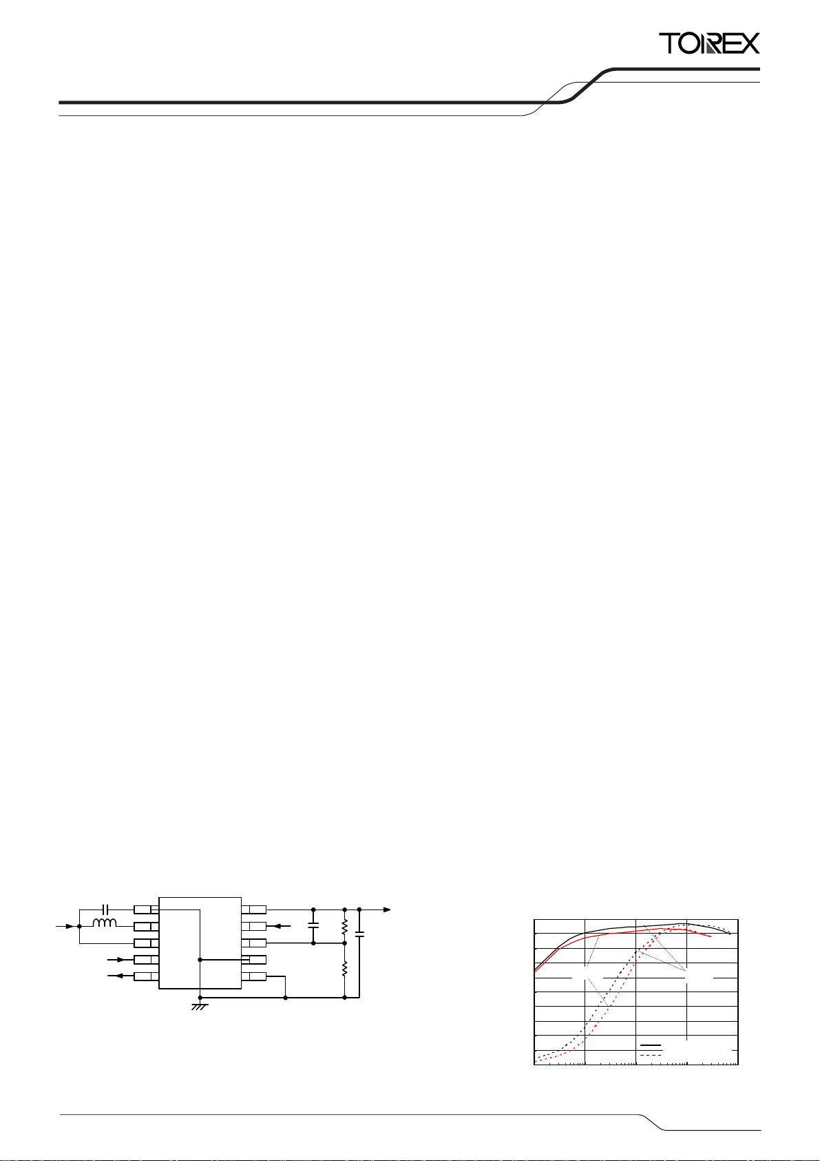
■TYPICAL APPLICATION CIRCUIT
V
C
IN
IN
L
EN
FO
PGND
1
2
Lx
BAT
3
EN
4
FO
5
VOUT
MODE
AGND
AEN/
10
MODE
C
9
FB
8
7
6
R
FB1
FB
R
FB2
V
C
L
(ceramic)
OUT
■TYPICAL PERFORMANCE
CHARACTERISTICS
●Efficiency vs. Output Current
XC9128B45CD
L=4.7μH(LTF5022-LC),CL=30μF(LMK212BJ106KG ×3
100
90
80
70
60
50
40
30
Efficiency: EFFI (%
20
10
0
0.1 1 10 100 1000
1.8V
Output Current: I
V
=3.3V,VEN=6V,VFO=OPEN,V
OUT
R
=270kΩ,R
FB1
OUT
=43kΩ,CFB=12pF,CIN=10μ
FB2
3.0V
PW M/PFM (V
PWM (V
MODE=VOUT
(mA)
MODE
=0V)
)
=0V
AEN/
1/26
XC9128/XC9129 Series
■PIN CONFIGURATION
P
1
GND
Lx 2
BAT 3
EN 4
FO 5
MSOP-10
(TOP VIEW)
■PIN ASSIGNMENT
10 V
OUT
9 MODE
8 FB
7 A
GND
6 AEN/
FO 5
EN 4
BAT 3
P
GND
NC 5
EN 4
BAT 3
P
GND
Lx 2
1
USP-10B
(BOTTOM VIEW)
XC9128 Series
Lx 2
1
USP-10B
(BOTTOM VIEW)
XC9129 Series
6 AEN/
7 A
GND
8 FB
9 MODE
10 V
OUT
6 NC
7 A
GND
8 FB
9 MODE
10 V
OUT
PIN NUMBER
MSOP-10*
USP-10B*
(XC9128)
USP-10B*
(XC9129)
PIN NAME FUNCTION
1 1 1 PGND Power Ground
2 2 2 Lx Output of Internal Power Switch
3 3 3 BAT Battery Input
4 4 4 EN Chip Enable
5 5 - FO Flag Output
6 6 - AEN/ Adaptor Enable
7 7 7 AGND Analog Ground
8 8 8 FB Output Voltage Monitor
9 9 9 MODE Mode Switch
10 10 10 VOUT Output Voltage
- - 5, 6 NC No Connection
*For MSOP-10 and USP-10B packages, please short the GND pins (pins 1 and 7).
*The dissipation pad for the USP-10B package should be solder-plated following the recommended mount pattern and metal masking
so as to enhance mounting strength and heat release. If the pad needs to be connected to other pins, it should be connected to the
Ground pins (pins 1 and 7).
2/26
■FUNCTION CHART
1. EN, AEN/ Pin Function
●XC9128 Series
EN PIN AEN/ PIN
L→H L
H H→L Lower than 0.45×0.8V Operation Available
H H→L Higher than 0.45×0.95V Operation Not Available
H H -
L L
L H
* Do not leave the EN and AEN/ Pins open.
●XC9129 Series
EN PIN IC OPERATIONAL STATE
H Operation
L Disable
* Do not leave the EN Pin open.
2. MODE Pin Function
●XC9128/XC9129 Series
MODE PIN FUNCTION
H PWM Control
L PWM/PFM Automatic Switching Control
FB PIN VOLTAGE
-
-
-
XC9128/XC9129
Series
IC OPERATIONAL STATE SOFT-START FUNCTION
Operation Available
Step-Up Operation
Shut-Down
Disable Disable -
-
3/26
XC9128/XC9129 Series
■PRODUCT CLASSIFICATION
●Ordering Information
XC9128①②③④⑤⑥-⑦
DESIGNATOR ITEM SYMBOL DESCRIPTION
① Integral Protection
②③ Reference Voltage 45
④ Oscillation Frequency C 1.2MHz
(*1)
⑤⑥-⑦
XC9129①②③④⑤⑥-⑦
DESIGNATOR ITEM SYMBOL DESCRIPTION
① Integral Protection
②③ Reference Voltage 45
④ Oscillation Frequency C 1.2MHz
⑤⑥-⑦
(*1)
The “-G” suffix denotes Halogen and Antimony free as well as being fully RoHS compliant.
(*1)
4/26
(*1)
・・・・Adaptor Chip Enable Pin and Flag Output Pin are added
B With integral protection
D Without integral protection
Fixed reference voltage 0.45V
②=4, ③=5
AR MSOP-10 (1,000/Reel)
Packages
(Order Unit)
AR-G MSOP-10 (1,000/Reel)
DR USP-10B (3,000/Reel)
DR-G USP-10B (3,000/Reel)
(*1)
・・・・Adaptor Chip Enable Pin and Flag Output Pin are not added
B
With integral protection
(under development)
D Without integral protection
Fixed reference voltage 0.45V
②=4, ③=5
Package
(Order Unit)
DR USP-10B (3,000/Reel)
DR-G USP-10B (3,000/Reel)
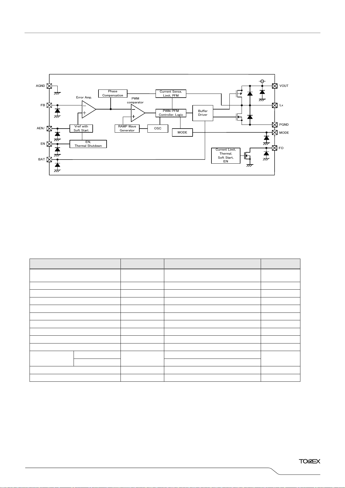
■BLOCK DIAGRAM
●XC9128 Series
* XC9129 Series
The XC9129 series does not have AEN/ pin and FO pin.
■ABSOLUTE MAXIMUM RATINGS
PAR AMETER SYMBOL RATINGS UNITS
V
Pin Voltage VOUT - 0.3~6.5 V
OUT
AEN/ Pin Voltage
FO Pin Voltage
FO Pin Current
FB Pin Voltage VFB - 0.3~6.5 V
BAT Pin Voltage VBAT - 0.3~6.5 V
MODE Pin Voltage VMODE - 0.3~6.5 V
EN Pin Voltage VEN - 0.3~6.5 V
LX Pin Voltage VLx - 0.3~V
LX Pin Current ILx 2000 mA
Power Dissipation
Operating Ambient Temperature Topr - 40~+85
Storage Temperature Tstg - 55~+125
AGND, PGND is the standard voltage for all of voltages.
*1: When implemented on a PCB.
The XC9129 series does not have AEN/ pin and FO pin. These pins are available only in the XC9128 series.
*2:
(*2)
VAEN/ - 0.3~6.5 V
(*2)
VFO - 0.3~6.5 V
(*2)
IFO 10 mA
+0.3 V
OUT
150
(*1)
MSOP-10 350
USP-10B
Pd
XC9128/XC9129
Series
Ta =2 5℃
mW
o
C
o
C
5/26
XC9128/XC9129 Series
■ELECTRICAL CHARACTERISTICS
XC9128/XC9129 Series
LX SW "Nch" ON Resistance RLxN VIN=V
Integral Latch Time (XC9128)
Integral Latch Time (XC9129)
PAR AMETER SYMBOL CONDITIONS MIN. TYP. MAX.
Input Voltage VIN - - - 6.0 V -
FB Voltage VFB
Output Voltage Setting Range VOUTSET - 1.8 - 5.3 V ①
Operation Start Voltage VST1
Oscillation Start Voltage VST2
Operation Hold Voltage VHLD
Supply Current 1 IDD1 VIN = V
Supply Current 2 (XC9128) - 30 80
IDD2
Supply Current 2 (XC9129)
Input Pin Current I
Stand-by Current I
Oscillation Frequency f
Maximum Duty Cycle
Minimum Duty Cycle
BAT
STB
OSC
MAXDTY
MINDTY
PFM Switching Current IPFM
Efficiency
(*2)
EFFI
LX SW "Pch" ON Resistance RLxP
LX Leak Current ILXL VIN=V
Current Limit
(*5)
ILIM V
(*6)
(*6)
tLAT
Soft-Start Time 1 tSS1
Soft-Start Time 2
Soft-Start Time 3
Thermal Shutdown
Temperature
(*7)
tSS2
(*7)
tSS3
T
TSD - - 150 -
Hysteresis Width THYS - - 20 -
Output Voltage Drop
Protection
(*6)
FO Output Current
FO Leakage Current
(*7)
IFO_OUT
(*7)
IFO_Leak VIN = V
V
LVP
×0.9
(*3)
(*8)
(*8)
(*8)
(*8)
(*4)
VEN=0V
,
,
,
V
OUT=VIN
=3.3V, VFO=0V
Voltage to start oscillation during
= 0.46V → 0.44V
V
FB
Connect to external components,
RL=1kΩ
Connect to external components,
RL=33Ω
Voltage to start oscillation during
VIN=0V → 1V, RL=1kΩ
Connect to external components, RL=1kΩ
=3.3V, VFB=0.45V×0.9 - 3 6 mA ②
OUT
VIN = V
OUT
=3.3V
VFB=0.45V×1.1 (Oscillation stop),
V
=0V
MODE
V
V
=3.3V, V
IN
= V
IN
= V
V
IN
VIN = V
VIN = V
=1.8V, VEN=0V - 2 10 μA ③
OUT
=3.3V, VEN=0V - 2 10 μA ②
OUT
=3.3V, VFO=0V
OUT
VFB=0.45V
=3.3V, VFO=0V
OUT
V
=0.45V×0.9
FB
=3.3V, VFO=0V
OUT
VFB=0.45V×1.1
Connect to external components,
V
=0V, RL=330Ω
MODE
Connect to external components,
=33Ω
R
L
VIN=VLx=V
+50mV,
OUT
VFB=0.45V×1.1
=3.3V, Lx =50mV
OUT
= VLX, VFB=0V - 1 - μA ⑤
OUT
>2.5V 1.2 1.5 2.0 A ①
OUT
Time to stop oscillation during
=33Ω → 3.3Ω, VFO=L → H
R
L
Time to stop oscillation during
=33Ω → 3.3Ω
R
L
Time to start oscillation during
→ V
at VIN = V
IN
=3.3V, VFO=0V,
OUT
VFB=0.45V×0.95
VIN = V
=3.3V, VFO=0V,
OUT
VFB=0.45V×0.95
Time to start oscillation during
V
AEN/=VIN
= V
V
IN
OUT
V
→0V.
=3.3V, VFO=0V,
=0.45V×0.8
FB
Time to start oscillation during
V
AEN/=VIN
→0V
VIN =3.3V
Voltage to stop oscillation during
=1.56V→1.3V
V
OUT
VIN =V
=3.3V, VFO=0.25V 1.3 1.7 2.2 mA ④
OUT
=3.3V, VEN=0V ,VFO=1V - 0 1 μA ④
OUT
0.44 0.45 0.46 V ④
- - 0.8 V ①
- - 0.9
- 0.8 - V ①
- 0.7 - V ①
- 28 78
1.02 1.20 1.38 MHz ④
85 92 96 % ④
- - 0 % ④
- 250 400 mA ①
- 93 - % ①
- 0.20
-
0.20
- 3.5 - ms ①
1.7 5.3 10.5 ms ④
- 0.02 0.04 ms ④
1.7 5.3 10.5 ms ④
1.3 1.48 1.56 V ⑥
0.35
(*1)
0.35
Topr=25 oC
UNITS CIRCUIT
(*1)
V ①
μA ②
(*1)
Ω ⑤
(*1)
Ω ⑦
o
C -
o
C -
6/26

)
)
XC9128/XC9129
Series
■ELECTRICAL CHARACTERISTICS (Continued
UNITS
AEN/
=0V
Topr=25oC
CIRCUIT
(*8)
●XC9128/XC9129 Series (Continued
PAR AMETER SYMBOL CONDITIONS MIN. TYP. MAX.
EN "H" Voltage VENH
EN "L" Voltage VENL
MODE "H" Voltage VMODEH RL =330Ω, Voltage operates at PWM control 0.65 - 6.0 V
MODE "L" Voltage VMODEL RL =330Ω, Voltage operates at PFM control AGND - 0.2 V
AEN/ Voltage
EN "H" Current IENH
EN "L" Current IENL
MODE "H" Current IMODEH
MODE "L" Current IMODEL
AEN/ "H" Current
AEN/ "L" Current
FB "H" Current IFBH
FB "L" Current IFBL
Test Conditions:
For the Circuit No.3, unless otherwise stated,
For the Circuit No.7, unless otherwise stated, V
External Components:
*
1 : Designed value
*
2 : Efficiency ={(output voltage) X (output current)} ÷ {(input voltage) X (input current)} X 100
*
3 : LX SW "P-ch" ON resistance=(VLx-V
*
4 : Testing method of LX SW "N-ch" ON resistance is stated at test circuits.
*
5 : Current flowing through the Nch driver transistor is limited.
*
6 : The XC9128D/XC9129D series does not have integral latch protection and V
This is only available with the XC9128B/XC9129B series.
*
7 : The XC9129 series does not have FO and AEN/ pins. These pins are only available in the XC9128 series.
*
8 : The XC9129 series does not have FO and AEN/ pins. The AEN/FO functions are only effective for the test of the XC9128 series.
(*7)
VAEN/
(*7)
IAEN/H
(*7)
IAEN/L
For the Circuit No.1, unless otherwise stated, V
For the Circuit No.2, unless otherwise stated, V
For the Circuit No.4, unless otherwise stated,
For the Circuit No.5, unless otherwise stated,
For the Circuit No.6, unless otherwise stated,
For the Circuit No.1, R
C
For the Circuit No.2,3, C
For the Circuit No.4,6, C
For the Circuit No.5, C
For the Circuit No.7, C
=10μF(ceramic), CIN=10μF(ceramic)
L2
VIN =V
Voltage to start oscillation during
VFB=0.45V×0.9, VEN= 0.2V→0.65V
VIN = V
Voltage to stop oscillation during
VIN = V
Voltage to start oscillation during V
V
V
IN=VOUT=VFB
VIN=V
VIN=V
VIN=V
VIN=V
VIN=V
=270kΩ, R
FB1
=1μF(ceramic)
IN
=1μF(ceramic), Rpull=300Ω
IN
=1μF(ceramic), C
IN
=1μF(ceramic), C
IN
pin test voltage)÷100mA
OUT
=3.3V, VFO=0V
OUT
=3.3V, VFO=0V
OUT
VFB=0.45V×0.9,
V
= 0.65V→0.20V
EN
=3.3V, VFO=0V
OUT
IN=VOUT=VFB=VEN
=6.0V, VEN=0V -0.1 - - μA
OUT=VFB=VMODE
OUT=VFB
OUT
VIN=V
=6.0V, V
OUT=VFB=VAEN/
=6.0V, VEN=0V, V
OUT=VFB
=6.0V, VFB=0V -0.1 - - μA
OUT
=43kΩ, CFB=12pF, L=4.7μH(LTF5022 TDK), CL1=22μF(ceramic),
FB2
=6.0V - - 0.1 μA
OUT
OUT
(*8)
0.65 - 6.0 V ④
(*8)
- - 0.2 V ④
= 0.9V→0.7V
AEN/
0.7 0.8 0.9 V ④
=6.0V - - 0.1 μA
=6.0V - - 0.1 μA
=0V -0.1 - - μA
MODE
=6.0V - - 0.1 μA
=0V -0.1 - - μA
AEN/
=1.8V, VEN=V
IN
=1.8V, VFB =0V, VEN=V
IN
VIN=1.8V, V
VIN=1.8V, VFB=0V, VEN=V
VIN=3.3V, V
VEN=V
MODE
EN=VMODE
MODE=VFO
OUT=VEN=VMODE
=0V
AEN/
=Vpull=VFO=3.3V, VFB=0V
=3.3V
=3.3V, V
MODE
=3.3V, FB=0V
MODE
(*8)
=3.3V, V
=Vpull=VFO=3.3V, V
=1μF(ceramic)
=1μF(ceramic), SBD =XBS304S17(TOREX), Rpull=0.5Ω
function.
LVP
AEN/
=0V
AEN/
(*8)
(*8)
=0V
(*8)
7/26
①
①
②
②
②
②
②
②
②
②
XC9128/XC9129 Series
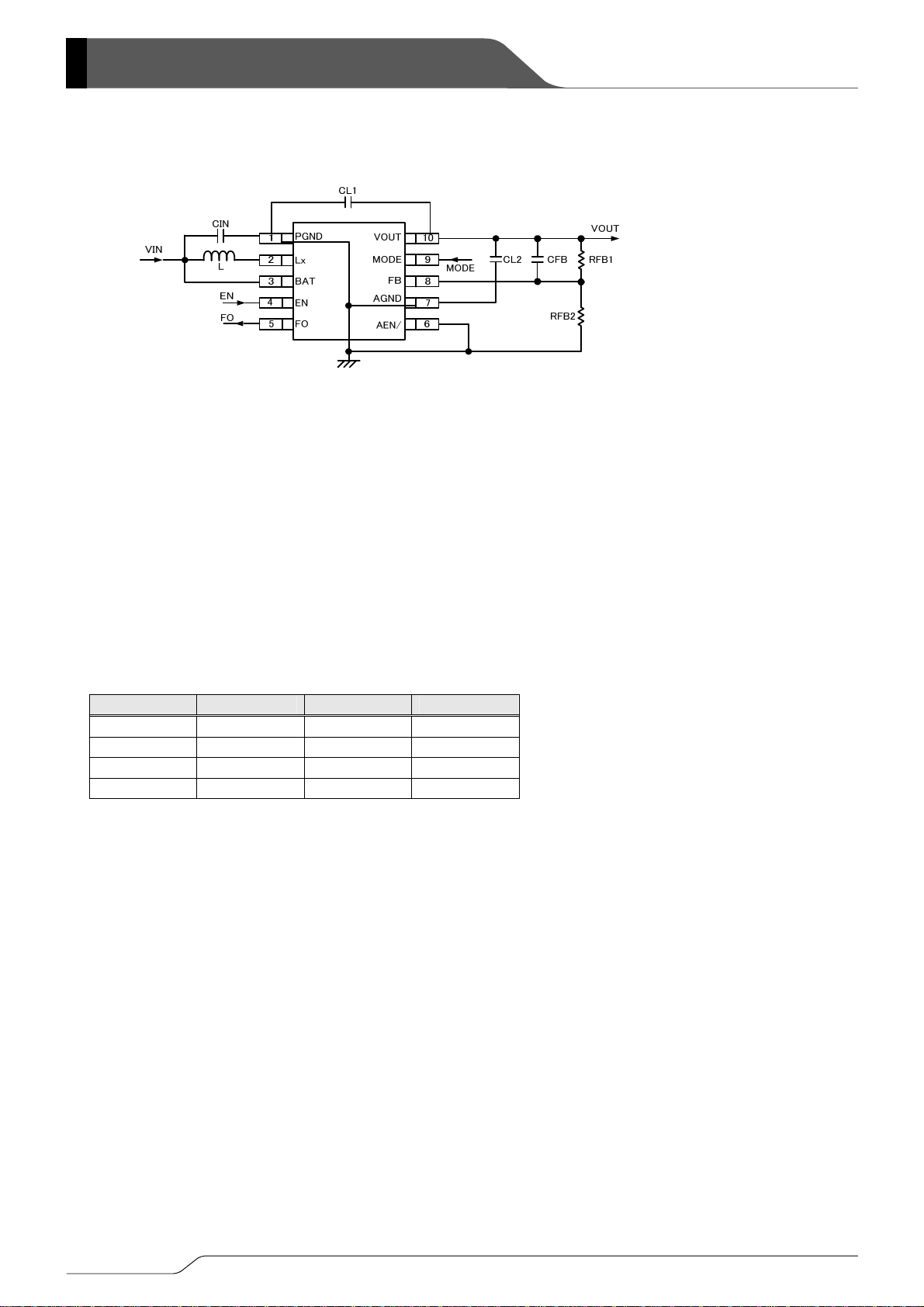
■TYPICAL APPLICATION CIRCUIT
<Output Voltage Setting>
Output voltage can be set by adding external split resistors. Output voltage is determined by the following equation,
based on the values of R
OUT=0.45 × (RFB1 + RFB2) / RFB2
V
The value of C
the range of 10 kHz to 60 kHz. Adjustments are depending on application, inductance (L), load capacitance (CL) and
dropout voltage.
[Example of calculation]
When R
VOUT1 = 0.45 × (270k+43k ) / 43k = 3.276V
[Typical example]
FB1=270kΩ, RFB2=43kΩ,
VOUT (V)
1.8 300 100 10
2.5 270 59 12
3.3 270 43 12
5.0 180 17.8 15
[External Components]
1.2MHz:
L : 4.7μH (LTF5022-4R7-LC TDK)
: 4.7μH (CDRH4D28C-4R7N SUMIDA)
CL1 : 22μF (ceramic)
CL2 : 10μF (ceramic)
CIN : 10μF (ceramic)
* C
should be selected in 10μF or higher.
L1
Capacitance C
If C
L1
In case of the usage C
check actual performance on the board.
* If using Tantalum or Electrolytic capacitors please be aware that ripple voltage will be higher due to the larger
ESR (Equivalent Series Resistance) values of those types of capacitors. Please also note that the IC’s
operation may become unstable with such capacitors so we recommend that you fully check actual
performance.
, speed-up capacitor for phase compensation, should be f
FB
is lower than 10μF, operation may be unstable.
8/26
FB1 and RFB2. The sum of RFB1 and RFB2 should normally be 500k or less.
= 1 / (2 x
ZFB
RFB1 (kΩ) RFB2 (kΩ)
+ CL2 is recommended 30μF or higher. (Ceramic capacitor compatible)
L1
L1
+ C
<30μF, output ripple may increase so that we recommend that you fully
L2
CFB (pF)
x
CFB1 x RFB1) which is in

XC9128/XC9129
Series
■OPERATIONAL EXPLANATION
The XC9128/XC9129 series consists of a reference voltage source, ramp wave circuit, error amplifier, PWM comparator,
phase compensation circuit, N-channel driver transistor, P-channel synchronous rectification switching transistor and current
limiter circuit. The error amplifier compares the internal reference voltage with the FB pin feed back voltage via resistors
FB1 and RFB2. Phase compensation is performed on the resulting error amplifier output, to input a signal to the PWM
R
comparator to determine the turn-on time of the N-channel driver transistor during PWM operation. The PWM comparator
compares, in terms of voltage level, the signal from the error amplifier with the ramp wave from the ramp wave circuit, and
delivers the resulting output to the buffer driver circuit to cause the Lx pin to output a switching duty cycle. This process is
continuously performed to ensure stable output voltage. The current feedback circuit monitors the N-channel driver
transistor’s turn-on current for each switching operation, and modulates the error amplifier output signal to provide multiple
feedback signals. This enables a stable feedback loop even when a low ESR capacitor, such as a ceramic capacitor, is
used, ensuring stable output voltage.
<Reference Voltage Source>
The source provides the reference voltage to ensure stable output of the DC/DC converter.
<Ramp Wave Circuit>
The ramp wave circuit determines switching frequency. The frequency is fixed internally at 1.2MHz. The Clock generated
is used to produce ramp waveforms needed for PWM operation, and to synchronize all the internal circuits.
<Error Amplifier>
The error amplifier is designed to monitor output voltage. The amplifier compares the reference voltage with the feedback
voltage divided by the internal resistors (R
voltage of the error amplifier increases. The gain and frequency characteristics of the error amplifier are optimized
internally.
< Maximum Current Limit>
The current limiter circuit monitors the maximum current flowing through the N-channel driver transistor connected to the Lx
pin, and features a combination of the current limit and latch function.
When the driver current is greater than a specific level (equivalent to peak coil current), the maximum current limit
function starts to operate and the pulses from the Lx pin turn off the N-channel driver transistor at any given time.
When the driver transistor is turned off, the limiter circuit is then released from the maximum current limit detection state.
At the next pulse, the driver transistor is turned on. However, the transistor is immediately turned off in the case of an
over current state.
When the over current state is eliminated, the IC resumes its normal operation.
The XC9128B/XC9129B series waits for the over current state to end by repeating the steps through . If an over current
state continues for several ms and the above three steps are repeatedly performed, the IC performs the function of latching the
OFF state of the N-channel driver transistor, and goes into operation suspension mode. After being put into suspension mode,
the IC can resume operation by turning itself off once and then re-starting via the EN pin, or by restoring power to the V
The XC9128D/XC9129D series does not have this latch function, so operation steps through repeat until the over current
state ends.
Integral latch time may be released from a over current detection state because of the noise. Depending on the state of a
substrate, it may result in the case where the latch time may become longer or the operation may not be latched. Please locate
an input capacitor as close as possible.
Limit<# ms
FB1 and RFB2). When the FB pin is lower than the reference voltage, output
IN pin.
Limit<# ms
9/26

XC9128/XC9129 Series
■OPERATIONAL EXPLANATION (Continued)
<Thermal Shutdown>
For protection against heat damage, the thermal shutdown function monitors chip temperature. When the chip’s
temperature reaches 150OC (TYP.), the thermal shutdown circuit starts operating and the driver transistor will be turned off.
At the same time, the output voltage decreases. When the temperature drops to 130
flow, the IC performs the soft start function to initiate output startup operation.
<MODE>
The MODE pin operates in PWM mode by applying a high level voltage and in PFM/PWM automatic switching mode by
applying a low level voltage.
<Shut-Down>
The IC enters chip disable state by applying low level voltage to the EN pin. At this time, the P-ch synchronous switching
transistor turns on when V
<Adaptor Enable>
While the XC9128 series using step-up DC/DC converters in parallel with an added power source such as AC adaptors, the
circuit needs the step-up DC/DC converter to be transient-efficient for sustaining output voltage in case the added power source
runs down. The AEN/ pin voltage determines whether the added power source is supplied or not so that high-speed following
operation is possible. The IC starts operating although the driver transistor is off when a high level voltage is applied to the
AEN/ pin after a high level voltage is also applied to the EN pin. If the AEN/ pin voltage changes from high level to low level
while the EN pin sustains a high level voltage, the step-up operation starts with high-speed following mode (without soft-start).
The XC9129 series does not have adaptor enable function.
<Error Flag >
For the XC9128 series, the FO pin becomes high impedance during over current state, over temperature state, soft-start period,
and shut-down period.
The XC9129 series does not have flag out function.
IN>VOUT and vise versa the transistor turns off when VIN<VOUT.
O
C (TYP.) after shutting off the current
■NOTE ON USE
1. Please do not exceed the stated absolute maximum ratings values.
2. The DC/DC converter / controller IC's performance is greatly influenced by not only the ICs' characteristics, but also by
those of the external components. Care must be taken when selecting the external components.
3. Make sure that the PCB GND traces are as thick as possible, as variations in ground potential caused by high ground
currents at the time of switching may result in instability of the IC.
4. Please mount each external component as close to the IC as possible and use thick, short traces to reduce the circuit
impedance.
5. When the device is used in high step-up ratio, the current limit function may not work during excessive load current. In this
case, the maximum duty cycle limits maximum current.
6. When the adaptor enable function is used in the below circuit, please use a diode with low reverse bias current. The sum of
R
AEN1
’s and R
’s resistance should be set to manage the reverse bias current.
AEN2
10/26

XC9128/XC9129
Series
■NOTE ON USE (Continued)
7. P-ch synchronous switching transistor operation
The parasitic diode of the P-ch synchronous transistor is placed between Lx (anode) and V
power line can not be turned off from Lx to V
table below.
●XC9128 Series
8. The maximum current limiter controls the limit of the N-channel driver transistor by monitoring current flow. This function
9. The integral latch time of the XC9128B/XC9129B series could be released from the maximum current detection state as a
10. With the XC9128B/XC9129B series, when the EN pin is left open or applied in the range of 0.2V~0.65V, the integral
11. With the XC9128B/XC9129B series, please make the V
12. When used in small step-up ratios, the device may skip pulses during PWM control mode.
EN Pin AEN/Pin P-channel Synchronous Switch Transistor Operation
H H OFF
H L Switching
L H OFF
L L Undefined
●XC9129 Series
EN Pin P-channel Synchronous Switch Transistor Operation
H Switching
L Undefined
With the XC9128B/XC9129B series, when step-up operation stops as a result of the latch condition working when the
maximum current limit level is reached, the synchronous P-channel transistor will remain ON.
does not limit the current flow of the P-channel synchronous transistor.
result of board mounting conditions. This may extend integral latch time or the level required for latch operation to
function may not be reached. Please connect the output capacitor as close to the IC as possible.
latch or the V
may not be able to release. Please make sure that the EN pin voltage is less than 0.2V or more than
LVP
0.65V, or use the XC9128D/XC9129D series which does not have the integral latch and the LVP functions.
otherwise the V
is detected. Also, the operation may become unstable, please test and verify the operation in the
LVP
actual circuits thoroughly before use.
. On the other hand, the power line switch from V
OUT
pin voltage become more than 1.5V within the soft-start time,
OUT
(cathode), so that the
OUT
to Lx is shown in the
OUT
11/26

XC9128/XC9129 Series
■TEST CIRCUITS *1
< Circuit No.1 >
Wave Form Meas ure Point
A
VIN
< Circuit No.2 >
VIN
※ Ex ternal Components ※ E xternal Components
< Circuit No.4 >
Wave Form Measur e Point
Vpull
※ Ex ternal Components
<Circuit No.6 >
Wave Form Measur e Point
Vpull
VIN
※ Ex ternal Components
Measurement method for ON resistance of the Lx switch
Using the layout of circuit No.7 above, set the L
transistor is turned on. Then, measure the voltage difference between both ends of Rpull. ON Resistance is calculated by using
the following formula:
R
=0.05 ÷ ((V1 – 0.05) ÷ 0.5)
LXN
where V1 is a voltage between SBD and Rpull. L
*1: The XC9129 series does not have the AEN/ pin and the FO pin. When the XC9129 series is measured, the FO and AEN
pins are not effective in the above mentioned test circuits, they are NC.
12/26
VIN
L
Lx
BAT
C
IN
V
VEN
10kΩ
VFO
EN
FO AEN/
PGND
Wave Form Measure Point
VOUT
MODE
AGND
C
FB
FB
C
VAEN/
L2
VMODE
R
V
R
A
FB1
C
L1
FB2
※ E xternal Components
V
R
L
L : 4.7uH(LTF5022T-4R7N2R0 : TDK)
C
C
C
: 10uF (ceramic)
IN
: 22uF (ceramic)
L1
: 10uF (cerami c)
L2
< Circuit No.3 >
Lx
A
C
IN
BAT
A
EN
FO AEN/
VEN
PGND AGND
VOUT
MODE
FB
C
: 1uF (ceramic)
IN
A
VAEN/
A
A
VMODE
FB
C
IN
Lx
BAT
A
EN
FO AEN/
VEN
PGND A GND
VOUT
MODE
FB
: 1uF (ceramic)
C
IN
VOUT
VMODEVIN
VFB
<Circuit No.5 >
Rpull
Lx
A
C
IN
VEN
BAT
EN
A
FO AEN/
VFO
PGND
C
: 1uF (ceramic)
IN
Rpull : 300Ω
VOUT
MODE
AGND
FB
VMODE
FB
VAEN/
A
VLx
VIN
※ E xternal Components
C
IN
Lx
BAT
EN
FO AEN/
PGND
VOUT
MODE
AGND
CIN : 1uF (ceramic)
: 1uF (ceram ic)
C
OUT
FB
VFB
VAEN/
VOUT
C
OUT
<Circuit No.7 >
Rpull
Lx
A
C
IN
VEN
BAT
EN
A
FO AEN/
VFO
PGND A GND
Rpull : 300Ω
VOUT
MODE
C
: 1uF (ceramic)
IN
FB
FB
VOUT
VMODE
pin voltage to 50mV by adjusting the Vpull voltage whilst the N-ch driver
X
pin voltage and V1 are measured by an oscilloscope.
X
Wave Form Meas ure Point
Vpull
V
※ External Components
V1
Rpull
SBD
C
LX
C
IN
VIN
Lx
BAT
EN
FO AEN/
VEN
PGND
C
IN
C
OUT
SBD : XBS304S17(TOREX)
Rpull : 0.5Ω
VOUT
MODE
FB
AGND
: 1uF (ceramic)
: 1uF (ceramic)
C
OUT
VMODE
VOUT

)
)
F
)
)
F
)
)
F
OU
(
OU
■TYPICAL PERFORMANCE CHARACTERISTICS
(1) Efficiency vs. Output Current
100
90
80
70
60
50
40
30
Efficiency: EFFI (%
20
10
0
0.1 1 10 100 1000
100
90
80
XC9128 (V
L=4.7μH(LTF5022-LC),CL=30μF(LMK212BJ106KG ×3
=270kΩ,R
R
FB1
=3.3V)
T
VEN=6V,VFO=OPEN, V
=43kΩ,CFB=12pF,CIN=10μ
FB2
AEN/
3.0V
1.8V
VIN=0.8V
PWM/PFM(V
PWM(V
MOD E=VOUT
Output Current: I
XC9128
L=4.7μH(LTF5022-LC),CL=20μF(LMK212BJ106KG ×2
=300kΩ,R
R
FB1
OUT
V
=1.8V)
T
VEN=6V,VFO=OPEN,V
=100kΩ,CFB=10pF,CIN=10μ
FB2
(mA)
MODE
=0V)
)
AEN/
=0V
=0V
L=4.7μH(LTF5022-LC),CL=30μF(LMK212BJ106KG ×3
100
90
80
70
60
50
40
30
Efficiency: EFFI(%
20
10
0
0.1 1 10 100 1000
Output Current: I
70
60
50
1.2V
1.5V
40
30
Efficiency: EFFI (%
20
10
0
VIN=0.8V
PWM/PFM(V
PWM(V
MODE
MODE=VOUT
=0V)
)
0.1 1 10 100 1000
XC9128 (V
=180kΩ,R
R
FB1
PWM/PFM(V
PWM(V
=5.0V)
OUT
VEN=6V,VFO=OPEN, V
=18kΩ,CFB=15pF,CIN=10μ
FB2
3.0V
1.8V
VIN=0.8V
MOD E
MODE=VOUT
(mA)
OUT
XC9128/XC9129
=0V
AEN/
4.2V
=0V)
)
Series
Output Current: I
OUT
(mA)
13/26

F
F
F
F
F
F
XC9128/XC9129 Series
■TYPICAL PERFORMANCE CHARACTERISTICS (Continued)
(2) Output Voltage vs. Output Current
3.5
3.4
(V)
OUT
3.3
3.2
Output Voltage: V
3.1
0.1 1 10 100 1000
5.2
(V)
5.1
OUT
5
4.9
Output Voltage: V
4.8
0.1 1 10 100 1000
2.0
1.9
(V)
OUT
1.8
1.7
Output Voltage: V
1.6
0.1 1 10 100 1000
14/26
V
=30μF(LMK212BJ106KG ×3),CFB=12pF,CIN=10μ
C
L
(PWM ),VEN=6V,VFO=OPEN, V
MODE=VOUT
L=4.7μH(LTF5022-LC),R
=270kΩ,R
FB1
VIN=0.8V,1.8V,3.0V
Output Current: I
V
=30μF(LMK212BJ106KG ×3),CFB=15pF,CIN=10μ
C
L
(PW M),VEN=6V,VFO=OPEN, V
MODE=VOUT
L=4.7μH(LTF5022-LC),R
OUT
(mA)
=180kΩ,R
FB1
VIN=0.8V,1.8V ,3.3V ,4.2V
Output Current: I
V
C
=20μF(LMK212BJ106KG ×2),CFB=10pF,CIN=10μ
L
V
=0.8V,1.2V,1.5V
(PW M),VEN=6V,VFO=OPEN, V
MODE=VOUT
L=4.7μH(LTF5022-LC),R
Output Current: I
OUT
=300kΩ,R
FB1
OUT
(mA)
(mA)
FB2
AEN/
=43kΩ
FB2
AEN/
=18kΩ
FB2
AEN/
=100kΩ
=0V
=0V
=0V
V
=0V(PWM/PFM),VEN=6V,VFO=OPEN, V
MODE
L=4.7μH(LTF5022-LC),R
=30μF(LMK212BJ106KG ×3),CFB=12pF,CIN=10μ
C
3.0V
L
VIN=0.8V,1.8V
3.5
(V)
3.4
OUT
FB1
3.3
3.2
Output Voltage : V
3.1
0.1 1 10 100 1000
Output Current: I
V
=0V(PWM/PFM),VEN=6V,VFO=OPEN, V
MODE
L=4.7μH(LTF5022-LC),R
=30μF(LMK212BJ106KG ×3),CFB=15pF,CIN=10μ
C
5.2
5.1
(V)
OUT
L
VIN=0.8V,1.8V,3.3V ,4.2V
OUT
(mA)
FB1
5
4.9
Output Voltage: V
4.8
0.1 1 10 100 1000
Output Current: I
V
=0V(PWM/PFM),VEN=6V,VFO=OPEN, V
MODE
L=4.7μH(LTF5022-LC),R
=20μF(LMK212BJ106KG ×2),CFB=10pF,CIN=10μ
C
2.0
1.9
(V)
OUT
L
VIN=0.8V,1.2V,1.5V
OUT
FB1
(mA)
=300kΩ,R
1.8
1.7
Output Voltage: V
1.6
0.1 1 10 100 1000
Output Current: I
OUT
(mA)
=270kΩ,R
=180kΩ,R
FB2
FB2
AEN/
=43kΩ
FB2
AEN/
=18kΩ
AEN/
=100kΩ
=0V
=0V
=0V

F
F
F
F
F
F
X
■TYPICAL PERFORMANCE CHARACTERISTICS (Continued)
(3) Ripple Voltage vs. Output Current
L=4.7μH(LTF5022-LC),CL=30μF(LMK212BJ106KG ×3)
100
XC9128 (V
R
FB1
80
VIN=0.8V,1.8V,3.0V
60
40
0.8V 3.0V1.8V
OUT
=270kΩ,R
PWM/PFM(V
PWM(V
=3.3V)
=6V,VFO=OPEN, V
V
EN
=43kΩ,CFB=12pF,CIN=10μ
FB2
MODE
MODE=VOUT
AEN/
=0V)
)
=0V
L=4.7μH(LTF5022-LC),CL=20μF(LMK212BJ106KG ×2)
XC9128 (V
R
100
FB1
OUT
=270kΩ,R
=3.3V)
=6V,VFO=OPEN,V
V
EN
=43kΩ,CFB=12pF,CIN=10μ
FB2
PWM/PFM(V
80
V
=0.8V,1.8V,3.0V
PWM(V
=V
60
0.8V
40
20
Ripple Voltage: Vr (mVp-p)
0
0.1 1 10 100 1000
Output Current: I
OUT
(mA)
20
Ripple Voltage: Vr (mVp-p)
0
0.1 1 10 100 1000
Output Current: I
OUT
(mA)
L=10μH(LTF5022-LC),CL=30μF(LMK212BJ106KG ×3)
100
XC9128 (V
R
80
VIN=0.8V,1.8V,3.0V
60
40
0.8V
=270kΩ,R
FB1
1.8V
=3.3V)
OUT
=6V,VFO=OPEN, V
V
EN
=43kΩ,CFB=12pF,CIN=10μ
FB2
PWM/PFM(V
PWM(V
=V
3.0V
MODE
AEN/
=0V)
)
=0V
100
80
60
40
XC9128 (V
L=10μH(LTF5022-LC),CL=20μF(LMK212BJ106KG ×2)
R
=270kΩ,R
FB1
=3.3V)
OUT
=6V,VFO=OPEN, V
V
EN
=43kΩ,CFB=12pF,CIN=10μ
FB2
PWM/PFM(V
VIN=0.8V,1.8V,3.0V
0.8V
1.8V
PWM(V
=V
20
Ripple Voltage: Vr (mVp-p)
0
0.1 1 10 100 1000
Output Current: I
OUT
(mA)
20
Ripple Voltage: Vr (mVp-p)
0
0.1 1 10 100 1000
Output Current: I
OUT
(mA)
L=4.7μH(LTF5022-LC),CL=30μF(LMK212BJ106KG ×3)
100
XC9128 (V
R
80
VIN=0.8V,1.8V,3.3V ,3.6V
60
0.8V 3.3V
40
=180kΩ,R
FB1
1.8V
=5.0V)
OUT
=6V,VFO=OPEN, V
V
EN
=18kΩ,CFB=15pF,CIN=10μ
FB2
PWM/PFM(V
PWM(V
MODE=VOUT
MOD E
3.6V
AEN/
=0V)
)
=0V
L=4.7μH(LTF5022-LC),CL=20μF(LMK212BJ106KG ×2)
100
80
60
40
C9128(V
R
FB1
VIN=0.8V,1.2V,1.5V
0.8V
OUT
=300kΩ,R
1.2V
FB2
PWM/PFM(V
PWM(V
=1.8V)
=6V,VFO=OPEN, V
V
EN
=100kΩ,CFB=10pF,CIN=10μ
MOD E=VOUT
1.5V
20
Ripple Voltage: Vr (mVp-p)
0
0.1 1 10 100 1000
Output Current : I
OUT
(mA)
20
Ripple Voltage: Vr (mVp-p)
0
0.1 1 10 100 1000
Output Current: I
OUT
(mA)
XC9128/XC9129
=0V
AEN/
=0V)
MODE
)
3.0V1.8V
=0V
AEN/
=0V)
MODE
)
3.0V
=0V
AEN/
=0V)
MOD E
)
Series
15/26

V
V
V
V
V
X
XC9128/XC9129 Series
■TYPICAL PERFORMANCE CHARACTERISTICS (Continued)
(4) Supply Current 1 vs. Ambient Temperature (5) Supply Current 1 vs. Output Voltage
10
XC9128/29
V
BAT=VOUT,VFB
=0V,VEN=3.3
10
8
(mA)
DD1
6
4.0V
5.0V
V
=6.0V
OUT
8
(mA)
DD1
6
4
4
2
Supply current1: I
0
3.3V2.5V1.8V
-50-25 0 255075100
Ambient Temperature: Ta (℃)
2
Supply cur rent1: I
0
123456
(6) Supply Current 2 vs. Ambient Temperature (7) Supply Current 2 vs. Output Voltage
80
A)
μ
60
(
DD2
40
XC9128
V
BAT=VOUT,VFB=VEN
V
OUT
=6.0V
=3.3
80
A)
μ
60
(
DD2
40
20
Supply current2 : I
0
-50-25 0 255075100
Ambient Temperature: Ta (℃)
3.3V1.8V
20
Supply cur rent2 : I
0
123456
(8) Standby Current vs. Ambient Temperature (9) Standby Current vs. Output Voltage
10
A)
8
μ
(
STB
6
XC9128/29
V
BAT=VOUT,VEN
=0V
10
8
A)
μ
(
STB
6
V
=6.0V
4
OUT
4
2
Standby Current : I
0
-50-25 0 255075100
Ambient Temper ature: Ta (℃)
3.3V
1.8V
2
Standby Current : I
0
123456
16/26
XC9128/29
85
℃
Ta=- 40
Output Voltage : V
C9128
85
℃
Ta=- 40
℃
Output Voltage : V
XC9128/29
85
℃
Output Voltage : V
25
V
BAT=VOUT,VFB
25
℃
OUT
V
BAT=VOUT,VFB=VEN
25
℃
OUT
℃
OUT
=0V,VEN=3.3
℃
(V)
(V)
V
BAT=VOUT,VEN
Ta=- 40
(V)
=3.3
=0
℃

V
V
X
X
■TYPICAL PERFORMANCE CHARACTERISTICS (Continued)
(10) FB Voltage vs. Ambient Temperature (11) FB Voltage vs. Output Voltage
6.0V
XC9128/29
V
BAT=VOUT,VEN
=3.3
(V)
FB
0.460
0.455
0.450
0.460
(V)
0.455
FB
0.450
C9128/29
25℃
V
BAT=VOUT,VEN
0.445
Feedback Voltage: V
0.440
-50-250 255075100
V
=1.8V,3.3V
OUT
Ambient Temper ature: Ta (℃)
Feedback Voltage: V
0.445
85℃
Ta=- 40
0.440
123456
Output Voltage: V
OUT
(V)
℃
(12) Oscillation Frequency vs. Ambient Temperature (13) Oscillation Frequency vs. Output Voltage
1600
1500
(kHz)
1400
OSC
1300
1200
1100
1000
900
Oscillation Frequenc y : f
800
-50 -25 0 25 50 75 100
XC9128/29
V
BAT=VOUT,VEN=VMODE
Ambient Temperature: Ta (℃)
=3.3V,VFB=0V, Rpull =200Ω
V
OUT
3.3V
5.5V
=1.8V
1600
1500
(kHz)
1400
OSC
1300
1200
1100
1000
900
Oscillation Frequenc y : f
800
123456
C9128/29
V
BAT=VOUT,VEN=VMODE
25
℃
Output Voltage: V
=3.3V,VFB=0V, Rpull =200Ω
85
℃
Ta=- 40
℃
(V)
OUT
(14) Maximum Duty Cycle vs. Ambient Temperature (15) Maximum Duty Cycle vs. Output Voltage
100
96
XC9128/29
V
BAT=VOUT,VEN
=3.3V,VFB=0V, Rpull =200Ω
V
OUT
=1.8V
.
100
96
92
92
88
5.5V
3.3V
88
84
84
XC9128/29
V
25
BAT=VOUT,VEN
℃
=3.3V,VFB=0V, Rpull =200Ω
Ta=- 40
85
℃
℃
Maximum Duty Cy cle: MAXDTY (%)
80
Maximum Duty Cy cle: MAXDTY (%)
-50-250 255075100
Ambient Temperature: Ta (℃)
80
123456
Output Voltage: V
OUT
(V)
XC9128/XC9129
Series
=3.3
17/26

)
F
)
F
)
F
)
F
)
F
XC9128/XC9129 Series
■TYPICAL PERFORMANCE CHARACTERISTICS (Continued)
(16) PFM Switch Current vs. Ambient Temperature
400
350
(mA)
300
PFM
250
200
150
100
50
PFM Switch Current : I
0
-50-25 0 255075100
450
400
(mA)
350
PFM
300
250
200
150
100
50
PFM Switch Current : I
0
-50 -25 0 25 50 75 100
(17) PFM Switch Current vs. Output Voltage
450
400
(mA)
350
PFM
300
250
200
150
100
50
PFM Switch Current : I
0
123456
18/26
XC9128 (V
L=4.7μH(LTF5022-LC),CL=30μF(LMK212BJ106KG ×3
R
=180kΩ,R
FB1
=5.0V)
OUT
I
=10mA,VEN=6V,V
OUT
=18kΩ,CFB=15pF,CIN=10μ
FB2
MODE=VAEN/
VIN=0.9V
1.8V,3.3V,4.2V
Ambient Temperature: Ta (℃)
XC9128 (V
L=4.7μH(LTF5022-LC),CL=30μF(LMK212BJ106KG ×3
R
=300kΩ,R
FB1
=1.8V)
OUT
I
=10mA,VEN=6V,V
OUT
=100kΩ,CFB=15pF,CIN=10μ
FB2
MODE=VAEN/
VIN=0.9V
1.5V
Ambient Temperature: Ta (℃)
XC9128 (V
L=4.7μH(LTF5022-LC),CL=30μF(LMK212BJ106KG ×3
I
=10mA,VEN=6V,V
OUT
25
℃
Output Voltage: V
=0.9V)
IN
MODE=VAEN/
85
OUT
Ta=- 40
℃
(V)
=0V,CIN=10μ
℃
=0V
=0V
XC9128 (V
L=4.7μH(LTF5022-LC),CL=30μF(LMK212BJ106KG ×3
R
=270kΩ,R
400
350
(mA)
300
PFM
250
FB1
1.8V,2.4V
=3.3V)
OUT
I
=10mA,VEN=6V,V
OUT
=43kΩ,CFB=12pF,CIN=10μ
FB2
VIN=0.9V
200
150
100
50
PFM Switch Current : I
0
-50-25 0 255075100
Ambient Temperature: Ta (℃)
XC9128 (V
L=4.7μH(LTF5022-LC),CL=30μF(LMK212BJ106KG ×3
I
=10mA,VEN=6V,V
450
400
(mA)
350
PFM
300
250
200
OUT
25
=1.5V)
IN
MODE=VAEN/
Ta=- 40
℃
85
℃
150
100
50
PFM Sw itc h Current : I
0
123456
Output Voltage: V
OUT
(V)
MODE=VAEN/
=0V,CIN=10μ
℃
=0V

V
V
V
V
/
■TYPICAL PERFORMANCE CHARACTERISTICS (Continued)
(18) Limit Current vs. Ambient Temperature (19) Limit Current vs. Output Voltage
29
=3.3V,VFB=0V, Rpull =200Ω
MODE
2200
XC9128/29
V
=5V,VEN=V
OUT
=3.3V,VFB=0V, Rpull =200Ω
MODE
V
OUT
=5V,VEN=V
XC9128
2200
2000
(mA)
1800
LIM
1600
1400
Limit Current : I
1200
1000
-50 -25 0 25 50 75 100
3.3V
V
=1.8V
BAT
Ambient Temperature: Ta (℃)
4.2V
2000
(mA)
LIM
1800
Ta=- 40
℃
1600
1400
Limit Current : I
1200
25
℃
85
℃
1000
0123456
Supply V oltage: V
BAT
(V)
(20) Lx SW”Pch”ON Resistance vs. Ambient Temperature (21) Lx SW”Pch”ON Resistance vs. Output Voltage
0.40
(Ω)
0.35
LxP
0.30
0.25
0.20
0.15
0.10
0.05
Lx SW"Pch"ON Resistance: R
0.00
-50 0 50 100
XC9128/29
V
+50mV= V
OUT
V
=1.8V
OUT
6.0V
Ambient Temper ature: Ta (℃)
BAT=VLx,VFB
3.3V
XC9128/29
=0
0.40
(Ω)
0.35
LxP
0.30
0.25
0.20
0.15
0.10
25
℃
0.05
Lx SW"Pch"ON Resistance: R
0.00
123456
Output Voltage: V
Ta=- 40
V
BAT=VLx=VOUT
85
℃
℃
OUT
+50mV,VFB=0
(V)
(22) Lx SW”Nch”ON Resistance vs. Ambient Temperature (23) Lx SW”Nch”ON Resistance vs. Output Voltage
0.35
(Ω)
0.30
LxN
0.25
0.20
0.15
0.10
0.05
Lx SW"Nch"ON Resistance: R
0.00
-50-25 0 255075100
XC9128/29
V
V
=1.8V
OUT
6.0V
Ambient Temperature: Ta (℃)
OUT=VBAT,VLx
=50mV,VFB=0
3.3V
0.35
(Ω)
0.30
LxN
0.25
0.20
0.15
0.10
0.05
Lx SW"Nc h"ON Resistance: R
0.00
123456
XC9128/29
25
℃
Ta=- 40
Output Voltage: V
V
OUT=VBAT,VLx
85
℃
OUT
=50mV,VFB=0
℃
(V)
XC9128/XC9129
Series
19/26

V
V
V
V
XC9128/XC9129 Series
■TYPICAL PERFORMANCE CHARACTERISTICS (Continued)
(24) Soft Start Time 1 vs. Ambient Temperature (25) Soft Start Time 1 vs. Output Voltage
10.0
XC9128/29
V
BAT=VOUT,VFB=VFO
=0V,VEN=0V→V
BAT
10.0
8.0
(ms)
SS1
6.0
4.2V
3.3V
8.0
(ms)
SS1
6.0
4.0
Soft Start Time : t
V
OUT
=0.9V
1.8V
2.0
-50-25 0 255075100
Ambient Temperature: Ta (℃)
4.0
Soft Start Time : t
2.0
123456
(26) Flag Output Current vs. Ambient Temperature (27) Flag Output Current vs. Output Voltage
2.5
V
OUT=VBAT,VEN=VMODE
(mA)
2.0
FO_OUT
1.5
1.0
XC9128 XC9128
V
3.3V
=3.3V,VFO=0. 25V,VFB=V
6.0V
V
=1.8V
OUT
=0
AEN/
2.5
(mA)
2.0
FO_OUT
1.5
1.0
0.5
Flag Output Current: I
0.0
-50-25 0 255075100
Ambient Temperature: Ta (℃)
0.5
Flag Output Current : I
0.0
123456
(28) Flag Leakage Current vs. Ambient Temperature (29) Flag Leakage Current vs. Output Current
1.0
A)
0.9
μ
(
0.8
0.7
FO_Leak
0.6
0.5
0.4
0.3
0.2
0.1
Flag Leakage Current: I
0.0
-50 0 50 100
XC9128
V
BAT=VOUT=VMODE
VFO=3.3V,6.0V
Ambient Temperature: Ta (℃)
=3.3V,VFB=V
AEN/=VEN
=0
A)
μ
(
FO_Leak
0.10
0.09
0.08
0.07
0.06
0.05
0.04
0.03
0.02
0.01
Flag Leakage Current: I
0.00
0123456
20/26
XC9128/29
V
BAT=VOUT,VFB=VFO
Ta=- 40
25
℃
85
Output Voltage: V
OUT=VBAT,VEN=VMODE
Ta=- 40
25
=3.3V,VFO=0. 25V,VFB=V
℃
℃
85
Output Voltage : V
XC9128
V
BAT=VOUT=VMODE
Ta=- 40℃,25℃,85
Flag Output Voltage: V
=0V,VEN=0V→V
℃
℃
(V)
OUT
℃
(V)
OUT
=3.3V,VFB=V
℃
FO
AEN/
AEN/=VEN
(V)
BAT
=0
=0

V
V
V
V
V
■TYPICAL PERFORMANCE CHARACTERISTICS (Continued)
(30) Low Voltage Protection Voltage vs. Ambient Temperature
1.60
(V)
LVP
1.55
XC9128
V
=1.2V,VEN=V
BAT
MODE
=3.3V,V
AEN/=VFB
=0
1.50
1.45
1.40
1.35
1.30
Low Voltage Protection Voltage: V
-50-25 0 255075100
Ambient Temperature: Ta (℃)
(31) EN ”H” Voltage vs. Ambient Temperature (32) EN ”H” Voltage vs. Output Voltage
0.65
0.60
0.55
(V)
ENH
0.50
0.45
0.40
0.35
0.30
EN "H" Voltage: V
0.25
0.20
-50 -25 0 25 50 75 100
XC9128/29
V
BAT=VOUT,VFB
V
=1.8V,3.3V,5.0V
OUT
Ambient Temperature: Ta(℃)
=0
0.65
0.60
0.55
(V)
0.50
ENH
0.45
0.40
0.35
0.30
EN "H" Voltage: V
0.25
0.20
123456
XC9128/29
Ta=- 40
℃
25
℃
Output Voltage: V
85
OUT
V
℃
(V)
BAT=VOUT,VFB
(33) EN ”L” Voltage vs. Ambient Temperature (34) EN ”L” Voltage vs. Output Voltage
0.65
0.60
0.55
(V)
ENL
0.50
0.45
0.40
0.35
0.30
EN "L" Voltage: V
0.25
0.20
-50-25 0 255075100
XC9128/29
V
BAT=VOUT,VFB
V
=1.8V,3.3V,5.0V
OUT
Ambient Temperature: Ta(℃)
=0
0.65
0.60
0.55
(V)
0.50
ENL
0.45
0.40
0.35
0.30
EN "L" Voltage:V
0.25
0.20
123456
XC9128/29
Ta=- 40
℃
25
℃
Output Voltage: V
85
℃
OUT
V
BAT=VOUT,VFB
(V)
XC9128/XC9129
Series
=0
=0
21/26

V
V
)
F
)
F
)
F
)
F
XC9128/XC9129 Series
■TYPICAL PERFORMANCE CHARACTERISTICS (Continued)
(35) MODE”H”Voltage vs. Ambient Temperature (36) MODE”H”Voltage vs. Output Voltage
0.65
0.60
(V)
0.55
MODEH
0.50
0.45
0.40
0.35
0.30
MODE "H" Voltage : V
0.25
0.20
L=4.7μH(CDRH4D28C),CL=30μF(LMK212BJ106KG ×3
-50 -25 0 25 50 75 100
XC9128/29
I
=10mA,VEN=3.3V,V
OUT
V
=1.8V,3.3V,5.0V
OUT
Ambient Temperature: Ta (℃)
=0V,CIN=10μ
AEN/
L=4.7μH(CDRH4D28C),CL=30μF(LMK212BJ106KG ×3
0.65
0.60
(V)
0.55
MODEH
0.50
0.45
0.40
0.35
0.30
0.25
MODE "H" Voltage : V
0.20
123456
(37) MODE”L”Voltage vs. Ambient Temperature (38) MODE”L”Voltage vs. Output Voltage
0.65
0.60
(V)
0.55
MODEL
0.50
0.45
0.40
0.35
0.30
0.25
MODE "L" Voltage : V
0.20
L=4.7μH(CDRH4D28C),CL=30μF(LMK212BJ106KG ×3
-50-25 0 25 50 75100
XC9128/29
I
=10mA,VEN=3.3V,V
OUT
V
=1.8V,3.3V,5.0V
OUT
Ambient Temperature: Ta (℃)
=0V,CIN=10μ
AEN/
L=4.7μH(CDRH4D28C),CL=30μF(LMK212BJ106KG ×3
0.65
0.60
(V)
0.55
MODEL
0.50
0.45
0.40
0.35
0.30
0.25
MODE "L" Voltage : V
0.20
123456
(39) AEN/Voltage vs. Ambient Temperature (40) AEN/Voltage vs. Output Voltage
0.90
XC9128
V
BAT=VOUT,VEN
=3.3V,VFB=0
0.9
0.85
(V)
AEN/
0.80
V
OUT
=1.8V,3.3V
6.0V
0.75
AEN/ Voltage: V
0.70
-50 -25 0 25 50 75 100
0.85
(V)
AEN/
0.8
0.75
AEN/ Voltage: V
0.7
123456
Ambient Temper ature: Ta (℃)
XC9128/29
I
=10mA,VEN=3.3V,V
OUT
Ta=- 40
25
℃
Output Voltage: V
XC9128/29
I
=10mA,VEN=3.3V,V
OUT
Ta=- 40
25
℃
Output Voltage: V
XC9128
V
25
℃
Ta=- 40
℃
Output Voltage: V
℃
85
℃
(V)
OUT
℃
85
℃
(V)
OUT
BAT=VOUT,VEN
85
℃
(V)
OUT
=0V,CIN=10μ
AEN/
=0V,CIN=10μ
AEN/
=3.3V,VFB=0
22/26

)
F
)
F
)
F
)
F
)
F
)
F
XC9128/XC9129
■TYPICAL PERFORMANCE CHARACTERISTICS (Continued)
(41) Load Transient Response
3.4
(V)
3.3
OUT
3.2
XC9128B45CDR(PWM Control)
V
=1.8V,V
IN
L=4.7μH(LTF5022-LC),CL=30μF(LMK212BJ106KG ×3
OUT
R
FB1
=3.3V,I
=270kΩ,R
VEN=V
=10mA⇔100mA
OUT
=43kΩ,CFB=56pF,CIN=10μ
FB2
=3.3V,V
MODE
AEN/
Output Voltage
=0V,Ta=25℃
3.1
Output Voltage: V
100mA
3.0
10mA
Output Current
2.9
Time(400μsec/div)
5.1
(V)
5.0
OUT
4.9
XC9128B45CDR(PWM Control)
V
=3.0V,V
IN
L=4.7μH(LTF5022-LC),CL=30μF(LMK212BJ106KG ×3
R
OUT
FB1
=5.0V,I
=330kΩ,R
VEN=V
=10mA⇔100mA
OUT
=30kΩ,CFB=47pF,CIN=10μ
FB2
=5.0V,V
MODE
AEN/
Output Voltage
=0V,Ta=25℃
4.8
Output Voltage: V
4.7
4.6
100mA
Output Current10mA
Time(400μsec/div)
5.2
(V)
5.0
OUT
4.8
XC9128B45CDR(PWM Control)
=3.0V,V
V
IN
L=4.7μH(LTF5022-LC),CL=30μF(LMK212BJ106KG ×3
R
OUT
FB1
=5.0V,I
=330kΩ,R
VEN=V
=10mA⇔300mA
OUT
=30kΩ,CFB=47pF,CIN=10μ
FB2
=5.0V,V
MODE
AEN/
Output Voltage
=0V,Ta=25℃
4.6
Output Voltage: V
300mA
4.4
10mA
Output Current
4.2
Time(400μsec/div)
XC9128B45CDR(PWM/PFM Automatic Switching Control)
VIN=1.8V,V
L=4.7μH(LTF5022-LC),CL=30μF(LMK212BJ106KG ×3
3.4
(V)
3.3
OUT
=3.3V,I
OUT
R
=270kΩ,R
FB1
VEN=3.3V,V
Output Voltage
=10mA⇔100mA
OUT
=43kΩ,CFB=56pF,CIN=10μ
FB2
MODE=VAEN/
=0V,Ta=25℃
3.2
3.1
Output Voltage: V
100mA
3.0
10mA
Output Current
2.9
Time(400μsec/div)
XC9128B45CDR(PWM/PFM Automatic Switching Control)
V
=3.0V,V
IN
L=4.7μH(LTF5022-LC),CL=30μF(LMK212BJ106KG ×3
5.1
(V)
5.0
OUT
=5.0V,I
OUT
R
=330kΩ,R
FB1
VEN=5.0V,V
Output Voltage
=10mA⇔100mA
OUT
=30kΩ,CFB=47pF,CIN=10μ
FB2
MODE=VAEN/
=0V,Ta=25℃
4.9
4.8
Output Voltage: V
100mA
4.7
10mA
Output Current
4.6
Time(400μsec/div)
XC9128B45CDR(PWM/PFM Automatic Switching Control)
V
=3.0V,V
IN
L=4.7μH(LTF5022-LC),CL=30μF(LMK212BJ106KG ×3
5.2
(V)
5.0
OUT
=5.0V,I
OUT
R
=330kΩ,R
FB1
VEN=5.0V,V
Output Voltage
=10mA⇔300mA
OUT
=30kΩ,CFB=47pF,CIN=10μ
FB2
MODE=VAEN/
=0V,Ta=25℃
4.8
4.6
Output Voltage: V
300mA
4.4
10mA
Output Current
4.2
Time(400μsec/div)
Series
23/26

XC9128/XC9129 Series
■PACKAGING INFORMATION
●MSOP-10
24/26
●USP-10B

■MARKING RULE
●USP-10B
●MSOP-10
XC9128/XC9129
① represents product series.
MARK PRODUCT SERIES
8 XC9128 series
9 XC9129 series
② represents transistor built-in, output voltage freely set (FB voltage),
integral protection type.
MARK PRODUCT SERIES
B
D
③④ represents reference voltage.
MARK
③ ④
4 5 0.45
⑤ represents oscillation frequency.
MARK OSCILLATION FREQUENCY
C 1200
⑥⑦ represents production lot number
01 to 09, 10 to 99, 0A~ 0Z, 1A ~9Z,A0~Z9,AA~ZZ in order.
(G, I, J, O, Q, W excluded)
*No character inversion used
With integral protection
Without integral protection
VOLTAGE(V)
Series
25/26

XC9128/XC9129 Series
1. The products and product specifications contained herein are subject to change without
notice to improve performance characteristics. Consult us, or our representatives
before use, to confirm that the information in this datasheet is up to date.
2. We assume no responsibility for any infringement of patents, patent rights, or other
rights arising from the use of any information and circuitry in this datasheet.
3. Please ensure suitable shipping controls (including fail-safe designs and aging
protection) are in force for equipment employing products listed in this datasheet.
4. The products in this datasheet are not developed, designed, or approved for use with
such equipment whose failure of malfunction can be reasonably expected to directly
endanger the life of, or cause significant injury to, the user.
(e.g. Atomic energy; aerospace; transport; combustion and associated safety
equipment thereof.)
5. Please use the products listed in this datasheet within the specified ranges.
Should you wish to use the products under conditions exceeding the specifications,
please consult us or our representatives.
6. We assume no responsibility for damage or loss due to abnormal use.
7. All rights reserved. No part of this datasheet may be copied or reproduced without the
prior permission of TOREX SEMICONDUCTOR LTD.
マーク①
マーク②
マーク③,④
マーク⑤
シンボル 発振周波数(kHz)
マーク⑥,⑦
01、…、09、10、11、…、99、0A、…、0Z、1A、…、9Z、 A0、…、Z9、
AA、…、ZZ を順番とする。
(但し、G,I,J,O,Q,W は除く。反転文字は使用しない。)
製品シリーズを表す
シンボル 製品
8
9
Tr 内蔵、出力電圧任意設定(FB 品)、積分保護有無を表す
シンボル タイプ
B
D
基準電圧値を表す
③ ④
4 5 0.45
発振周波数を表す
C 1200
製造ロットを表す
XC9128 シリーズ
XC9129 シリーズ
積分保護あり
積分保護無し
シンボル
電圧(V)
26/26
 Loading...