

TOREX XC9110, XC9111 User Manual
10
0
X
XC9110/XC9111 Series
ETR0406-006a
PFM Controlled Step-Up DC/DC Converter / Controller ICs
■GENERAL DESCRIPTION
The XC9110/9111 series is a group of PFM controlled step-up DC/DC converter/controller ICs designed to generate low supply
voltage by the combination of PFM control and CMOS structure. The series is ideal for applications where a longer battery life is
needed such as in portable communication equipment. With a built-in 2.5ΩN-channel driver transistor, the XC9110A/C/E and
XC9111A/C/E types provide a step-up operation by using only a coil, a capacitor, and a diode connected externally.
The XC9110/9111B, D and F versions can be used with an external transistor for applications requiring larger currents.
Output voltage is internally programmable in a range from 1.5V to 7.0V in increments of 0.1V (accuracy:± 2.5%).
Maximum oscillation frequency is set to 100kHz for XC9110/9111 series. (At light loads, it is set to 180kHz for the XC9111
series.) Options include products equipped with a CE pin (C and D versions) that allows the IC to be shut down thereby
reducing supply current and with separated VDD/VOUT pins (E and F versions) to separate the power supply block and the
output voltage detect block. With the XC9110 series, maximum duty cycle is set to 75% (VDD=3.3V) making it suitable for
use with large current operations. The XC9111 series automatically switches duty ratio between 56% & 75% (VDD=3.3V)
when it senses changes in load to drop output ripple voltage and can support both large and small currents. The external
transistor types (B/D/F types) can be provided for applications, which require larger currents
■APPLICATIONS
●Mobile phones
●Various palm top equipment
●Cameras, VCRs
●Various portable equipment
■ FEATURES
Operating (Input) Range
Output Voltage Range : 1.5V~7.0V in 0.1V increments
Output Accuracy : ±2.5%
Max Oscillation Frequency : 100 kHz ±15%
180 kHz (at 56% duty of XC9111)
Built-in Switch Types : A/C/E type
N-ch FET On-Resistance : 2.5Ω@ V
External Transistor Types : B/D/F type
Lx Limit Voltage : E type: more than V
: A/C type: more than V
Max Duty Cycles : 75% (for XC9110)
: 56%/75% two steps (for XC9111)
Low Supply Current : 2.0μA @ V
Operating Ambient Temperature
Packages : SOT-23 ,SOT89 (for XC9111),
SOT-25, USP-6C
Environmentally Friendly : EU RoHS Compliant, Pb Free
.
: 0.9V ~ 10.0V
: -40℃~+85℃
=3.0V
DD
OUT
=3V
=2.0V
DD
OUT
=2.0V
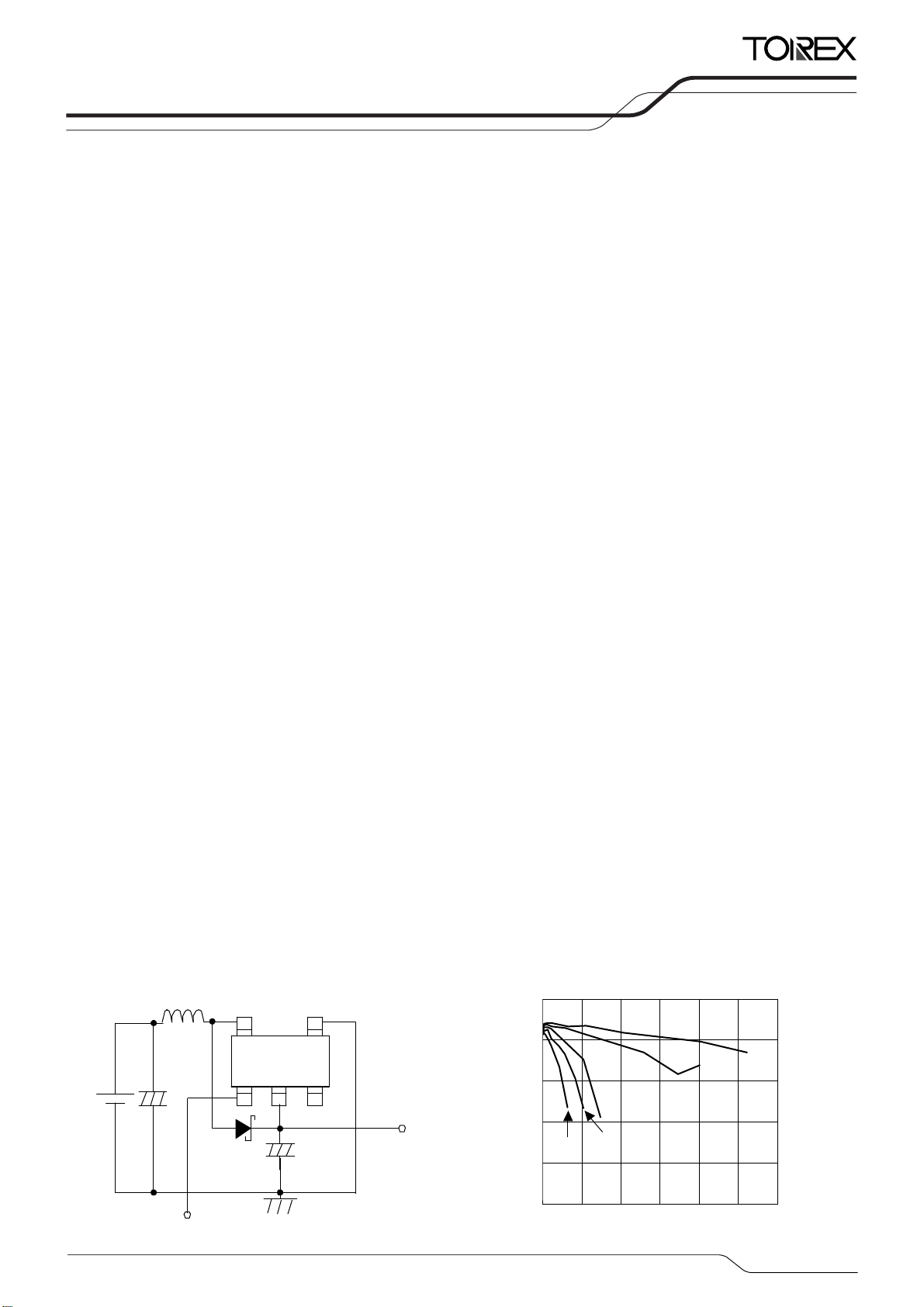
■TYPICAL APPLICATION CIRCUIT
●C type circuit
54
(TOP VIEW)
SOT-25
23
1
+
SD
CL
(Tantalum)
GND
VOUT
VIN
L
CIN
+
CE
■TYPICAL PERFORMANCE
CHARACTERISTICS
C9111E331MR
L=100μH(CR54), CL47μF(Tantalum)
80
60
40
Effic iency: EFFI(% )
VIN=0.9V
20
0
0 5 0 1 00 150 2 00 250 3 00
1.5V
1.2V
Output Current:IOUT(mA)
SD: XBS104S14R-G
2.4V
3.0V
1/36
XC9110/XC9111 Series
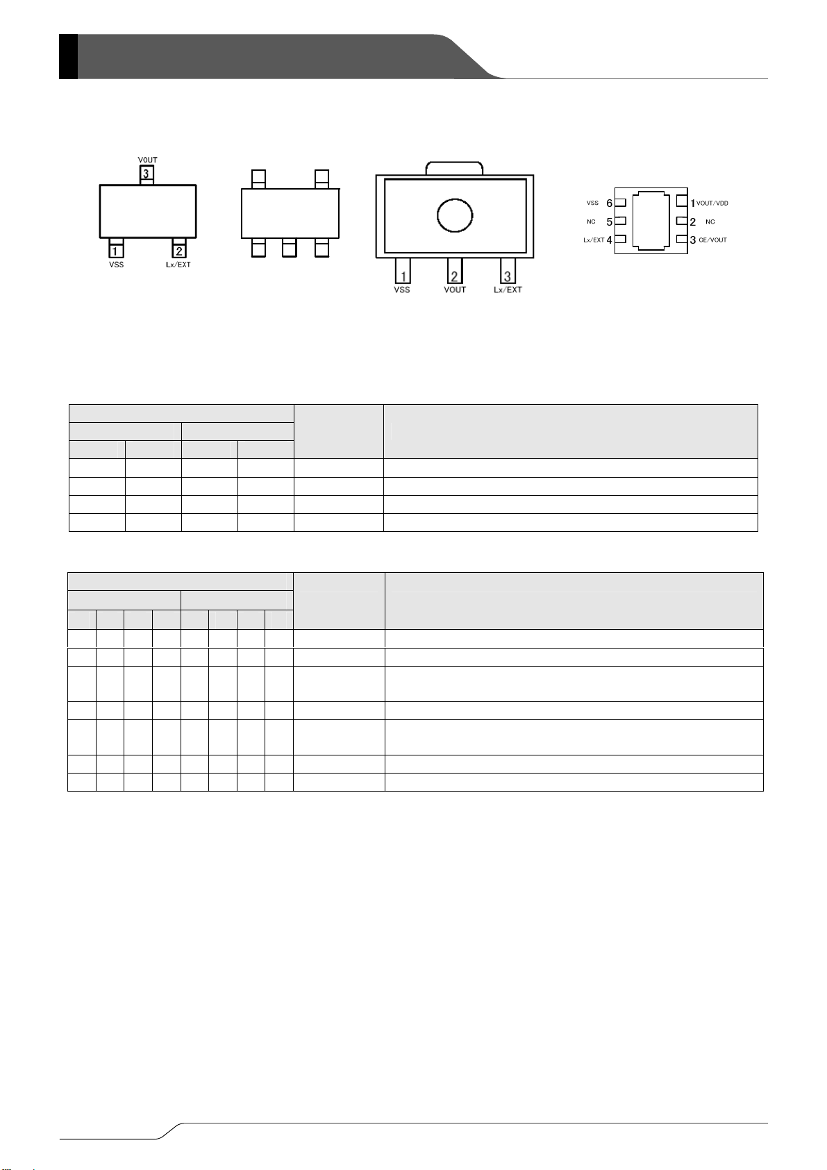
■PIN CONFIGURATION
SOT-23 (TOP VIEW)
■PIN ASSIGNMENT
●
XC9111A/B
Lx/EXT
54
123
CE/V OUT
V OUT/V DD
SOT-25 (TOP VIEW)
PIN NUMBER
SOT-23 SOT-89
A B A B
1 1 1 1 VSS Ground
3 3 2 2 VOUT Output Voltage Montior, Internal Power Supply
2 - 3 - LX Switch
- 2 - 3 EXT External Switching transistor drive <N-ch transistor drive)
●XC9110//9111C/D/E/F
PIN NUMBER
SOT-25 USP-6C
C D E F C D E F
- - 2 2 - - 1 1 VDD Internal Power Supply
4 4 4 4 6 6 6 6 VSS Ground
- 5 - 5 - 4 - 4 EXT
5 - 5 - 4 - 4 - Lx Switch
1 1 - - 3 3 - - CE
2 2 1 1 1 1 3 3 VOUT Output voltage monitor
3 3 3 3 2,5 2,5 2,5 2,5 NC No connection
VSS
NC
USP-6C (BOTTOM VIEW)
SOT-89 (TOP VIEW)
*The dissipation pad for the USP-6C package
should be solder-plated in recommended mount
pattern and metal masking so as to enhance
mounting strength and heat release. If the pad
needs to be connected to other pins, it should be
connected to the pin No.1.
PIN NAME FUNCTIONS
PIN NAME FUNCTIONS
External switching transistor drive
<Connect to the gate pin of N-ch Power MOSFET>
Chip Enable <Connect to the V
OUT pin when Active and the
VSS pin when stand-by>
2/36
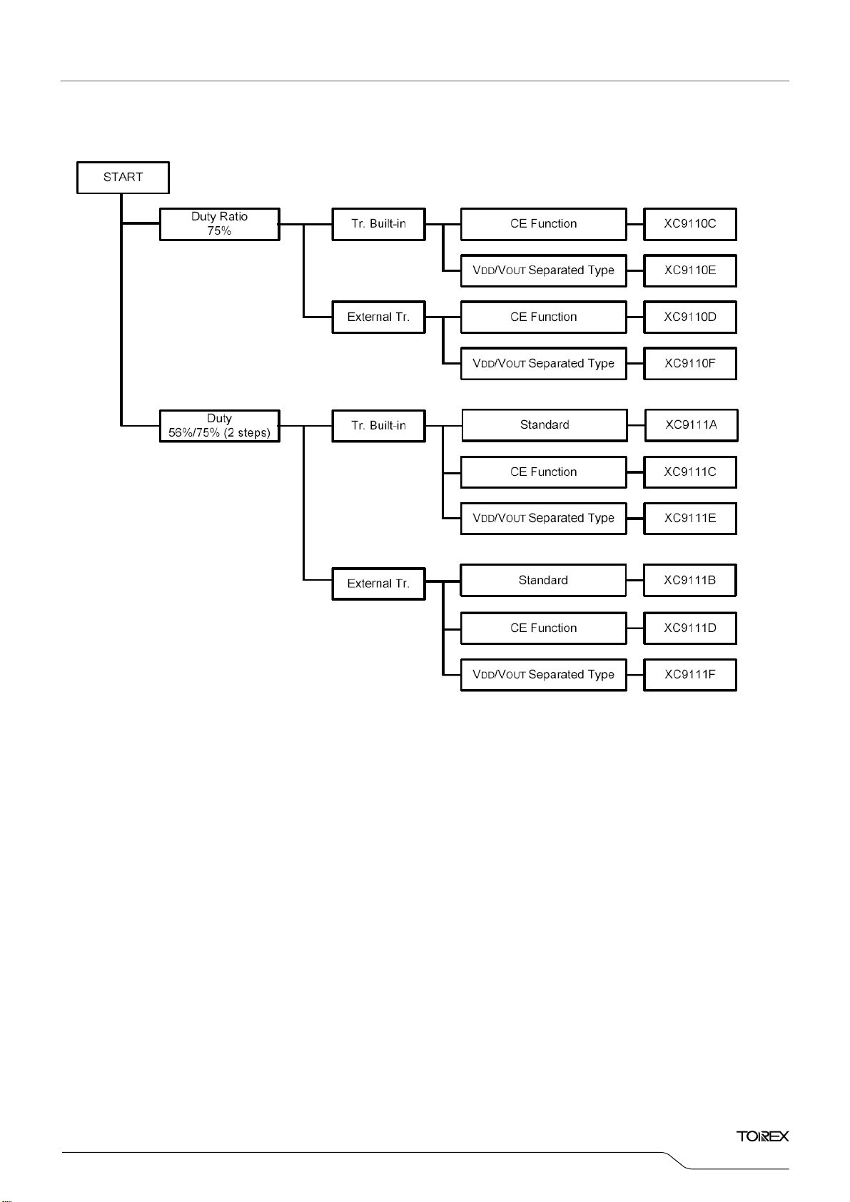
■PRODUCT CLASSIFICATION
●Selection Guide
XC9110/XC9111
Series
3/36
XC9110/XC9111 Series
■PRODUCT CLASSIFICATION
●Ordering Information
XC9110①②③④⑤⑥-⑦ : PFM control, 75% duty
XC9111①②③④⑤⑥-⑦
DESIGNATOR ITEM SYMBOL DESCRIPTION
①
②③
④
⑤⑥-⑦
(*1)
The “-G” suffix denotes Halogen and Antimony free as well as being fully RoHS compliant.
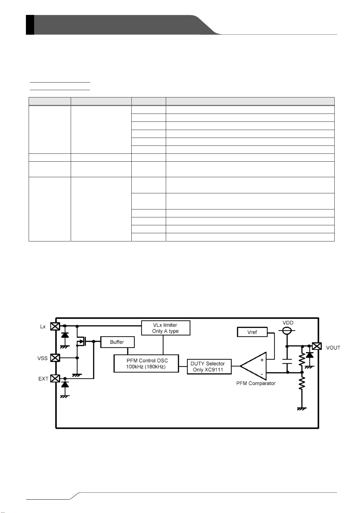
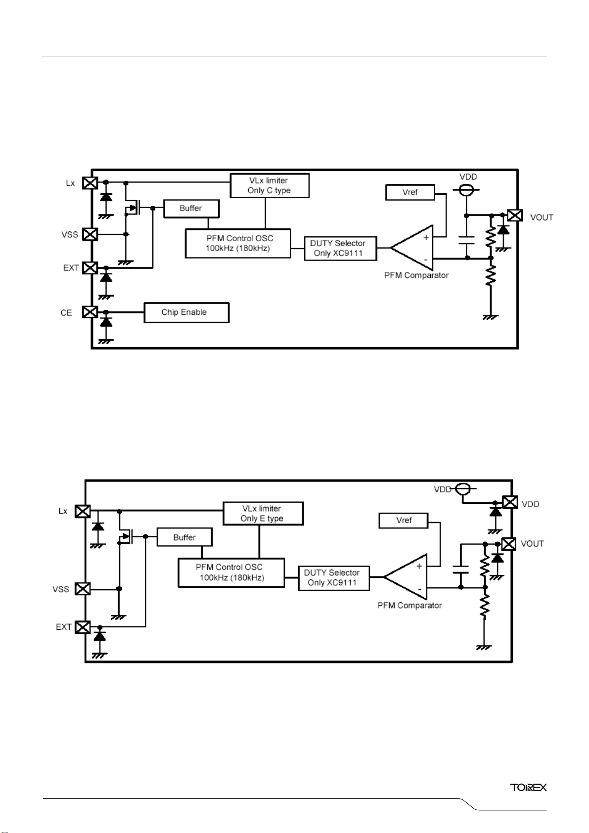
■BLOCK DIAGRAMS
●XC9111 A and B series
(*1)
Note: The XC9110 series, Tr. Built-in type, uses the Lx pin and the XC9111 series, external Tr. Type, uses the EXT pin.
The duty ratio of the XC9111 series automatically varies between 56% (oscillation frequency 180kHz) and 75%
(oscillation frequency (f
* The duty ratio depends on power supply. Please refer to the electrical characteristics on duty against output voltage
you use.
: PFM control, 56% / 75% duty variable
A VDD / V
B VDD / V
CE Function
C CE pin (5 pin) Built-in Transistor
D CE pin (5 pin) External Transistor
E VDD / V
F V
Output Voltage 15 ~ 70
Maximum Oscillation
Frequency
1 100kHz
MR
Packages
(Order Unit)
MR-G
PR
PR-G
ER
ER-G
) 100kHz). The VLx limit function only applies to the XC9110/9111 A types.
OSC
common type (for XC9111series) Built-in Transistor
OUT
common type (for XC9111series) External Transistor
OUT
separated type (5 pin) Built-in Transistor
OUT
/ V
DD
separated type (5 pin) External Transistor
OUT
ex. 3.5V output → ②= 3, ③= 5
①=A~B SOT-23 (3,000/Reel)
①=C~F SOT-25 (3,000/Reel)
①=A~B SOT-23 (3,000/Reel)
①=C~F SOT-25 (3,000/Reel)
①=A~B SOT-89 (1,000/Reel)
①=A~B SOT-89 (1,000/Reel)
①=C~F USP-6C (3,000/Reel)
①=C~F USP-6C (3,000/Reel)
4/36
■BLOCK DIAGRAMS
●XC9110 / 9111 C and D series
Note: The XC9110 series, Tr. Built-in type, uses the Lx pin and the XC9111 series, external Tr. Type, uses the EXT pin.
The XC9110 series' duty ratio is 75% and oscillation frequency (f
automatically varies between 56% (oscillation frequency 180kHz) and 75% (oscillation frequency (f
V
Lx limit function only applies to the XC9110/9111 C versions.
* The duty ratio depends on power supply. Please refer to the electrical characteristics on duty against output voltage
you use.
●XC9111 E and F series
Note: The XC9110 series, Tr. Built-in type, uses the Lx pin and the XC9111 series, external Tr. Type, uses the EXT pin.
The XC9110 / 9111 series E and F series have the V
oscillation frequency (f
56% (oscillation frequency 180kHz) and 75% (oscillation frequency (f
The V
Lx limit function only applies to the XC9110/9111 C versions.
* The duty ratio depends on power supply.
Please refer to the electrical characteristics on duty against output voltage you use.
) is 100kHz. The duty ratio of the XC9111 series
OSC
) is 100kHz. The duty ratio of the XC9111 series automatically varies between
OSC
DD pin. The XC9110 series' duty ratio is 75% and
) 100kHz).
OSC
) 100kHz). The
OSC
XC9110/XC9111
Series
5/36
XC9110/XC9111 Series
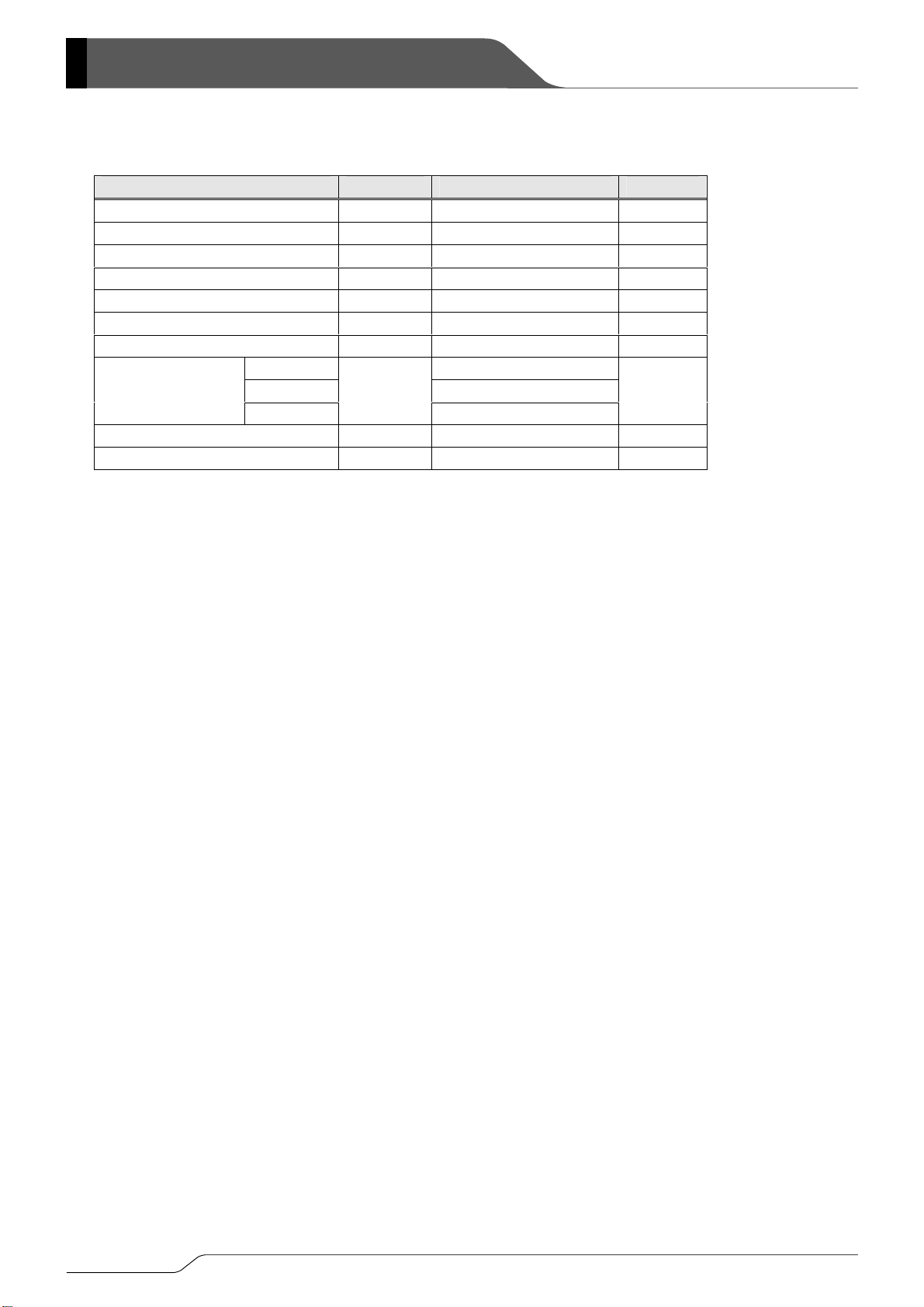
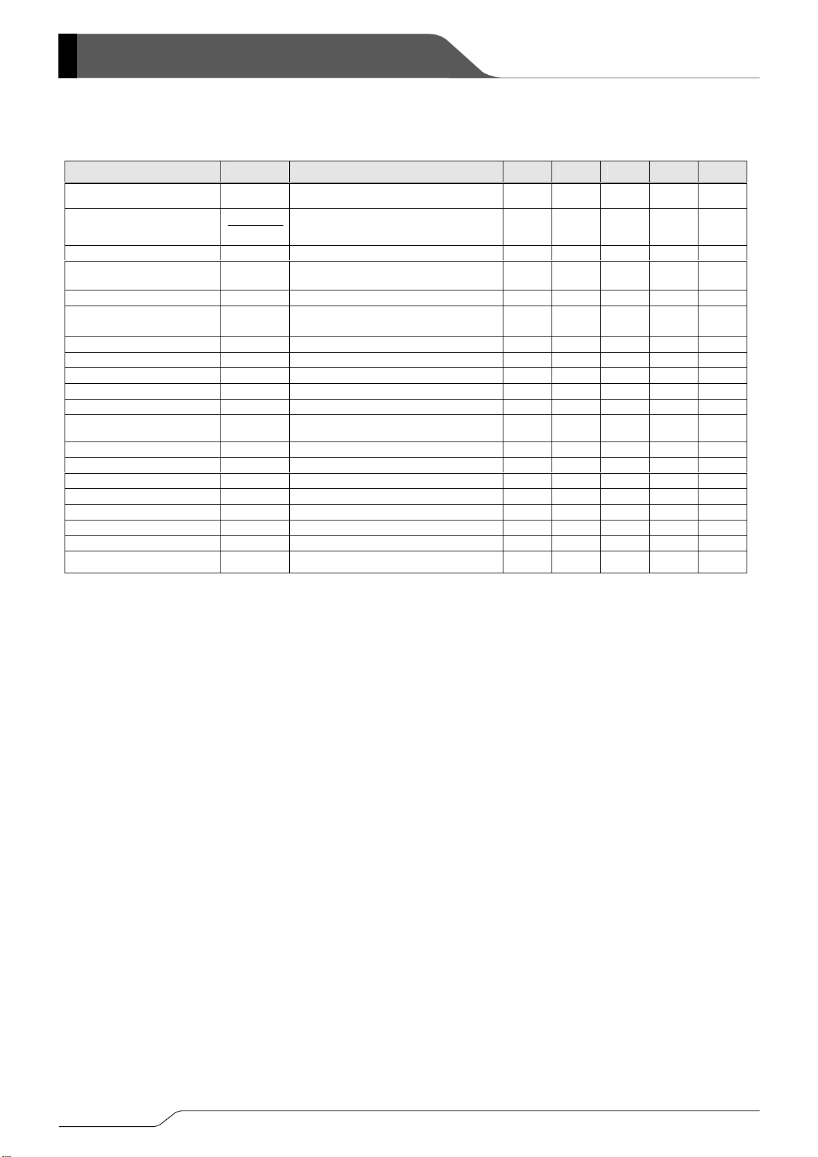
■ELECTRICAL CHARACTERISTICS
PAR AMETER SYMBOL RATINGS UNITS
VOUT Input Voltage VOUT – 0.3 ~ 12.0 V
Lx Pin Voltage VLx – 0.3 ~ 12.0 V
Lx Pin Current ILx 400 mA
EXT Pin Voltage VEXT VSS – 0.3 ~ VOUT+0.3 V
EXT Pin Current IEXT ±100 mA
CE Input Voltage VCE – 0.3 ~ 12.0 V
VDD Input Voltage VDD – 0.3 ~ 12.0 V
SOT-23, 25 250
Power Dissipation
SOT-89 500
USP-6C
Operating Ambient Temperature Topr – 40 ~ + 85 ℃
Storage Temperature Tstg – 55 ~ +125 ℃
Pd
* Define as VSS with a standard of all the voltage.
120
mW
6/36
XC9110/XC9111
Series
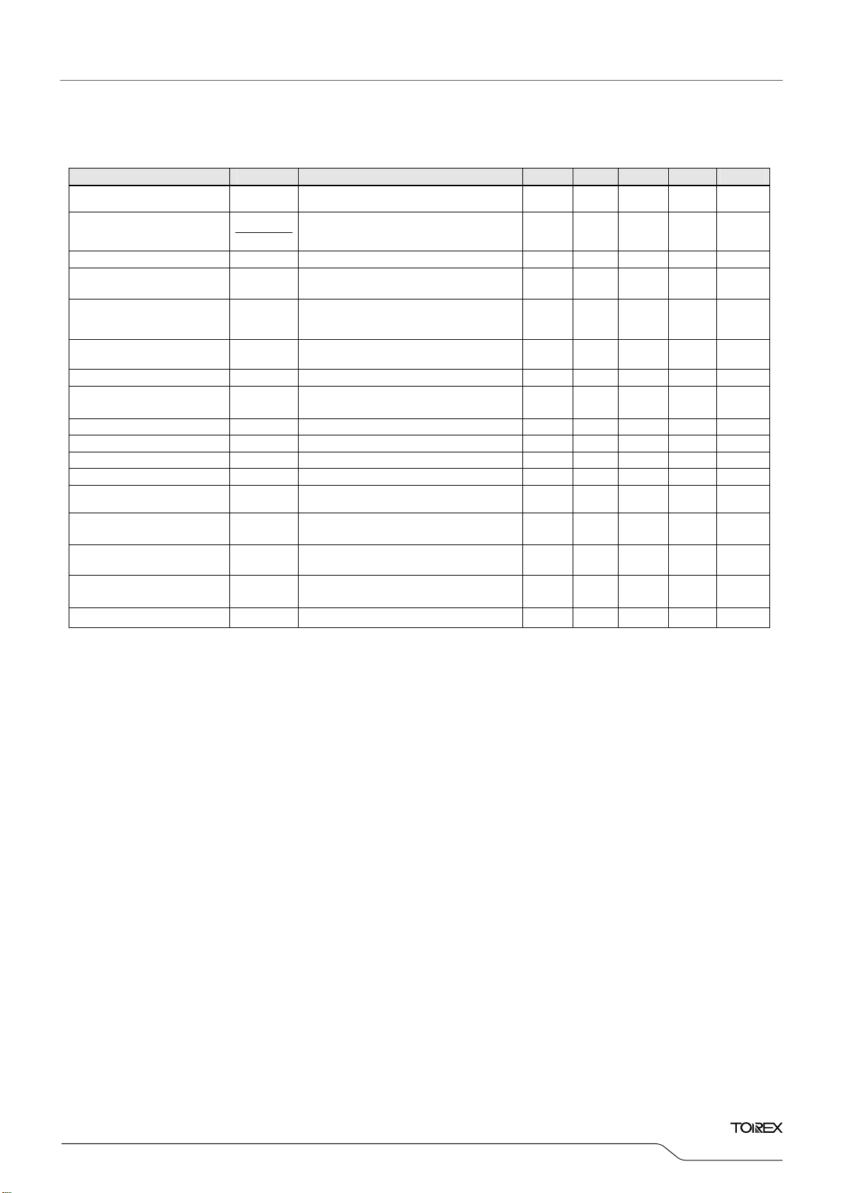
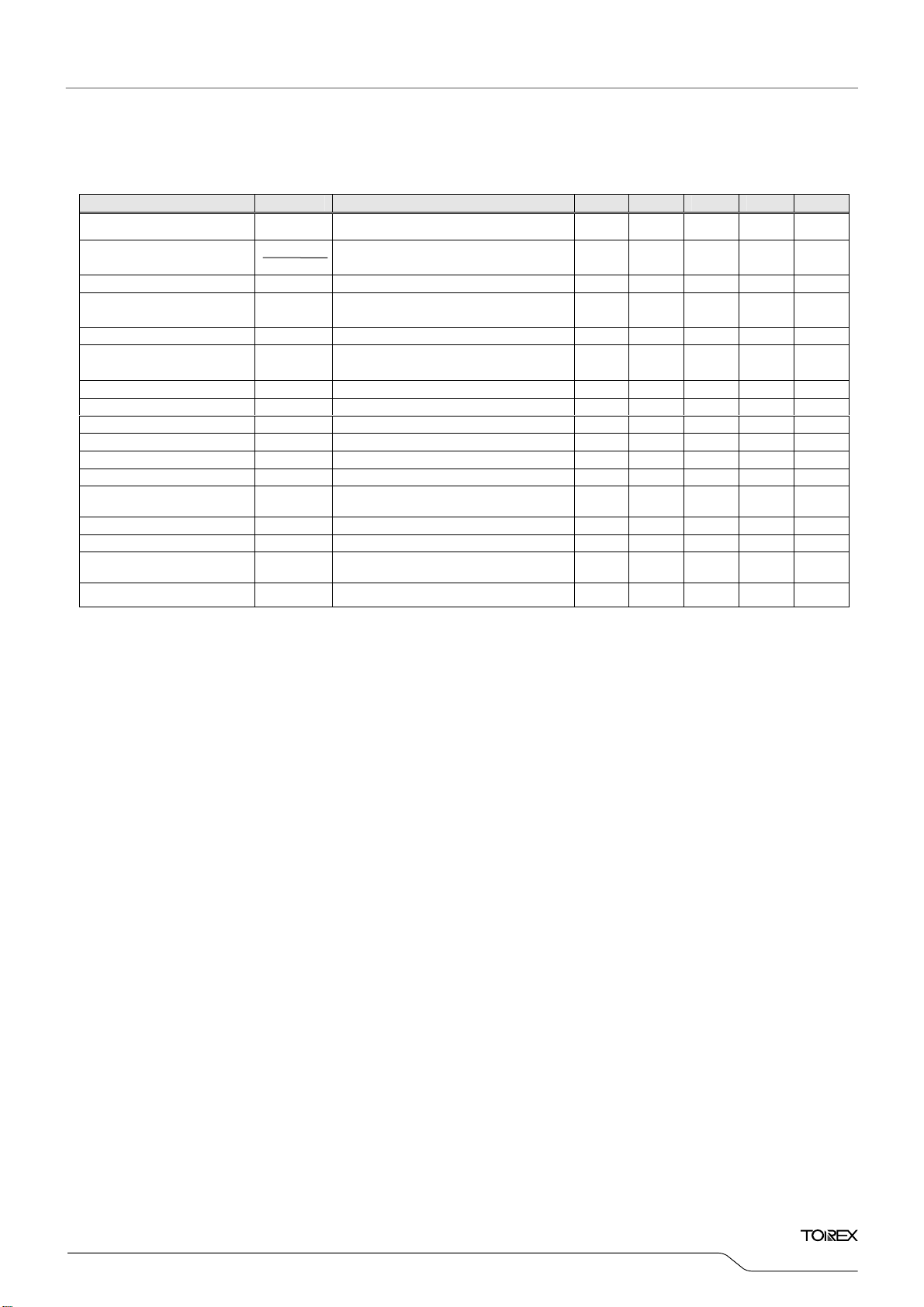
■ ABSOLUTE MAXIMUM RATINGS
XC9111Axx1MR
PARAMETER SYMBOL CONDITIONS MIN. TYP. MAX. UNIT
Output Voltage VOUT Connected to external components ×0.975 VOUT ×1.025 V ①
Output Voltage Temperature
Characteristics
△VOUT
△
V
OUT
・△
topr
Connected to external components
- 40℃≦Topr≦85℃
- ±100 -
Maximum Input Voltage VIN 10 - - V ①
Operating Start Voltage VST1
OUT=1mA,
Connected to external components
- 0.8 0.9 V ①
I
Oscillation Start Voltage VST2 Applied 0.8V to VOUT, Vpull=1.0V - - 0.8 V ②
Operating Hold Voltage VHLD
OUT=1mA,
Connected to external components
0.7 - - V ①
I
Input Current at No Load IIN IOUT=0mA (*1) - E1-1(*) E1-2(*) μA ①
Supply Current 1 (*2) IDD1 Applied (output voltage×0.95) to VOUT - E2-1(*) E2-2(*) μA ②
Supply Current 2 IDD2 Applied (output voltage+0.5) to VOUT - E3-1(*) E3-2(*) μA ②
Lx Switch ON Resistance RSWON Same as IDD1, VLx=0.4V (*3) - E4-1(*) E4-2(*) Ω ②
Lx Leak Current ILxL Same as IDD2, VLx=7V - - 1 μA ③
Duty Ratio DTY Same as IDD1, measure Lx waveform E7-1(*) E7-2(*) E7-3(*) % ②
Duty Ratio 2 DTY2
Maximum Oscillation
Frequency
Maximum Oscillation
Frequency 2
MAXf
MAXf
Lx Limit Voltage (*4) VLxLMT
I
Connect to external components
Same as IDD1 85 100 115 kHz ②
OSC
Same as IDD1 153 180 207 kHz ②
OSC2
Same as I
DD1, VLx when max. oscillation
frequency is more than double
48 56 64 % ①
0.7 - 1.1 V ②
OUT=1mA, measure Lx ON time.
Efficiency (*5) EFFI Connect to external components - E8(*) - % ①
Test condition : Unless otherwise specified, V
NOTE:
*1: TOREX SBD, XBS104S14R-G is used, reverse current IR < 1μA (when reverse voltage V
parts.
*2: Supply Current 1 is the value when the IC is constantly switching. In actual operation, the oscillator periodically switches, resulting in
lower power consumption. Please refer to Input Current (I
input power supply (V
*3: Lx switch ON resistance can be calculated by (V
*4: The Lx limit voltage function becomes stable when V
*5: EFFI={[output voltage]×(output current)} / [(input voltage)×(input current)]×100
IN).
IN=VOUT×0.6, IOUT=<C1(*)>, Vpull=5.0V
R = 10V is applied), in case of using selected
IN) under no load condition for the actual current, which is supplied from the
Lx x Rp) / (Vpull - VLx). * Change Vpull so that VLx will become 0.4V.
OUT is over 2.0V.
*6: Please be aware of the absolute maximum ratings of the external components.
(*): Please refer to the charts.
ppm/
℃
Ta = 2 5 ℃
CIRCUIT
①
7/36

XC9110/XC9111 Series
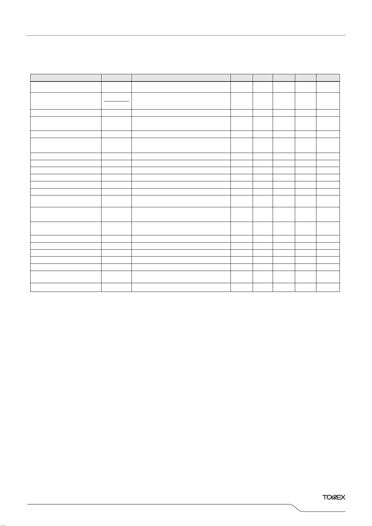
■ELECTRICAL CHARACTERISTICS (Continued)
XC9111Bxx1MR
PARAMETER SYMBOL CONDITIONS MIN. TYP. MAX. UNIT
Output Voltage VOUT Connected to external components ×0.975 VOUT ×1.025 V ⑥
Output Voltage
Temperature Characteristics
Maximum Input Voltage VIN 10 - - V -
Operating Start Voltage VST1
Oscillation Start Voltage VST2 Applied 0.8V to VOUT - - 0.8 V ⑦
Operation Hold Voltage VHLD
Supply Current 1 (*1) IDD1 Applied (output voltage×0.95) to VOUT - E2-1(*) E2-2(*) μA ⑦
Supply Current 2 IDD2 Applied (output voltage+0.5) to VOUT - E3-1(*) E3-2(*) μA ⑦
EXT ‘H’ ON Resistance
EXT ‘L’ ON Resistance
Duty Ratio DTY Same as IDD1, measure Lx waveform E7-1(*) E7-2(*) E7-3(*) % ⑦
Duty Ratio 2 DTY2
Maximum Oscillation
Frequency
Maximum Oscillation
Frequency 2
Efficiency (*4) EFFI Connect to external components - E9(*) - % ⑥
Test condition : Unless otherwise specified, VIN=VOUT×0.6, IOUT=<C1(*)>
NOTE:
*1: Supply Current 1 is the value when the IC is constantly switching. In actual operation, the oscillator periodically switches, resulting in
lower power consumption.
*2: EXT ‘H’ ON resistance can be calculated by (0.4 x Rp) / ( V
*3: EXT ‘L’ ON resistance can be calculated by (V
*4: EFFI={[output voltage]×(output current)} / [(input voltage)×(input current)]×100
*5: Please be aware of the absolute maximum ratings of the external components.
(*): Please refer to the charts.
△VOUT
△
V
OUT
・△topr
R
EXTH Same as IDD1, VEXT=VOUT-0.4V (*2) - E5-1(*) E5-2(*) Ω ②
R
EXTL Same as IDD1, VEXT=0.4V (*3) - E6-1(*) E6-2(*) Ω ②
MAXf
OSC
MAXf
OSC2
Connected to external components
Same as IDD1 85 100 115 kHz ⑦
Same as IDD1 153 180 207 kHz ⑦
- 40℃≦Topr≦85℃
I
OUT=1mA, Connected to external
components
I
OUT=1mA,
Connected to external components
I
OUT=1mA, measure Lx ON time.
Connect to external components
EXT – Vpull). * Change Vpull so that VEXT will become VOUT-0.4V.
EXT x Rp) / ( Vpull- VEXT). * Change Vpull so that VEXT will become 0.4V.
- ±100 -
- 0.8 0.9 V ⑥
0.7 - - V ⑥
48 56 64 % ⑥
ppm/
℃
Ta = 2 5 ℃
CIRCUIT
⑥
8/36
XC9110/XC9111
Series
■ELECTRICAL CHARACTERISTICS (Continued)
XC9110Cxx1MR, XC9111Cxx1MR
PARAMETER SYMBOL CONDITIONS MIN. TYP. MAX. UNIT CIRCUIT
Output Voltage VOUT Connect to external components ×0.975 VOUT ×1.025 V ①
Output Voltage
Temperature Characteristics
△VOUT
△VOUT・△topr
Connect to external components
- 40℃≦Topr≦85℃
- ±100 -
Maximum Input Voltage VIN 10 - - V ①
Operation Start Voltage VST1
OUT=1mA, connect to external
components
- 0.8 0.9 V ①
I
Oscillation Start Voltage VST2 Applied 0.8V to VOUT, Vpull=1.0V - - 0.8 V ②
Operation Hold Voltage VHLD
OUT=1mA, connect to external
components
0.7 - - V ①
I
Input Current IIN IOUT=0mA (*1) - E1-1(*) E1-2(*) μA ①
Supply Current 1 (*2) IDD1 Applied (output voltage×0.95) to VOUT - E2-1(*) E2-2(*) μA ②
Supply Current 2 IDD2 Applied (output voltage+0.5V) to VOUT - E3-1(*) E3-2(*) μA ②
Lx Switch ON Resistance RSWON Same as IDD1, VLx=0.4V (*3) - E4-1(*) E4-2(*) Ω ②
Lx Leak Current ILxL Same as IDD2, VLx=7V - - 1 μA ③
Duty Ratio DTY Same as IDD1, measure Lx waveform E7-1(*) E7-2(*) E7-3(*) % ②
Duty Ratio 2 DTY2
Maximum
Oscillation Frequency
Maximum
Oscillation Frequency 2
MAXf
MAXf
I
only) Connect to external components
Same as IDD1 85 100 115 kHz ②
OSC
Same as IDD1 (XC9111 only) 153 180 207 kHz ②
OSC2
48 56 64 % ①
OUT=1mA, measure Lx ON time (XC9111
Stand-by Current ISTB Same as IDD1, VCE=0V - - 0.50 μA ④
CE “High” Voltage VCEH Same as IDD1, determine Lx oscillation 0.75 - - V ④
CE “Low” Voltage VCEL Same as IDD1, determine Lx shut-down - - 0.20 V ④
CE “High” Current ICEH Same as IDD1, VCE=VOUT×0.95 - - 0.25 μA ⑤
CE “Low” Current ICEL Same as IDD1, VCE=0V - - -0.25 μA ⑤
Lx Limit Voltage (*4) VLxLMT
Same as I
DD1, when max. oscillation
frequency is more than double.
0.7 - 1.1 V ②
Efficiency (*5) EFFI Connect to external components - E8(*) - % ①
Test condition : Unless otherwise specified, connect CE to VOUT, VIN=VOUT×0.6, IOUT=<C1(*)>, Vpull=5.0V
NOTE:
*1: TOREX SD, XBS104S14R-G is used, reverse current IR < 1μA (when reverse voltage V
parts.
*2: Supply Current 1 is the value when the IC is constantly switching. In actual operation, the oscillator periodically switches, resulting in
lower power consumption. Please refer to Input Current (I
input power supply (V
*3: Lx switch ON resistance can be calculated by (V
*4: The Lx. limit voltage function becomes stable when V
*5: EFFI={[output voltage]×(output current)} / [(input voltage)×(input current)]×100
IN).
Lx x Rp) / (Vpull - VLx). * Change Vpull so that VLx will become 0.4V.
IN) under no load condition for the actual current, which is supplied from the
OUT of the XC9110/9111 series is over 2.0V.
R = 10V is applied), in case of using selected
*6: Please be aware of the absolute maximum ratings of the external components.
(*): Please refer to the charts.
ppm/
℃
Ta = 2 5 ℃
①
9/36
XC9110/XC9111 Series
■ELECTRICAL CHARACTERISTICS (Continued)
XC9110Dxx1MR, XC9111Dxx1MR
PARAMETER SYMBOL CONDITIONS MIN. TYP. MAX. UNIT CIRCUIT
Output Voltage VOUT Connect to external components ×0.975 VOUT ×1.025 V ⑥
Output Voltage
Temperature Characteristics
Maximum Input Voltage VIN 10 - - V -
Operation Start Voltage VST1
Oscillation Start Voltage VST2 Applied 0.8V to VOUT - - 0.8 V ⑦
Operation Hold Voltage VHLD
Supply Current 1 (*1) IDD1 Applied (output voltage×0.95) to VOUT - E2-1(*) E2-2(*) μA ⑦
Supply Current 2 IDD2 Applied (output voltage+0.5V) to VOUT - E3-1(*) E3-2(*) μA ⑦
EXT H ON Resistance REXTH Same as IDD1, VEXT=VOUT-0.4(*2) - E5-1(*) E5-2(*) Ω ②
EXT L ON Resistance REXTL Same as IDD1, VEXT=0.4V(*3) - E6-1(*) E6-2(*) Ω ②
Duty Ratio DTY Same as IDD1, measure Lx waveform E7-1(*) E7-2(*) E7-3(*) % ⑦
Duty Ratio 2 DTY2
Maximum Oscillation
Maximum Oscillation
Standby Current ISTB Same as IDD1, VCE=0V - - 0.50 μA ⑤
CE “High” Voltage VCEH Same as IDD1, determine Lx oscillation 0.75 - - V ⑧
CE “Low” Voltage VCEL Same as IDD1, determine Lx shut-down - - 0.20 V ⑧
CE “High” Current ICEH Same as IDD1, VCE=VOUT×0.95 - - 0.25 μA ⑤
CE “Low” Current ICEL Same as IDD1, VCE=0V - - -0.25 μA ⑤
Efficiency (*4) EFFI Connect to external components - E9(*) - % ⑥
Test condition : Unless otherwise specified, connect CE to VOUT, VIN=VOUT×0.6, IOUT=<C1(*)>
NOTE:
*1: "Supply Current 1" is the value when the IC is constantly switching. In actual operation, the oscillator periodically switches, resulting in lower
power consumption.
*2: EXT H ON resistance can be calculated by (0.4 x Rp) / (V
*3: EXT L ON resistance can be calculated by (V
*4: EFFI={[output voltage]×(output current)} / [(input voltage)×(input current)]×100
*5: Please be aware of the absolute maximum ratings of the external components.
(*): Please refer to the charts.
△VOUT
△VOUT・△topr
MAXf
MAXf
Same as IDD1 85 100 115 kHz ⑦
OSC
OSC2
Connect to external components
- 40℃≦Topr≦85℃
I
OUT=1mA, connect to external
I
OUT=1mA, connect to external
OUT=1mA, measure Lx ON time (XC9111
I
only) Connect to external components
Same as IDD1 (XC9111 only) 153 180 207 kHz ⑦
EXT x Rp) / (Vpull - VEXT). * Change Vpull so that VEXT will become 0.4V.
components
components
EXT - Vpull). * Change Vpull so that VEXT will become VOUT-0.4V.
- ±100 -
- 0.8 0.9 V ⑥
0.7 - - V ⑥
48 56 64 % ⑥
ppm/
℃
Ta = 2 5 ℃
⑥
10/36
XC9110/XC9111
Series
■ELECTRICAL CHARACTERISTICS (Continued)
XC9110Exx1MR, XC9111Exx1MR
PARAMETER SYMBOL CONDITIONS MIN. TYP. MAX. UNIT CIRCUIT
Output Voltage VOUT Connect to external components ×0.975 VOUT ×1.025 V ①
Output Voltage
Temperature Characteristics
△V
OUT
△VOUT・△topr
Maximum Input Voltage VIN 10 - - V -
Operation Start Voltage VST1
Oscillation Start Voltage VST2 Applied 0.8V to VOUT, Vpull=1.0V - - 0.8 V ②
Operation Hold Voltage VHLD
Input Current IIN IOUT=0mA (*1) - E1-1(*) E1-2(*) μA ①
Supply Current 1 (*2) IDD1 Applied (output voltage×0.95) to VOUT - E2-1(*) E2-2(*) μA ②
Supply Current 2 IDD2 Applied (output voltage+0.5V) to VOUT - E3-1(*) E3-2(*) μA ②
Lx Switch ON Resistance RSWON Same as IDD1, VLx=0.4V (*3) - E4-1(*) E4-2(*) Ω ②
Lx Leak Current ILxL Same as IDD2, VLx=7V - - 1 μA ③
Duty Ratio DTY Same as IDD1, measure Lx waveform E7-1(*) E7-2(*) E7-3(*) % ②
Duty Ratio 2 DTY2
Maximum Oscillation
Maximum Oscillation
MAXf
MAXf
OSC
OSC2
Lx Limit Voltage (*4) VLxLMT
Efficiency (*5) EFFI Connect to external components - E8(*) - % ①
Test condition : Unless otherwise specified, connect VDD to VOUT, VIN=VOUT×0.6, IOUT=<C1(*)>, Vpull=5.0V
NOTE:
*1: TOREX SD, XBS104S14R-G is used; reverse current IR < 1μA (when reverse voltage V
selected parts.
*2: "Supply Current 1" is the value when the IC is constantly switching. In actual operation, the oscillator periodically switches, resulting
in lower power consumption. Please refer to Input Current (I
from the input power supply (V
IN).
*3: Lx switch ON resistance can be calculated by (V
*4: The Lx limit voltage function becomes stable when V
*5: EFFI={[output voltage]×(output current)} / [(input voltage)×(input current)]×100
*6: When using V
The IC operates from V
DD and VOUT separately, please set the voltage range of VDD from 1.5V to 10V.
DD=0.8V, but output voltage and oscillation frequency will be stable when VDD=1.5V or more.
*7: Please be aware of the absolute maximum ratings of the external components.
(*): Please refer to the charts.
Connect to external components
- 40℃≦Topr≦85℃
I
OUT=1mA, connect to external
components
I
OUT=1mA, connect to external
components
OUT=1mA, measure Lx ON time (XC9111
I
only) Connect to external components
- ±100 -
- 0.8 0.9 V ①
0.7 - - V ①
48 56 64 % ①
Same as IDD1 85 100 115 kHz ②
Same as IDD1 (XC9111 only) 153 180 207 kHz ②
Same as I
DD1, VLx when max. oscillation
frequency is more than double.
IN) under no load condition for the actual current, which is supplied
Lx x Rp) / (Vpull - VLx). * Change Vpull so that VLx will become 0.4V.
OUT of the XC9110/9111 series is over 2.0V.
0.7 - 1.1 V ②
R = 10V is applied), in case of using
ppm/
℃
Ta = 2 5 ℃
①
11/36
 Loading...