

Torex XC9106, XC9107 User Manual
A
H
F
T
F
XC9106/XC9107 Series
ETR0405_004
PWM Control, PWM/PFM Switching Control,
Step-Up DC/DC Converters, Externally Applied Vref
■GENERAL DESCRIPTIO N
The XC9106 / XC9107 series are step-up DC/DC controller ICs with an externally applied reference voltage (Vref).
Output voltage will be set with external resistors (R
voltage externally and are suited to software applications that need to vary voltage, such as LCD power supply for PDA.
Output will be stable no matter which load capacitors are used but if a low ESR capacitor is used, RSENSE of about 0.1Ω will
be required and phase compensation will be achieved. This makes the use of ceramic capacitors much easier, and allows for
lower output ripple and reduced PCB area requirements. Tantalum and electrolytic capacitors can also be used, in which
case, R
Oscillation frequencies of high clock, low ripple 300kHz and low supply current 100kHz are available.
The XC9107 series are PWM/PFM automatic switching controlled. Control switches from PWM to PFM during light loads with
the XC9107 and the series is highly efficient from light loads to large output currents. By bringing the whole circuit down
while the series is in the stand-by mode (CE/PWM pin: low), supply current can be reduced to less than 1.0μA.
SENSE becomes unnecessary.
FB1 and 2) and Vref value. The series make it easy to control output
■
PPLICATIONS
●Power supply for LCDs
●PDAs
●Cellular phones
●Palmtop computers
●Portable audio systems
●Various multi-function power supplies
■FEATURES
Input Voltage : 0.9V ~ 10V
Power
Supply Voltage Range : 1.8V~10.0V and more than
VREF Input Range : 0.8V~2.5V (±2.0%)
Output Voltage : Vref x external split resistor ratio
Oscillation Frequency : 300kHz, 100kHz (±15%)
Output Current : More than 30mA
(V
Controls : PWM (XC9106)
: PWM/PFM auto-switching
High Efficiency : 85% (TYP.)
Stand-by Current : ISTB = 1.0μA (MAX.)
Load Capacitors : Low ESR capacitors compatible
Externally Applied Reference Voltage (Vref)
Packages : SOT-25, USP-6B
Environmentally Friendly
■
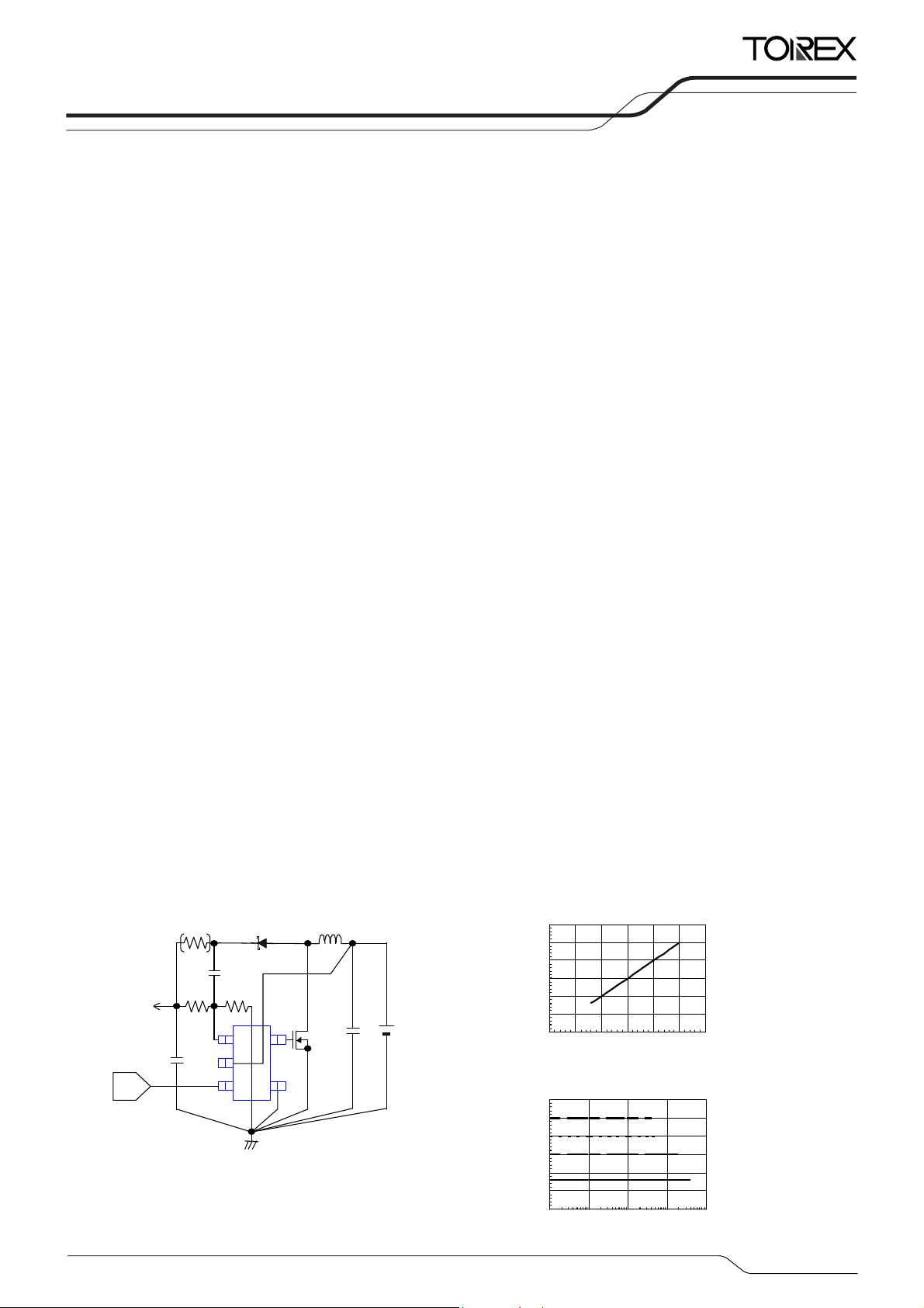
TYPICAL APPLICATION CIRCUIT
V
OUT
= 8V~25V
= 30mA
I
OUT
Ceramic CL :
10
μ
0.8V~2.5V
D/A converter
RSENSE : 10 0m
for Ceramic CL
*
RFB1 :
270k
Ω
CE/Vref
Ω
SD : MA737
CFB : 27p
RFB2 :
30k
Ω
15
2
3
4
L : 10
Nch Pow er
MOS FE
2SK2159
μ
CIN
* RSENSE is of no use in light load (uncontinuous mode)
applications such as a small LCD, even using ceramic
capacitor.
V
= 3.3V
IN
■TYPICAL PERFORMANCE
CHARACTERISTICS
XC9107D003MR
V
30
25
20
(V)
15
OUT
V
10
5
0
0.0 0.5 1.0 1.5 2.0 2.5 3.0
XC9107D003MR
30
25
20
(V)
15
OUT
V
10
5
0
0.1 1 10 100 1000
DD=VIN
☆GreenOperation-Compatible
Vref+0.7V
V
OUT=Vref x (RFB1+RFB2)/RFB2
IN=3.3V, VOUT=20V,
when external components are
used as in the circuits below.)
(XC9107)
: EU RoHS Compliant, Pb Free
Circuit as left
=3.3V, I
=30m A
OUT
Vref (V)
Circuit as left
=3.3V
V
DD=VIN
2.5V
2.0V
1.5V
Vref=0.8V
(mA)
I
OUT
1/11
XC9106/XC9107 Series
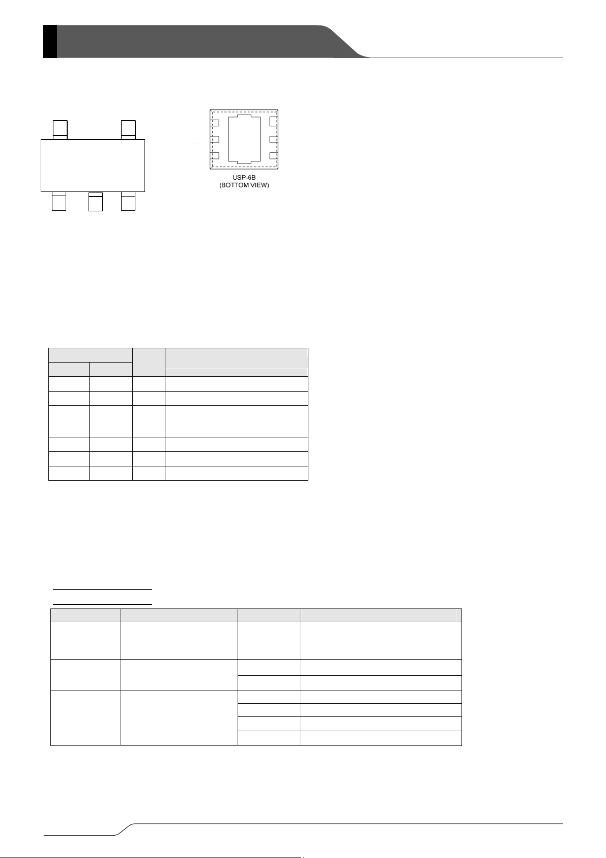
■PIN CONFIGURATION
NC
12
FB
■PIN ASSIGNMENT
VDD
SOT-25
(TOP VIEW)
PIN NUMBER
SOT-25 USP-6B
1 6 FB Output Resistor Connection
2 2 VDD Supply Voltage
3 4
4 3 GND Ground
5 1 EXT External Transistor Connection
- 5 NC No Connection
■PRODUCT CLASSIFICATION
●Ordering Information
XC9106D①②③④⑤-⑥
XC9107D①②③④⑤-⑥
DESIGNATOR ITEM SYMBOL DESCRIPTION
GND
45
3
CE/Vref
NAME
FB 6
NC 5
CE/VIEW
PIN
CE/
Serves as Both Chip Enable Pin
Vref
and Reference Voltage Apply Pin.
(*1)
: PWM control
(*1)
: PWM/PFM automatic switching control
FUNCTION
1 EXT
2 VDD
3
*The dissipation pad for the USP-6B package should be
solder-plated in recommended mount pattern and metal
masking so as to enhance mounting strength and heat
release. If the pad needs to be connected to other pins. it
should be connected to the V
DD pin.
①②
③
④⑤-⑥
(*1)
The “-G” suffix indicates that the products are Halogen and Antimony free as well as being fully RoHS compliant.
Reference Voltage
(Apply External)
Oscillation Frequency
Packages
(Oder Unit)
00 Fixed
3 300kHz
1 100kHz
MR
MR-G
DR
DR-G
SOT-25 (3,000/Reel)
SOT-25 (3,000/Reel)
USP-6B (3,000/Reel)
USP-6B (3,000/Reel)
2/11
A
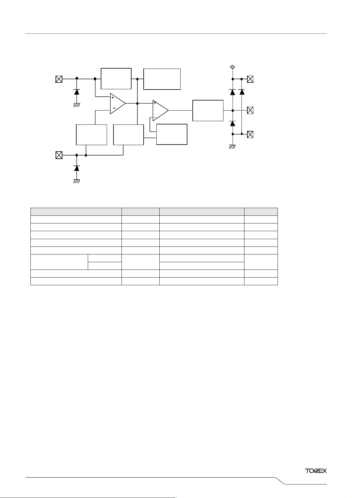
■BLOCK DIAGRAM
FB
Current
Ripple Detect
and FB
Error Amp.
Phase
Compensation
PWM
Comparator
Buffer,
Driver
XC9106/XC9107
Series
VDD
EXT
Vref with
Soft Start,
CE
CE / Vref
■
BSOLUTE MAXIMUM RATINGS
PARAMETER SYMBOL RATINGS UNITS
VDD pin Voltage VDD
FB Pin Voltage VFB
CE / Vref pin Voltage VCE / Vref
EXT pin Voltage VEXT
EXT pin Current IEXT/
Power Dissipation
SOT-25 150
USP-6B
Operating Temperature Range Topr
Storage Temperature Range Tstg
PWM/PFM
Controller
Pd
Ramp Wave
Generator,
OSC
FB, CE : CMOS INPUT
EXT : CMOS OUTPUT
-0.3~12.0
-0.3~12.0
-0.3~12.0
DD+0.3
-0.3~V
±100
100
-40~+85
-55~+125
GND
Ta = 25OC
V
V
V
V
mA
mW
O
C
O
C
3/11
XC9106/XC9107 Series
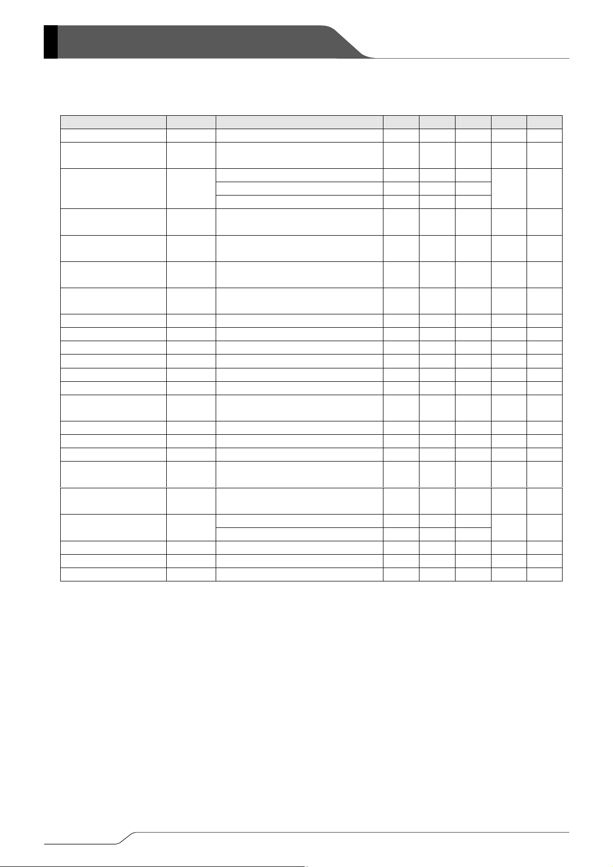
■ELECTRICAL CHARACTERISTICS
XC9106D001MR, XC9107D001MR
(FOSC=100kHz)
PARAMETER SYMBOL CONDITIONS MIN. TYP. MAX.
Output Voltage VOUT Vref = 0.9V 8.820 9.000 9.180 V
Reference
Voltage Range
Vref 0.8 - 2.5 V -
Vref = 0.8V 0.784 0.800 0.816
FB Control Voltage VFB
Vref = 0.9V 0.882 0.900 0.918
Vref = 2.5V 2.450 2.500 2.550
Supply Voltage Range
(*1)
V
DD
Operation Start Voltage VST1
Oscillation
Start Voltage (*1)
V
ST2
Operation Hold Voltage VHLD
CE/Vref=0.9V, V oltage applied, FB=0V
DD as shown right and
V
(Vref applied voltage+0.7V)
Recommended Circuit using
2SD1628, I
OUT=1.0mA
No external connections,
Recommended circuit using
2SD1628, I
OUT=1.0mA
1.8 - 10.0 V -
- - 0.9 V
- - 0.8 V
- - 0.7 V
Supply Current 1 IDD1 Same as VST2, VDD=3.300V - 29 41
Supply Current 2 IDD2 Same as IDD1, FB=1.2V - 14 19
Stand-by Current ISTB Same as IDD1, CE/Vref=0V - - 1.0
Oscillation Frequency FOSC Same as IDD1 85 100 115 kHz
Maximum Duty Ratio MAXDTY Same as IDD1 75 81 87 %
PFM Duty Ratio PFMDTY No Load (XC9106 series) 20 28 36 %
Efficiency EFFI
Recommended circuit using
XP161A1355
- 85 - %
Soft-start Time TSS Vref=0.9V 5.0 10.0 20.0 mS
CE “High” Voltage VCEH Same as IDD1 0.65 - - V
CE “Low” Voltage VCEL Same as IDD1 - - 0.20 V
EXT “High”
ON Resistance
EXT “Low”
ON Resistance
CE “High” Current ICEH
REXTH Same as IDD1, VEXT=VOUT-0.4V - 24 36
REXTL Same as IDD1, VEXT=0.4V - 16 24
Same as IDD2, CE=0.8V -1.0 - 0.0
Same as I
DD2, CE=2.5V 0.0 - 2.5
CE “Low” Current ICEL Same as IDD2, CE=0V - - -0.1
FB “High” Current IFBH Same as IDD2, FB=VDD - - 0.1
FB “Low” Current IFBL Same as IDD2, FB=1.0V - - -0.1
Test Conditions: Unless otherwise stated, CL: Ceramic, recommended MOSFET should be connected.
V
V
NOTE:
*1: Although the IC starts step-up operations from a V
V
DD ≧ 1.8V and (Vref applied voltage+0.7V). Therefore, a VDD of more than 1.8V and (Vref applied voltage+0.7V) is
recommended when V
DD= 3.3V → Vref= 0.09V, RFB1,2×10
IN= 3.3V → IOUT= 50mA
DD of 0.8V, the output voltage and oscillation frequency are stabilized at
DD is supplied from VIN or other power sources.
Ta=25
UNITS CIRCUIT
V
μA
μA
μA
Ω
Ω
μA
μA
μA
μA
①
④
③
④
③
④
④
⑤
④
④
①
①
①
⑤
⑤
④
④
⑤
⑤
⑤
⑤
O
C
4/11
 Loading...