

TOREX XC9106 User Manual
p
t
s
g
r
f
查询XC910607供应商
PWM Control, PWM/PFM Switching Control,
XC9106 / 07 Series
Preliminary
Externally Applied Reference Voltage (Vref) Applications
Ceramic Capacitors Compatible z Power Supply for LCD
Input Voltage Range: 0.9V~10.0V z PDAs
Oscillation Frequency: 300kHz, 100kHz (±15%) z Cellular Phones
PWM Control (XC9106) z Palmtop Computers
PWM/PFM Automatic Switching Control (XC9107) z Portable Audio Systems
SOT-25 / USP-6B Package z Various Multi-function Power Supplies
Step-up DC/DC Converters
Externally Applied Reference Voltage (Vref)
May 23, 2002 Ver. 1-1
General Descri
tion Features
The XC9106 / 07 series are step-up DC/DC controller ICs with
an externally applied reference voltage (Vref).
Output voltage will be set with external resistors (RFB1 and 2)
and Vref value. The series make it easy to control output
voltage externally and are suited to software applications that
need to vary voltage, such as LCD power supply for PDA.
Output will be stable no matter which load capacitors are used
but if a low ESR capacitor is used, R
SENSE of about 0.1Ω will
be required and phase compensation will be achieved. This
makes the use of ceramic capacitors much easier, and allows
for lower output ripple and reduced PCB area requirements.
Tantalum and electrolytic capacitors can also be used, in which
case, R
SENSE becomes unnecessary.
Oscillation frequencies of high clock, low ripple 300kHz and low
supply current 100kHz are available.
The XC9107 series are PWM/PFM automatic switching
controlled. Control switches from PWM to PFM durin
light
loads with the XC9107 and the series is highly efficient from
light loads to large output currents. By bringing the whole circuit
down while the series is in the stand-by mode (CE/PWM pin :
low), supply current can be reduced to less than 1.0µA.
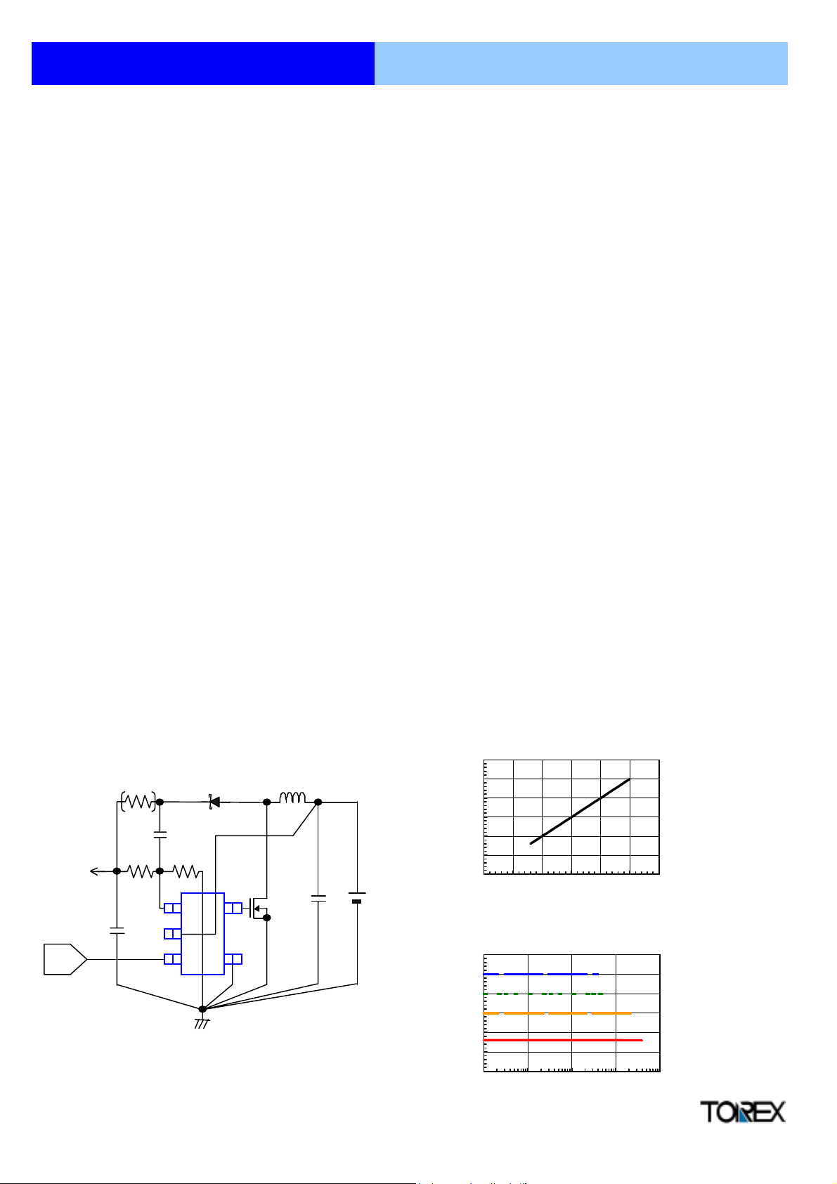
Typical Application Circui
RSENSE : 100m Ω
for Ceramic CL
*
VOUT = 8V~25V
I
OUT = 30mA
Ceramic CL :
0.8V~2.5V
D/A converter
* R
SENSE is of no use in light load (uncontinuous mode)
RFB1 :
270k Ω
10µF
CE/Vre
applications such as a small LCD, even using ceramic capacitor.
SD : MA737
CFB : 27pF
RFB2 :
30k Ω
15
2
3
4
L : 10µH
Nch Powe
MOS FET
2SK2159
CIN
VIN = 3.3V
Input Voltage Range: 0.9V ~ 10.0V
Power Supply Voltage Range: 1.8V ~ 10.0V and more than Vref+0.7V
VREF Input Range: 0.8V ~ 2.5V (±2.0%)
Output Voltage: Vref x external split resistor ratio
V
OUT=Vref x (RFB1+RFB2)/RFB2
Oscillation Frequency: 300kHz, 100kHz ±15%
Output Current: more than 30mA
(V
IN=3.3V, VOUT=20V, when peripheral
components are used as in the circuits
below .)
Controls: PWM (XC9106)
PWM/PFM auto-switching (XC9107)
High Efficiency: 85% (TYP.)
Stand-by Current: ISTB=1.0µA (MAX.)
Load Capacitors: Low ESR capacitors compatible
Packages: SOT-25, USP-6B
Electrical Characteristic
XC9107D003MR
DD=VIN=3.3V, IOUT=30mA
30
25
20
(V)
15
OUT
V
10
5
0
0.0 0.5 1.0 1.5 2.0 2.5 3.0
XC9107D003MR
30
25
20
(V)
15
OUT
V
10
5
0
0.1 1 10 100 1000
V
Vref (V)
I
OUT (mA)
1
Circuit as left
Circuit as left
V
DD=VIN=3.3V
2.5V
2.0V
1.5V
Vref=0.8V
t
s
PWM Control, PWM/PFM Switching Control,
r
r
f
XC9106 / 07 Series
Preliminary
Step-up DC/DC Converters
Externally Applied Reference Voltage (Vref)
Pin Configuration Pin Assignmen
12
SOT-25
(TOP VIEW)
PIN NUMBER
SOT-25 USP-6B
45
1
2
3
3
6
5
4
USP-6B
(TOP VIEW)
1
2
34
4
5
-5
PIN
NAME
FB
6
V
2
3
1
DD
CE/
Vref
NC No Connection
Output Resistor Connection
Serves as both Chip Enable pin and
Reference Voltage Apply pin.
External Transistor ConnectionEXT
FUNCTION
Supply Voltage
GroundGND
Ordering Information
XC9106D12345
XC9106 Series: PWM Control (Ordering information is the same as XC9106 Series)
12
3
4
5
Reference Voltage (apply external)
Fixed : 00
Oscillation Frequency: 300kHz
3
1
Package: SOT-25 (1 reel = 3000 pcs.)
M
D
Embossed Tape: Standard Feed
R
L
USP-6B (1 reel = 3000 pcs.)
Reverse Feed
100kHz
XC9107D12345
XC9107 Series: PWM/PFM automatic switching control
Block Diagram
Current
CE
Ripple Detect
and FB
Error Amp.
PWM/PFM
Controlle
FB
Vref with
Soft Start,
CE / Vre
Absolute Maximum Rating
PARAMETER
V
DD pin Voltage
FB pin Voltage
CE / Vref pin Voltage
EXT pin Voltage
EXT pin Current
Power Dissipation
Operating Ambient Temperature
Storage Temperature
Compensation
SYMBOL
V
DD
FB
V
CE / Vref
VEXT
IEXT/
SOT-25
Pd
USP-6B
Topr
Tstg
Phase
PWM
Comparato
Ramp Wave
Generator,
OSC
FB, CE : CMOS INPUT
EXT : CMOS OUTPUT
RATINGS UNITS
-0.3 ~ 12.0
-0.3 ~ 12.0
-0.3 ~ 12.0 V
-0.3 ~ V
DD + 0.3
±100
150
100
-40 ~ +85
-55 ~ +125
Buffer,
Driver
2
Ta = 25OC
V
V
V
mA
mW
O
C
O
C
VDD
EXT
GND
PWM Control, PWM/PFM Switching Control,
XC9106 / 07 Series
Preliminary
Step-up DC/DC Converters
Externally Applied Reference Voltage (Vref)
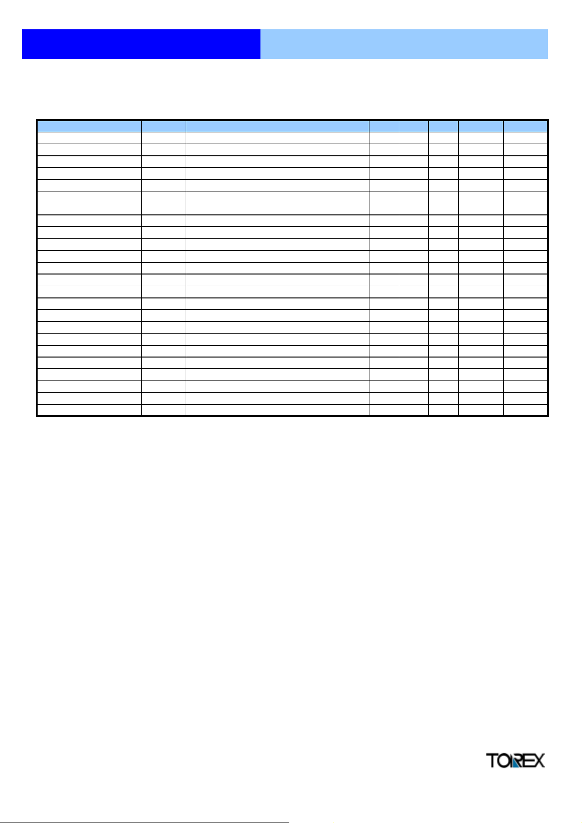
Electrical Characteristics
XC9106D001MR, XC9107D001MR (FOSC=100 (kHz) Ta=25OC
PARAMETER
Output Voltage
Reference Voltage Range
FB Control Voltage
Power Supply Voltage Range
*1
Operation Start Voltage
*1
Oscillation Start Voltage VST2
Operation Holding Voltage
Supply Current 1
Supply Current 2
Stand-by Current
Oscillation Frequency
Maximum Duty Ratio
PFM Duty Ratio
Efficiency
CE "High" Voltage
CE "Low" Voltage
EXT "High" ON Resistance
EXT "Low" ON Resistance
CE "High" Current
CE "Low" Current
FB "High" Current
FB "Low" Current
Test Conditions: Unless otherwise stated, CL: ceramic, recommended MOS FET should be connected.
DD = (V) D Vref = (V) , RFB1, 2 x 10
V
V
IN = (V) D IOUT = (mA)
SYMBOL
OUT
MAXDTY
PFMDTY
3.30
3.30
V
Vref
V
VDD
V
VHLD
IDD1
IDD2
STB
I
FOSC
T
V
V
REXTH
EXTL
R
ICEH
CEL
I
FBH
I
Vref = 0.9V
FB
Vref = 0.9V
VDD as shown right or (Vref applied voltage + 0.7V)
ST1 Recommended Circuit using 2SD1628, IOUT=1.0mA
No external connections
CE/Vref=0.9V, Voltage applied, FB=0V
Recommended Circuit using 2SD1628, IOUT=1.0mA
Same as VST2, VDD=3.300V
Same as I
Same as IDD1, CE/Vref=0V
Same as IDD1
Same as I
No Load (XC9106 series)
Recommended Circuit using XP161A1355EFFI %
SS
CEH Same as IDD1
CEL Same as IDD1
Same as IDD1, VEXT=VOUT-0.4V
Same as I
Same as IDD2, CE=2.5V
Same as IDD2, CE=0V
Same as I
Same as I
CONDITIONS
DD1, FB=1.2V
DD1
DD1, VEXT=0.4V
DD2, CE=VDD
DD2, CE=0VIFBL
0.09
50
MIN. TYP. MAX.
8.820 9.000 9.180
0.8 2.5
0.882 0.900 0.918
1.8
5.0 10.0 20.0
0.65
0.0
10.0
0.9
0.8
0.7
29 41
14 19
1.0
85 100 115
75 81 87
20 28 36
85
0.20
16 24
2.5
-0.1
0.1
-0.1
UNITS
V
V
V 4
V -
V 3
V
V
µA
µA
µA
KHz
%
%
V
Ω24 36
µA
µA
µA
µA
Circuit
1
-
4
3
4
4
5
4
4
1
1
1Soft-start Time Vref=0.9V mS
5
5V
4
4Ω
5
5
5
5
Notes
Although the IC starts step-up operations from a V
*1
V
DD ≥ 1.8V or (Vref applied voltage + 0.7V). Therefore, a VDD of more than 1.8V or (Vref applied voltage + 0.7V) is recommended when
DD is supplied from VIN or other power sources.
V
DD of 0.8V, the output voltage and oscillation frequency are stabilized at
3
 Loading...