

XC9101 Series
ETR0403_004a
PWM Controlled Step-Up DC/DC Controller
■GENERAL DESCRIPTION
The XC9101 series are step-up multiple current and voltage feedback DC/DC controller ICs. Current sense, clock
frequencies and amp feedback gain can all be externally regulated.
A stable power supply is possible with output currents of up to 1.5A.
With output voltage fixed internally, V
For output voltages outside this range, we recommend the FB version, which has a 0.9V internal reference voltage. Using this
version, the required output voltage can be set using 2 external resistors.
Switching frequency can also be set externally within a range of 100 ~ 600 kHz and therefore a frequency suited to your
particular application can be selected.
With the current sense function, peak currents (which flow through the driver transistor and the coil) can be controlled.
Soft-start time can be adjusted using external resistor and capacitor.
During shutdown (CE pin=L), consumption current can be reduced to as little as 0.5μA (TYP.) or less.
■APPLICATIONS
●Mobile, Cordless phones
●Palm top computers, PDAs
●Portable games
●Cameras, Digital cameras
●Note book PCs11
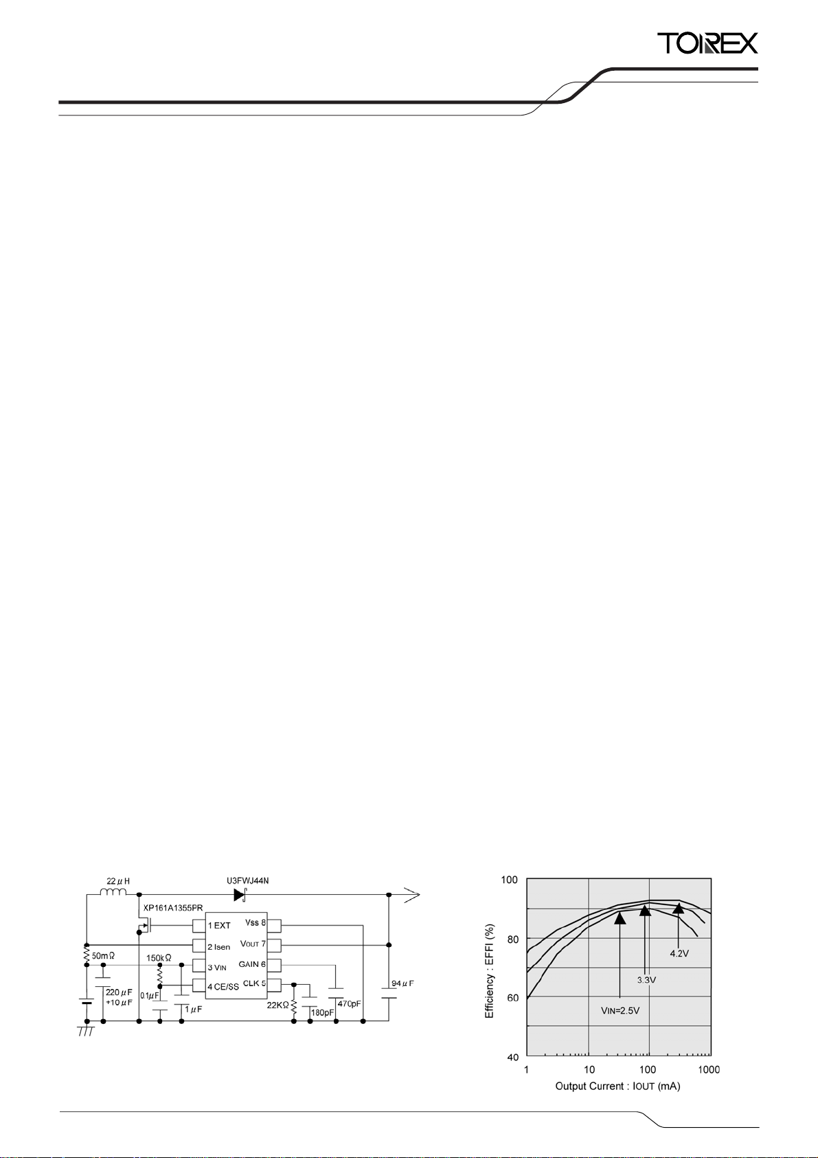
■TYPICAL APPLICATION CIRCUIT
OUT is selectable in 0.1V increments within a 2.5V ~ 16.0V range (±2.5%).
■FEATURES
Stable Operations via Current & Voltage
Multiple Feedback
Unlimited Options for Peripheral Selection
Current Protection Circuit
Ceramic Capacitor Compatible
Input Voltage Range : 2.5V ~ 20V
Output Voltage Range : 2.5V ~ 16V
(Fixed Voltage Type)
: 30V + (Adjustable Type)
Oscillation Frequency Range
: 100 kHz ~ 600kHz
Output Current : Up to 1.5A
Operating Ambient Temperature
Packages : MSOP-8A, SOP-8
:-40℃~+85℃
■TYPICAL PERFORMANCE
CHARACTERISTICS
VOUT=5.0V, f
=180 kHz
OSC
1/22
XC9101 Series
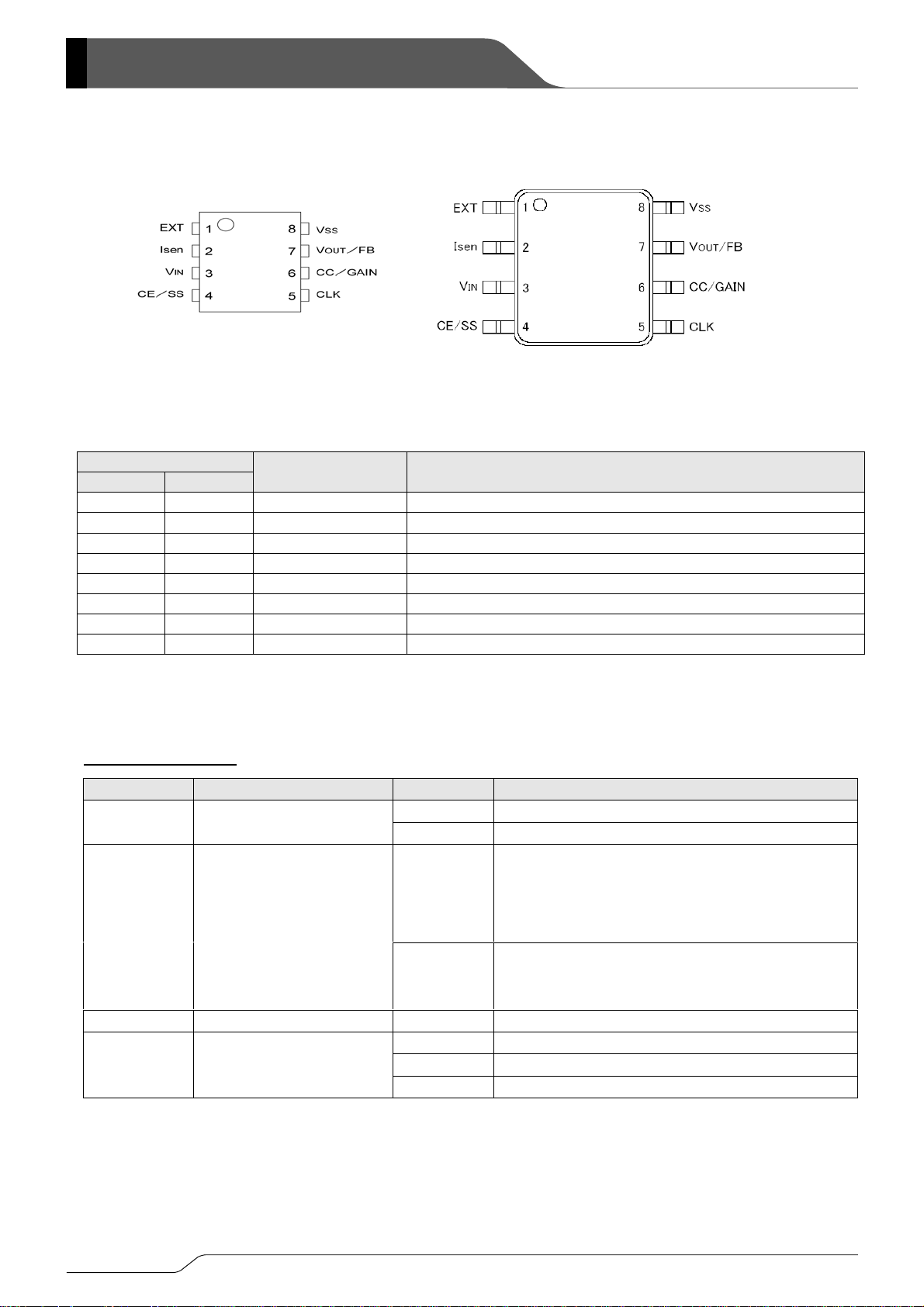
■PIN CONFIGURATION
■PIN ASSIGNMENT
PIN NUMBER
MSOP-8A SOP-8
1 1 EXT Driver
2 2 Isen Current Sense
3 3 VIN Power Input
4 4 CE/SS CE/Soft Start
5 5 CLK Clock Input
6 6 CC/GAIN Phase Compensation
7 7 VOUT/FB Voltage Sense
8 8 VSS Ground
■PRODUCT CLASSIFICATION
●Ordering Information
XC9101①②③④⑤⑥-⑦
MSOP-8A
(TOP VIEW)
(*1)
PIN NAME FUNCTION
SOP-8
(TOP VIEW)
DESIGNATOR ITEM SYMBOL DESCRIPTION
①
Type of DC/DC Controllers
C VOUT (Fixed voltage type), Soft-start externally set-up
D FB (Voltage adjustable), Soft-start externally set-up
e.g. VOUT=2.5V→②=2, ③=5
FB products→②=0, ③=9 fixed
25 ~ H0
Voltages above 10V
→10=A, 11=B, 12=C, 13=D, 14=E, 15=F, 16=H
② ③
④
Output Voltage
09
e.g. V
OUT=13.5V → ②=D, ③=5
FB products→②=0, ③=9 fixed
Oscillation Frequency A Frequency adjustable
KR MSOP-8A (1,000/Reel)
⑤⑥-⑦
Packages (Order Unit)
KR-G MSOP-8A (1,000/Reel)
SR SOP-8 (1,000/Reel)
(*1)
The “-G” suffix denotes Halogen and Antimony free as well as being fully RoHS compliant.
The standard output voltages of the XC9101C series are 2.5V, 3.3V, and 5.0V.
Voltages other than those listed are semi-custom.
2/22
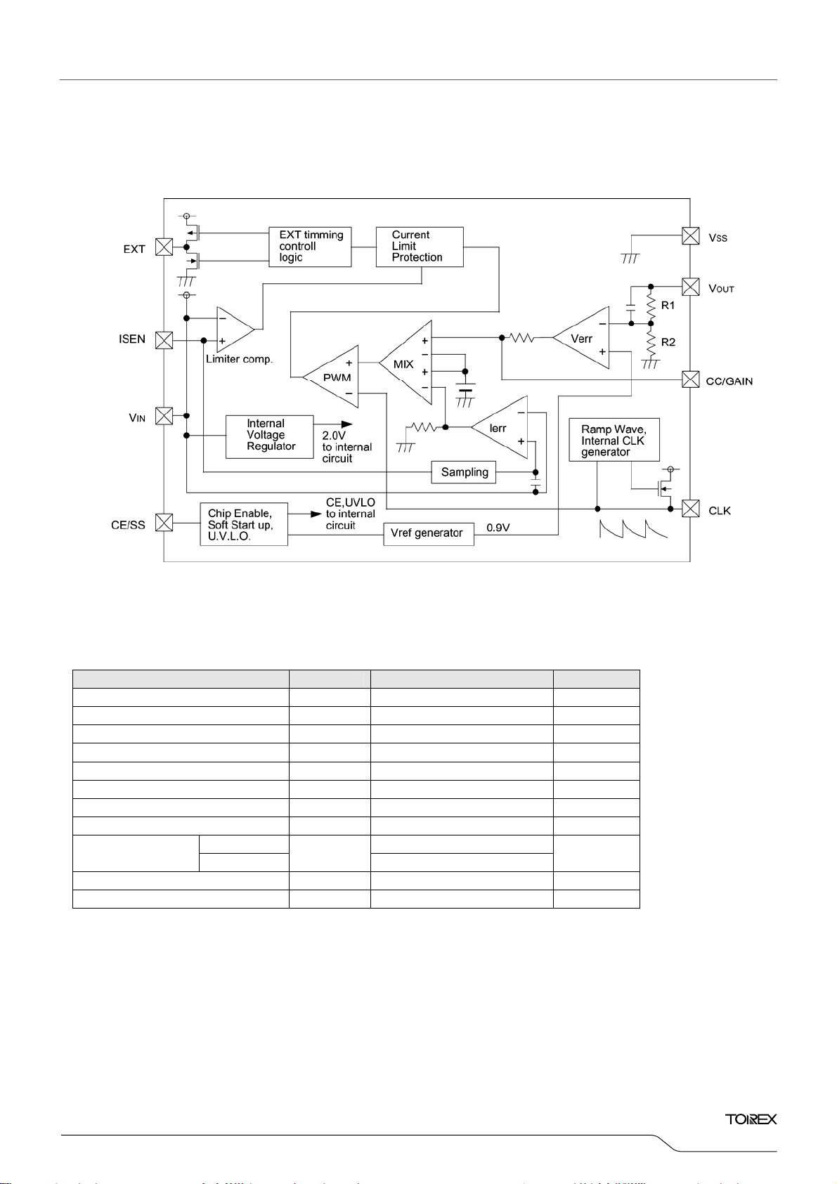
■BLOCK DIAGRAM
■ABSOLUTE MAXIMUM RATINGS
PAR AMETER SYMBOL RATINGS UNITS
EXT Pin Voltage VEXT
Isen Pin Voltage VIsen
VIN Pin Voltage VIN
CE/SS Pin Voltage VCE
CLK Pin Voltage VCLK
CC/GAIN Pin Voltage VCC
VOUT/FB Pin Voltage VOUT/FB
EXT Pin Current IEXT
Power Dissipation
MSOP-8A 150
SOP-8
Pd
Operating Ambient Temperature Topr
Storage Temperature Tstg
-0.3~V
IN+0.3
-0.3~+22
-0.3~+22
-0.3~+22
-0.3~V
-0.3~V
IN+0.3
IN+0.3
-0.3~+22
±100
300
-40~+85 ℃
-55~+125 ℃
Ta = 2 5 ℃
V
V
V
V
V
V
V
mA
mW
XC9101
Series
3/22
XC9101 Series
■ELECTRICAL CHARACTERISTICS
XC9101C33AKR
PAR AMETER SYMBOL CONDITIONS MIN. TYP. MAX. UNITS CIRCUITS
Output Voltage VOUT IOUT=300mA 3.218 3.300 3.382 V
Maximum
Operating Voltage
Minimum
Operating Voltage
Supply Current 1 IDD1
Supply Current 2 IDD2
Stand-by Current I
CLK
Oscillation Frequency
Frequency
Line Regulation
Frequency
Temperature Fluctuation
Maximum Duty Cycle D
Minimum Duty Cycle D
Current Limit Voltage ILIM
ISEN Current IISEN VIN=2.5V, ISEN=2.5V 4.5 7 13
VINmax 20
VINmin
VIN=2.5V, VOUT=CE=
Setting Output Voltage×0.95V
VIN=2.5V, CE=VIN
OUT=Setting Output Voltage×1.05V
V
VIN=2.5V, CE=VOUT=VSS 0.5 2.0
STB
f
RT=10.0kΩ, CT=220pF 280 330 380 kHz
OSC
Δf
ΔVIN・f
Δf
ΔTopr・f
OSC
OSC
MAX
MIN
VIN=2.5V ~ 20V
OSC
VIN=2.5V
Topr=-40 ~ +85℃
OSC
VOUT=Set Voltage×0.95V 79 85 89 %
VOUT=Set Voltage×1.05V
IN pin voltage-ISEN pin voltage
V
- -
-
-
- ±5 -
- ±5 -
- -
90 150 220 mV
- -
2.5 V
150 255
90 176
0 %
V
μA ②
μA ②
μA ②
%
%
μA ⑥
Ta =2 5℃
①
①
①
③
③
③
④
④
⑥
CE "High" Current ICEH CE=VIN=2.5V, VOUT=0V -0.1 0 0.1
CE "Low" Current ICEL CE=0V, VIN=2.5V, VOUT=0V -0.1 0 0.1
CE "High" Voltage VCEH
CE "Low" Voltage VCEL
EXT "High" ON
Resistance
EXT "Low" ON
Resistance
Efficiency
(*1)
EFFI
R
R
EXTH
EXTL
Soft-Start Time tSS
CC/GAIN Pin
Output Impedance
Unless otherwise stated, VIN = 2.5V
NOTE:
*1: EFFI = {[(output voltage) × (output current)] ÷ [(input voltage) × (input current)]} × 100
*2: The capacity range of the capacitor used to set the external CLK frequency is 150 ~ 220pF
RCCGAIN
CLK Oscillation Starts,
V
OUT=0V, CE: Voltage applied
CLK Oscillation Stops,
V
OUT=0V, CE: Voltage applied
IN-0.4V, CE=VIN=2.5V
EXT=V
OUT=Setting voltage×0.95V
V
EXT=0.4V, CE=V
V
OUT=Setting voltage×1.05
IN=2.5V
Connect CSS and RSS,
CE : 0V→2.5V
0.6
- -
-
-
-
- -
0.2 V
31 58
27 45
88
-
5 10 20 ms
-
400
- kΩ ⑦
μA ⑤
μA ⑤
V
Ω ④
Ω ④
%
⑤
⑤
①
①
4/22
XC9101
Series
■ELECTRICAL CHARACTERISTICS (Continued)
XC9101C50AKR
PAR AMETER SYMBOL CONDITIONS MIN. TYP. MAX. UNITS CIRCUITS
Output Voltage VOUT IOUT=300mA 4.875 5.000 5.125 V
Maximum
Operating Voltage
Minimum
Operating Voltage
Supply Current 1 IDD1
Supply Current 2 IDD2
Stand-by Current I
CLK
Oscillation Frequency
Frequency
Line Regulation
Frequency
Temperature Fluctuation
Maximum Duty Cycle D
Minimum Duty Cycle D
Current Limit Voltage ILIM
ISEN Current IISEN VIN=3.0V, ISEN=3.0V 4.5 7 13
CE "High" Current ICEH CE=VIN=3.0V, VOUT=0V -0.1 0 0.1
CE "Low" Current ICEL CE=0V, VIN=3.0V, VOUT=0V -0.1 0 0.1
CE "High" Voltage VCEH
CE "Low" Voltage VCEL
EXT "High"
ON Resistance
EXT "Low"
ON Resistance
Efficiency
(*1)
EFFI
Soft-Start Time tSS
CC/GAIN Pin
Output Impedance
NOTE: Unless otherwise stated, VIN = 3.0V.
*1: EFFI = {[(output voltage) × (output current)] ÷ [(input voltage) × (input current)]} × 100
*2: The capacity range of the capacitor used to set the external CLK frequency is 150 ~ 220pF
VINMAX 20
VINMIN
VIN=3.0V, VOUT=CE=
Setting Output Voltage×0.95V
IN=3.0V, CE=VIN
V
V
OUT=Setting Output Voltage×1.05V
VIN=3.0V, CE=VOUT=VSS
STB
f
RT=10.0kΩ, CT=220pF 280 330 380 kHz
OSC
Δf
ΔVIN・f
Δf
ΔTopr・f
OSC
OSC
OSC
OSC
VOUT=Setting Voltage×0.95V 79 85 89 %
MAX
VOUT=Setting Voltage×1.05V
MIN
IN=2.5V~20V - ±5 -
V
VIN=2.5V
Topr=-40~+85℃
IN pin voltage-ISEN pin voltage
V
CLK Oscillation Starts,
V
OUT=0V, CE: Voltage applied
CLK Oscillation Stops,
V
OUT=0V, CE: Voltage applied
IN-0.4V, CE=VIN=3.0V
REXTH
REXTL
EXT=V
V
OUT=Setting voltage×0.95V
EXT=0.4V, CE=VIN=3.0V
V
OUT=Setting voltage×1.05V
- -
-
-
-
- ±5 -
- -
90 150 220 mV
0.6
- -
-
-
-
CCGAIN
R
Connect C
CE: 0V→3.0V
SS and RSS,
-
-
- -
160 270
90 176
0.5 2.0
- -
27 51
25 37
87
5
400
V
2.5 V
μA ②
μA ②
μA ②
%
%
0 %
μA ⑥
μA ⑤
μA ⑤
V
0.2 V
Ω ④
Ω ④
-
-
%
ms
- kΩ ⑦
Ta =2 5℃
①
①
①
③
③
③
④
④
⑥
⑤
⑤
①
①
5/22
XC9101 Series
■ELECTRICAL CHARACTERISTICS (Continued)
XC9101D09AKR
PAR AMETER SYMBOL CONDITIONS MIN. TYP. MAX. UNITS CIRCUITS
Output Voltage VOUT IOUT=300mA 0.8775 0.9 0.9225 V
Maximum
Operating Voltage
Minimum
Operating Voltage
Supply Current 1 IDD1 VIN=2.5V, VIN=CE, FB=0.9×0.95V
Supply Current 2 IDD2
Stand-by Current I
CLK
Oscillation Frequency
Frequency
Line Regulation
Frequency
Temperature Fluctuation
Maximum Duty Cycle D
Minimum Duty Cycle D
Current Limiter Voltage ILIM
ISEN Current IISEN VIN=2.5V, ISEN=2.5V 4.5 7 13
CE "High" Current ICEH CE=VIN=2.5V, FB=0V -0.1 0 0.1
CE "Low" Current ICEL CE=0V, VIN=2.5V, FB=0V -0.1 0 0.1
CE "High" Voltage VCEH
CE "Low" Voltage VCEL
EXT "High"
ON Resistance
EXT "Low"
ON Resistance
Efficiency
(*1)
EFFI
Soft-Start Time tSS
CC/GAIN Pin
Output Impedance
NOTE: Unless otherwise stated, VIN = 2.5V
External Components: R
*1: EFFI = {[(output voltage) × (output current)] ÷ [(input voltage) × (input current)]} × 100
*2: The capacity range of the capacitor used to set the external CLK frequency is 150 ~ 220pF.
VINMAX 20
VINMIN
- -
-
VIN=2.5V, CE=VIN,
V
OUT=0.9×1.05V
VIN=2.5V, CE=FB=VSS
STB
RT=10.0kΩ, CT=220pF 280 330 380 kHz
f
OSC
Δf
ΔV
Δf
ΔTopr・f
OSC
IN・f
OSC
MAX
MIN
V
IN=2.5V~20V - ±5 -
OSC
VIN=2.5V
Topr=-40~+85℃
OSC
VOUT=0.9×0.95V 79 85 89 %
VOUT=0.9×1.05V 0 %
IN pin voltage-ISEN pin voltage
V
-
-
- ±5 -
90 150 220 mV
- -
2.5 V
150 255
90 176
0.5 2.0
μA ②
μA ②
μA ②
μA ⑥
μA ⑤
μA ⑤
CLK Oscillation Start,
FB=0V, CE: Voltage applied
CLK Oscillation Stop,
FB=0V, CE: Voltage applied
IN-0.4V, CE=VIN
REXTH
R
EXTL
EXT=V
OUT=Setting voltage×0.95V
V
EXT=0.4V, CE=V
V
OUT=Setting voltage×1.05V
Connect C
IN
SS and RSS,
CE : 0V→2.5V
CCGAIN
R
FB1=200kΩ, RFB2=100kΩ, CFB=82pF
0.6
- -
-
-
-
- -
0.2 V
31 58
27 45
88
-
5 10 20 ms
-
400
- kΩ ⑦
Ta =2 5℃
①
V
①
①
③
%
%
③
③
④
④
⑥
V
⑤
⑤
Ω ④
Ω ④
%
①
①
6/22
XC9101
■TYPICAL APPLICATION CIRCUITS
XC9101C33AKR
NMOS : XP161A1355PR
Coil : 22μH (CR105 SUMIDA)
Resistor : 20mΩ for I
Capacitors : 180pF (ceramic) for CLK, 470pF (ceramic) for CC/GAIN, 0.1μF (ceramic) for SS,1μF (ceramic) for Bypass
SD : U3FWJ44N (TOSHIBA)
XC9101C50AKR
NMOS : XP161A1355PR
Coil : 22μH (CR105 SUMIDA)
Resistor : 20mΩ for ISEN (NPR1 KOA), 33kΩ(trimmer) for CLK, 100kΩ for SS
Capacitors : 180pF (ceramic) for CLK, 470pF (ceramic) for CC/GAIN, 0.1μF (ceramic) for SS,1μF (ceramic) for Bypass
SD : U3FWJ44N (TOSHIBA)
47μF (OS)+220μF (any) for CL, 220μF (any) for C
47μF (OS)+220μF (any) for CL, 220μF(any) for C
SEN (NPR1 KOA), 33kΩ(trimmer) for CLK, 100kΩ for SS
IN
IN
Series
7/22

XC9101 Series
■TYPICAL APPLICATION CIRCUITS (Continued)
XC9101D09AKR
NMOS : XP161A11A1PR
Coil : 22μH (CDRH127 SUMIDA)
Resistor : 10mΩ for I
Capacitors : 180pF (ceramic) for CLK, 470pF (ceramic) for CC/GAIN, 0.1μF (ceramic) for SS, 1μF (ceramic) for Bypass
SD : U5FWJ44N (TOSHIBA)
V
OUT : 16V
RFB1 : 560kΩ
R
FB2 : 33kΩ
FB : 27pF
C
V
OUT : 20V
RFB1 : 470kΩ
R
FB2 : 22kΩ
FB : 33pF
C
47μF (OS)+220μF (any) for CL, 220μF (any) for C
SEN (NPR1 KOA), 33kΩ(trimmer) for CLK, 150kΩ for SS
IN
8/22

XC9101
■OPERATIONAL EXPLANATION
Step-up DC/DC converter controllers of the XC9101 series carry out pulse width modulation (PWM) according to the
multiple feedback signals of the output voltage and coil current. The internal circuits consist of different blocks that
operate at VIN or the stabilized power (2.0 V) of the internal regulator. The fixed output voltage of the C type and the FB
pin voltage (Vref = 0.9 V) of type D controller have been adjusted and set by laser-trimming.
<Clock>
With regard to clock pulses, a capacitor and resistor connected to the CLK pin generate ramp waveforms whose top and
bottom are 0.7V and 0.15V, respectively. The frequency can be set within a range of 100kHz to 600kHz externally (refer to
the "Functional Settings" section for further information). The clock pulses are processed to generate a signal used for
synchronizing internal sequence circuits.
<Verr amplifier>
The Verr amplifier is designed to monitor the output voltage. A fraction of the voltage applied to internal resistors R1, R2 in
the case of a type C controller, and the voltage at the FB pin in the case of a type D controller, are fed back and compared
with the reference voltage. In response to feedback of a voltage lower than the reference voltage, the output voltage of
the Verr amplifier increases. The output of the Verr amplifier enters the mixer via resistor (R
pulse width control signal during PWM operations. By connecting an external capacitor and resistor through the CE/GAIN
pin, it is possible to set the gain and frequency characteristics of Verr amplifier signals (refer to the "Functional Settings"
section for further information).
<Ierr amplifier>
The Ierr amplifier monitors the coil current. The potential difference between the V
switching operation. Then the potential difference is amplified or held, as necessary, and input to the mixer. The Ierr
amplifier outputs a signal ensuring that the greater the potential difference between the VIN and ISEN pins, the smaller the
switching current. The gain and frequency characteristics of this amplifier are fixed internally.
<Mixer and PWM>
The mixer modulates the signal sent from Verr by the signal from Ierr. The modulated signal enters the PWM comparator
for comparison with the sawtooth pulses generated at the CLK pin. If the signal is greater than the sawtooth waveforms, a
signal is sent to the output circuit to turn on the external switch.
<Current Limiter>
The current flowing through the coil is monitored by the limiter comparator via the V
comparator outputs a signal when the potential difference between the V
This signal is converted to a logic signal and handled as a DFF reset signal for the internal limiter circuit. When a reset
signal is input, a signal is output immediately at the EXT pin to turn off the MOS switch. When the limiter comparator
sends a signal to enable data acceptance, a signal to turn on the MOS switch is output at the next clock pulse. If at this
time the potential difference between the V
DFF operates in synchronization with the clock signal of the CLK pin.
<Soft Start>
The soft start function is made available by attaching a capacitor and resistor to the CE/SS pin. The Vref voltage applied to
the Verr amplifier is restricted by the start-up voltage of the CE/SS pin. This ensures that the Verr amplifier operates with its
two inputs in balance, thereby preventing the ON-TIME signal from becoming stronger than necessary. Consequently, soft
start time needs to be set sufficiently longer than the time set to CLK. The start-up time of the CE/SS pin equals the time set
for soft start (refer to the "Functional Settings" section for further information). The soft start function operates when the
voltage at the CE/SS pin is between 0V to 1.55V. If the voltage at the CE/SS pin doesn't start from 0V but from a mid level
voltage when the power is switched on, the soft start function become ineffective and large in-rush currents and ripple voltages
may happen to create.
PWM/PFM switching signal
CLK synchronous signal
IN and ISEN pins is large, operation is repeated to turn off the MOS switch again.
Limiter signal
/RESET
D
CLK
Q
IN and ISEN pins reaches about 150 mV or more.
Output signal to EXT pin
PWM/PFM switching signal
Verr). This signal works as a
IN and Isen pins is sampled at each
IN and ISEN pins. The limiter
Series
9/22

)
XC9101 Series
■OPERATIONAL EXPLANATION (Continued
●Functional Settings
1. Soft Start
CE and soft start (SS) functions are commonly assigned to the CE/SS pin. The soft start function is effective until the
voltage at the CE pin reaches approximately 1.55 V rising from 0 V. Soft start time is approximated by the equation below
according to values of Vcont, RSS, and CSS
Example: When C
T = -0.1 x 10
Set the soft start time to a value sufficiently longer than the period of a clock pulse.
> Circuit example 1: N-ch open drain
> Circuit example 2: CMOS logic (low supply current)
T = - CSS × RSS × ln ((Vcont - 1.55) / Vcont)
-6
× 470 x 103 × ln ((5 - 1.55) / 5) = 17.44 ms.
.
SS = 0.1 μF, R SS = 470 kΩ, and Vcont = 5 V,
CE/SS pin
Rss
Vcont Css
ON/OFF signal
Vcont
ON/OFF signal
Css
Rss
CE,
UVLO
Vcont
Rss
Css
Vref
circuit
CE/SS pin
CE/SS pin
To Verr amplifier
> Circuit example 3: CMOS logic (low supply current), quick off
Vcont
Rss
ON/OFF signal
10/22
CE/SS pin
Css

XC9101
■OPERATIONAL EXPLANATION (Continued)
●Functional Settings (Continued)
2. Oscillation Frequency
The oscillation frequency of the internal clock generator is approximated by the following equation according to the values
of the capacitor and resistor attached to the CLK pin. To stabilize the IC's operation, set the oscillation frequency within a
range of 100kHz to 600kHz. Select a value for Cclk within a range of 150pF to 220pF and fix the frequency based on the
value for Rclk.
×
Example: When Cclk = 220 pF and Rclk = 10 kΩ, f = 1 / (-220 x 10
3. Gain and Frequency Characteristics of the Verr Amplifier
The gain at output and frequency characteristics of the Verr amplifier are adjusted by the values of the capacitor and
resistor attached to the CC/GAIN pin. It is generally recommended to attach a CC of 220 to 1,000pF without R
greater the CC value, the more stable the phase and the slower the transient response. When using the IC with RGAIN
connected, it should be noted that if the RGAIN resistance value is too high, abnormal oscillation may occur during transient
response time. The size of R
4. Current Limit
The current limit value is approximated by the following equation according to resistor R
SEN pins. Double function, current FB input and current limiting, is assigned to the ISEN pin. The current limiting value is
I
approximated by the following equation according to the value for R
Example: When RSEN = 100 mΩ, I
The inside error amplifier sends feedback signal when the voltage occurs at R
current in order to phase compensate. The more the R
bigger, and it could lead to an intermittent oscillation. Please be careful if there is a problem with the application. Under
the regular operation, a voltage created by a peak coil current at the R
voltage 90 mV (MIN). For more details, please refer the notes on the external components.
f = 1/(-Cclk
I
Lpeak_limit
Rclk × ln0.26)
Rclk
GAIN should be carefully evaluated before connection.
CC
= 0.15/R
SEN
Rsen
CLK pin
CC/GAIN pin
RGAIN
Lpeak_limit
Isen pin
Cclk
RVerr
= 0.15/0.1 = 1.5 A
IN
pin
V
Comparator with
150mV offset
-12
×
CLK Generator
Verr
SEN value becomes larger, the more the error signal becomes
V
Vref
SEN.
SEN
3
10 x 10
OUT
×
ln(0.26)) = 337.43 kHz.
/FB
SEN inserted between the VIN and
Limiter signal
SEN resistor because of the flow of coil
GAIN. The
resistor should be set lower than the current limit
Series
11/22

XC9101 Series
■OPERATIONAL EXPLANATION (Continued)
●Functional Settings (Continued)
5. FB Voltage and C
With regard to the XC9101D series, the output voltage is set by attaching externally divided resistors. The output voltage
is determined by the equation shown below according to the values of R
FB2 should be 1 MΩ or less.
R
The value of C
FB1 and fzfb. The value of fzfb should be 10 kHz, as a general rule.
R
Example: When R
■NOTES ON USE
●Application Notes
1. The XC9101 series are designed for use with an output ceramic capacitor. If, however, the potential difference
between input and output is too large, a ceramic capacitor may fail to absorb the resulting high switching energy and
oscillation could occur on the output side. If the input-output potential difference is large, connect an electrolytic
capacitor in parallel to compensate for insufficient capacitance.
2. The EXT pin of the XC9101 series is designed to minimize the through current that occurs in the internal circuitry.
However, the gate drive of external NMOS has a low impedance for the sake of speed. Therefore, if the input voltage is
high and the bypass capacitor is attached away from the IC, the charge/discharge current to the external NMOS may
lead to unstable operations due to switching operation of the EXT pin.
As a solution to this problem, place the bypass capacitor as close to the IC as possible, so that voltage variations at the
V
of ohms between the EXT pin and NMOS gate. Remember that the insertion of a resistor slows down the switching
speed and may result in reduced efficiency.
3. A NPN transistor can be used in place of NMOS. If using a NPN transistor, insert a resistor (R
between the EXT pin and the base of the NPN transistor in order to limit the base current without slowing the switching
speed. Adjust R
capacitor for C
4. Although the C_CLK connection capacitance range is from 150 ~ 220pF, the most suitable value for maximum stability is
around 180pF.
OUT = 0.9
V
C
FB = 1/(2
FB = 1/(2
: C
IN and VSS pins caused by switching are minimized. If this is not effective, insert a resistor of several to several tens
FB
FB1 and RFB2. In general, the sum of RFB1 and
×
(RFB1 + RFB2)/ RFB2
FB (phase compensation capacitor) is approximated by the following equation according to the values of
× π ×
FB1 = 455 kΩ and RFB2 = 100 kΩ : VOUT = 0.9
× π ×
Output voltage
B in a range of 500Ω to 1 kΩ according to the load and h
B, complying with CB < 1/(2
RFB1 × fzfb)
455 k × 10 k) = 34.98 pF
Cfb
Rfb1
Rfb2
×π×
EXT pin
Rb
Cb
FB pin
RB ×F
×
0.9V
×
0.7), as a rule.
OSC
V
IN
(455 k + 100 k)/100 k = 4.995 V
Verr
Verr amplifier
B) and capacitor (CB)
of the transistor. Use a ceramic
FE
12/22

)
XC9101
■NOTES ON USE (Continued
●Instruction on Pattern Layout
① In order to stabilize VDD voltage level, we recommend that a by-pass capacitor (CDD) be connected as close as
possible to the VIN & VSS pins.
② In order to stabilize the GND voltage level which can fluctuate as a result of switching, we suggest that C_CLK, R_CLK
and C_GAIN GND is separated from Power GND and connected as close as possible to the V
capacitor, C
< XC9101D Series Pattern Layout Examples>
2 Layer Better Evaluation Board
RSEN
VIN
DD). Please use a multi layer board and check the wiring carefully.
CIN
L
N-MOS
1
2
3
R_SS
4 5
C_SS
SD
CDD
8
7
6
R_CLK
C_CLK
RFB1
C_GAIN
CFB
RFB2
Through Hole
1
2
3
4
8
7
6
5
R_CLK,C_CLK,C_GAIN,RFB2
GND
Through Hole
CL
VDD line
IC GND
Power GND
SS pin (by-pass
Series
13/22

)
XC9101 Series
■NOTES ON USE (Continued
●Instruction on Pattern Layout (Continued)
1 Layer Good Evaluation Board
●Notes
1. Ensure that the absolute maximum ratings of the external components and the XC9101 DC/DC IC itself are not exceeded.
2. We recommend that sufficient counter measures are put in place to eliminate the heat that may be generated by the external
3. Try to use a N-channel MOSFET with a small gate capacitance in order to avoid overly large output spike voltages that may
4. The performance of the XC9101 DC/DC converter is greatly influenced by not only its own characteristics, but also by those of
5. Wire external components as close to the IC as possible and use thick, short connecting wires to reduce wiring impedance.
6. Make sure that the GND wiring is as strong as possible as variations in ground potential caused by ground current at the time
RSEN
VIN
N-channel MOSFET as a result of switching losses.
occur (such spikes occur in proportion to gate capacitance).
the external components it is used with. We recommend that you refer to the specifications of each component to be used and
take sufficient care when selecting components.
In particular, minimize the distance between the by-pass capacitor and the IC.
of switching may result in unstable operation of the IC. Specifically, strengthen the ground wiring in the proximity of the V
pin.
CIN
L
N-MOS
1
2
3
R_SS
4
C_SS
SD
CDD
8
7
6
5
R_CLK
C_CLK
C_GAIN
RFB1
RFB2
CFB
CL
VDD line
IC GND
Power GND
SS
14/22

■TEST CIRCUITS
・Circuit ① (V
22μH
100mΩ
220μF
NMOS
R_SS
0.1μF
OUT Type)
1 EXT
2 Isen
3 V
4 CE/SS
1μF
SD
Vss 8
OUT
7
V
GAIN 6
IN
CLK 5
10KΩ
XC9101C33A R_SS:104kΩ C-SS:0.1μF
XC9101C50A R_SS:138kΩ C-SS:0.1μF
・Circuit ②
Vss 8
A
0.1μF
1 EXT
2 Isen
IN
3 V
4 CE/SS
OUT
V
/FB 7
GAIN 6
CLK 5
10KΩ
・Circuit ④
1 EXT
OSC
0.1μF
2 Isen
3 V
IN
4 CE/SS
V
OUT
GAIN 6
CLK 5
Vss 8
/FB 7
・Circuit ⑥
A
V
0.1μF
1 EXT
2 Isen
IN
3 V
4 CE/SS
V
OUT
GAIN 6
220pF
10KΩ
Vss 8
/FB 7
CLK 5
220pF
10KΩ
470pF
220pF
20μF
220pF
XC9101
Series
・Circuit ① (FB Type)
SD22μH
NMOS
1 EXT
Vss 8
2 Isen
100mΩ
220μF
R_SS
0.1μF
1μF
RL
V
IN
3 V
4 CE/SS
FB 7
GAIN 6
CLK 5
10KΩ
・Circuit ③
Vss 8
1 EXT
V
OUT
/FB 7
2 Isen
GAIN 6
IN
3 V
CLK 5
4 CE/SS
0.1μF
10KΩ
・Circuit ⑤
1 EXT
V
0.1μF
2 Isen
3 V
IN
4 CE/SS
A
・Circuit ⑦
1 EXT
Vss 8
V
OUT
/FB 7
2 Isen
GAIN 6
3 V
IN
CLK 5
4 CE/SS
0.1μF
V
OUT
GAIN 6
CLK 5
Vss 8
/FB 7
CFB
220pF
220pF
10KΩ
RFB2
470pF
1MΩ
RFB1
OSC
220pF
RL
V
20μF
V
V
15/22

XC9101 Series
■TYPICAL PERFORMANCE CHARACTERISTICS
XC9101D09AKR
(1) Output Voltage vs. Output Current
16/22

■TYPICAL PERFORMANCE CHARACTERISTICS(Continued)
XC9101D09AKR
(2) Efficiency vs. Output Current
V
V
XC9101
Series
17/22

XC9101 Series
■TYPICAL PERFORMANCE CHARACTERISTICS(Continued)
XC9101D09AKR
(3) Ripple Voltage vs. Output Current
Note : If the difference between the input and output voltage is large or small, switching ON/OFF time will be
18/22
shortened. As such, the external components used and their values (inductance value of the coil, resistor
connected to CLK, capacitor etc.) may have a critical influence on the actual operation of the IC.

■PACKAGING INFORMATION
●MSOP-8A
XC9101
Series
●SOP-8
19/22

XC9101 Series
■ MARKING RULE
● MSOP-8A
MSOP-8A
(TOP VIEW)
①Represents product series
MARK PRODUCT SERIES
4 XC9101xxxAKx
②Represents type of DC/DC controller
MARK TYPE PRODUCT SERIES
C VOUT, CE PIN XC9101CxxAKx
D FB, CE PIN XC9101D09AKx
③Represents integral number of output voltage, or FB type
MARK VOLTAGE (V) PRODUCT SERIES
2 2.x XC9101C2xAKx
3 3.x XC9101C3xAKx
4 4.x XC9101C4xAKx
5 5.x XC9101C5xAKx
6 6.x XC9101C6xAKx
7 7.x XC9101C7xAKx
8 8.x XC9101C8xAKx
9 9.x XC9101C9xAKx
0 FB products XC9101D09AKx
A 10.x XC9101CAxAKx
B 11.x XC9101CBxAKx
C 12.x XC9101CCxAKx
D 13.x XC9101CDxAKx
E 14.x XC9101CExAKx
F 15.x XC9101CFxAKx
H 16.x XC9101CHxAKx
④Represents decimal number of output voltage, FB products (ex.)
MARK VOLTAGE (V) PRODUCT SERIES
0 x.0 XC9101Cx0AKx
3 x.3 XC9101C3xAKx
9 FB products XC9101D09AKx
⑤Represents control type of oscillation frequency
MARK TYPE PRODUCT SERIES
A Adjustable Frequency XC9101xxxAKx
⑥Represents production lot number
0 to 9, A to Z repeated (G, I, J, O, Q, W excepted).
Note: No character inversion used.
20/22

■ MARKING RULE (Continued)
●SOP-8
①②Represents product series
① ②
0 1 XC9101xxxASx
③Represents type of DC/DC controller
MARK TYPE PRODUCT SERIES
C VOUT, CE pin XC9101CxxAKx
D FB, CE pin XC9101D09AKx
SOP-8
(TOP VIEW)
④Represents integral number of output voltage, or FB type
MARK
VOLTAGE
2 2.x XC9101C2xAKx A 10.x XC9101CAxAKx
3 3.x XC9101C3xAKx B 11.x XC9101CBxAKx
4 4.x XC9101C4xAKx C 12.x XC9101CCxAKx
5 5.x XC9101C5xAKx D 13.x XC9101CDxAKx
6 6.x XC9101C6xAKx E 14.x XC9101CExAKx
7 7.x XC9101C7xAKx F 15.x XC9101CFxAKx
8 8.x XC9101C8xAKx H 16.x XC9101CHxAKx
9 9.x XC9101C9xAKx
0 FB products XC9101C09AKx
⑤Represents decimal number of output voltage, FB type (ex.)
MARK VOLTAGE (V) PRODUCT SERIES
0 x.0 XC9101Cx0AKx
3 x.3 XC9101C3xAKx
9 FB products XC9101D09AKx
⑥Represents control type of oscillation frequency
MARK TYPE PRODUCT SERIES
A Variable by external C and R XC9101xxxAKx
⑦Represents the last digit of production year
⑧⑨Represents production lot number (ex.)
0 to 9, A to Z repeated (G, I, J, O, Q, W excluded).
Note: No character inversion used.
⑧ ⑨
0 3 03
0 A 1A
XC9101
Series
MARK PRODUCT SERIES
(V)
PRODUCT
SERIES
MARK
MARK YEAR
0 2000
6 2006
MARK
VOLTAGE
(V)
PRODUCTION LOT NUMBER
PRODUCT
SERIES
21/22

XC9101 Series
1. The products and product specifications contained herein are subject to change without
notice to improve performance characteristics. Consult us, or our representatives
before use, to confirm that the information in this catalog is up to date.
2. We assume no responsibility for any infringement of patents, patent rights, or other
rights arising from the use of any information and circuitry in this catalog.
3. Please ensure suitable shipping controls (including fail-safe designs and aging
protection) are in force for equipment employing products listed in this catalog.
4. The products in this catalog are not developed, designed, or approved for use with such
equipment whose failure of malfunction can be reasonably expected to directly
endanger the life of, or cause significant injury to, the user.
(e.g. Atomic energy; aerospace; transport; combustion and associated safety
equipment thereof.)
5. Please use the products listed in this catalog within the specified ranges.
Should you wish to use the products under conditions exceeding the specifications,
please consult us or our representatives.
6. We assume no responsibility for damage or loss due to abnormal use.
7. All rights reserved. No part of this catalog may be copied or reproduced without the
prior permission of Torex Semiconductor Ltd.
22/22
 Loading...