

■
■
■
■
A
■
XC74WL4066SR
ETR1326_001
CMOS Logic
GENERAL DESCRIPTIO N
XC74WL4066SR is dual analog switch manufactured using silicon gat e CMOS processes. The small supply current, which
is one of the features of the CMOS logic, gives way to high speed operations which enables LS-TTL.
With wave forming buffers connected internally, stabilized output can be achieved as the series offers high noise immunity.
As the series is integrated into a mini molded, MSOP-8B package, high density mounting is possible.
PPLICATIONS
●Palmtops
●Digital equipment
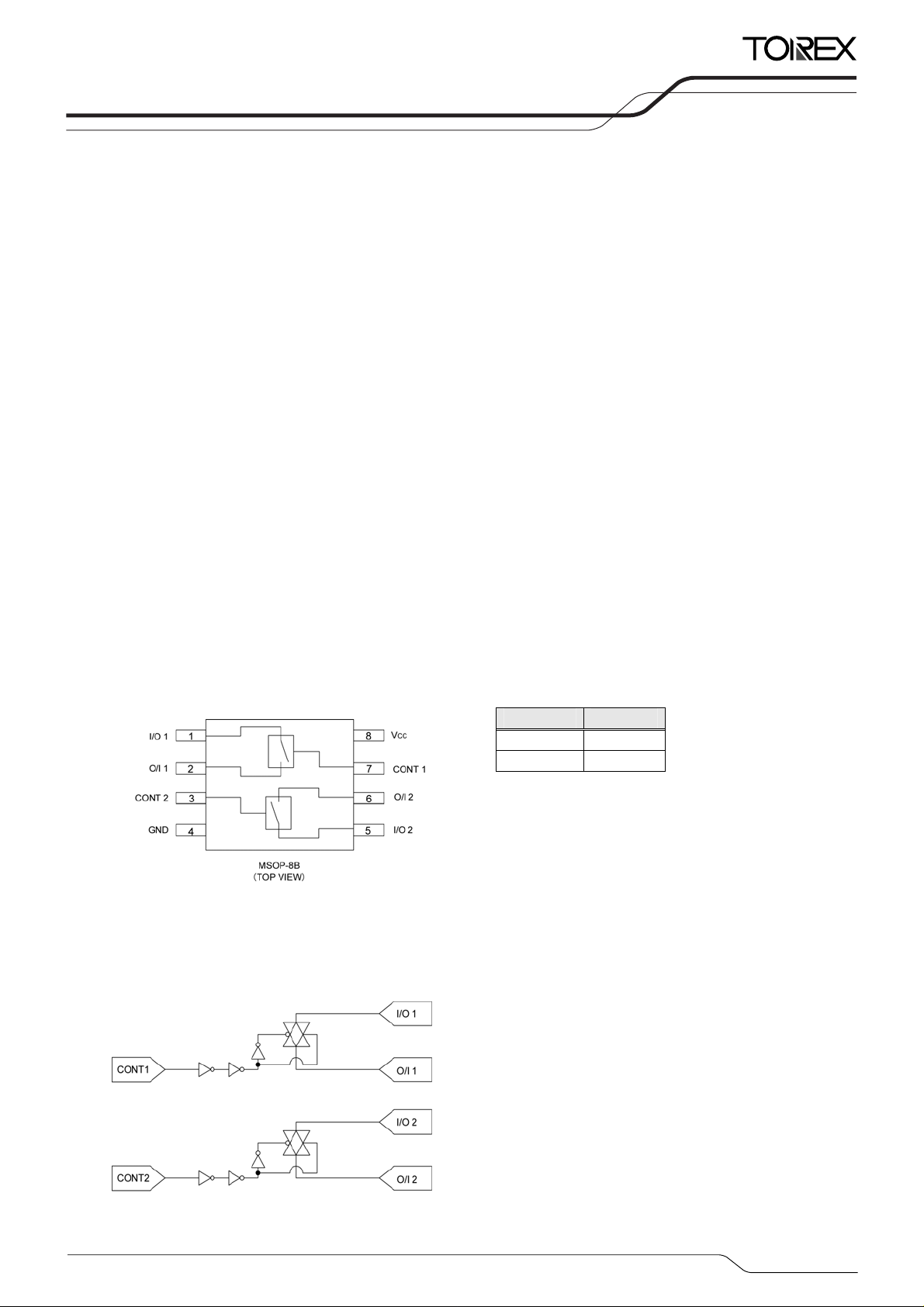
PIN CONFIGURATION
LOGIC DIAGRAM
FEATURES
High Speed Operations : tpd = 1.5ns (TYP.) (VCC=5V)
Operating Voltage Range : 2V ~ 5.5V
Low Power Consumption : 2μA (MAX.)@Ta=25℃
Low ON Resistance
CMOS Logic Dual Analog Switch
Small Package : MSOP-8B
:12Ω(TYP.)
■FUNCTIONS
CONTROL ST ATE
L OFF
H ON
H=High level
L=Low level
1/11

■
■
XC74WL4066SR
■ABSOLUTE MAXIMUM RATINGS
PARAMETER SYMBOL RATINGS UNITS
Supply Voltage VCC -0.5~+6.0 V
Input Voltage VCONT -0.5~+6.0 V
Output Voltage Vi/o -0.5~VCC+0.5 V
Input Diode Current IIK -20 mA
Output Diode Current IOK ±20 mA
Switch Output Current Ii/O ±25 mA
VCC,GND Current ICC,IGND ±50 mA
Power Dissipation (Ta = 25℃) Pd 300 mW
Storage Temperature Range Tstg -65~+150 ℃
Note : Voltage is all ground standardized.
RECOMMENDED OPERATING CONDITIONS
PARAMETER SYMBOL CONDITIONS UNITS
Supply Voltage VCC 2~5.5 V
Input Voltage VCONT 0~5.5 V
Output Voltage Vi/o 0~VCC V
Operating Temperature Range Topr -40~+85
Input Rise and Fall Time tr,tf
DC ELECTRICAL CHARACTERISTICS
0~200(VCC=3.3V)
0~100(VCC=5V)
Ta=-40℃~85℃
℃
ns
PARAMETER SYMBOL
High Level
Control Input Voltage
Low Level
Control Input Voltage
Peak ON Resistance RONmax
ON Resistance RON(1)
Switch ON Resistance
Differential
Power Off Leak Current IS(OFF) 5.5 VCONT=VIL, VIN=VCC, VOUT=GND
Power On Leak Current IS(ON) 5.5 VCONT=VIH, VIN=VCC, OR GND
Control Input Current ICONT 0~5.5 VIN=VCC or GND
Static Supply Current ICC 5.5 VIN=VCC or GND
V
V
△R
IH
IL
ON
VCC(V)
2.0 1.50
3.0 2.10
5.5
2.0
3.0
5.5
2.0 VCONT=VIH
3.0
V
IN/OUT=1mA
4.5 I
2.0 VCONT=VIH
3.0 VIN=GND or VCC
IN/OUT=1mA
4.5 I
2.0 VCONT=VIH
3.0 VIN=0~VCC
IN/OUT=1mA
4.5 I
CONDITIONS
IN=0~VCC
Ta=25℃ Ta=-40℃~85℃
MIN. TYP. MAX. MIN. MAX.
0.50
0.90
1.65
2.0
1.50
2.10
3.85
−
−
−
−
−
−
−
−
−
−
−
−
−
− −
− −
3.85
− −
− −
− −
− −
130 350
−
22 50
−
12 25
−
23 50
−
14 30
−
10 20
−
13 35
−
−
−
− − ±0.1 − ±1.0 μA
− − ±0.1 − ±1.0 μA
− − ±0.1 − ±1.0 μA
− −
3 6
2 4
UNITS
−
−
−
0.50
0.90
1.65
550
65
35
65
40
25
55
8
6
20.0
V
V
Ω
Ω
Ω
μA
2/11
■
SWITCHING ELECTRICAL CHARACTERISTICS
PARAMETER
SYMBOL
CL VCC(V)
CONDITIONS
2.0
Delay Time
15pF
PLH
t
t
PHL
50pF
3.3
5.0
2.0
3.3
5.0
2.0
Output Enable Time
15pF
t
ZL
t
ZH
50pF
3.3
5.0
2.0
3.3
R
L=1kΩ
R
L=1kΩ
5.0
2.0
Output Disable Time
15pF
t
LZ
t
HZ
50pF
3.3
5.0
2.0
3.3
R
L=1kΩ
R
L=1kΩ
5.0
XC74WL4066SR
Ta=25℃ Ta=-40℃~85℃
MIN. TYP. MAX. MIN. MAX.
−
−
−
−
−
−
−
−
−
−
−
−
−
−
−
−
−
−
2.5 12.0
2.0 4.0
1.5 3.0
4.0 20.0
3.0 6.0
2.0 5.0
8.5 45.0
4.5 9.0
3.5 7.5
9.0 50.0
5.0 10.0
4.0 8.5
9.0 45.0
7.0 17.0
6.0 14.0
12.0 60.0
10.0 23.0
8.0 20.0
−
−
−
−
−
−
−
−
−
−
−
−
−
−
−
−
−
−
15.0
5.5
4.0
23.0
8.0
6.0
60.0
11.0
9.0
65.0
12.0
10.0
55.0
20.0
18.0
75.0
27.0
25.0
(tr=tf=3ns)
UNITS
ns
ns
ns
ns
ns
ns
Sine Wave Distortion Rate 50pF 3.0
-3dB Band Width 50pF 3.0
Feed Through
(Switch off)
Cross Talk
(Control Switches)
Cross Talk
(Between Switches)
50pF 3.0
50pF
50pF
Control Input Capacitance CCONT
Switch Input/Output Capacitance CIN/OUT
Feed Through Capacitance CIN-OUT
Power Dissipation Capacitance Cpd
2.0
3.0
4.5
2.0
3.0
4.5
− −
− −
− −
− −
R
L=10kΩ
f
IN=1kHz
RL=600Ω
20log10
VOUT
=-3dB
IN
V
R
L=600Ω −
R
L=600Ω
f
CONT=1MHz
R
L=600Ω
f
IN=1MHz
−
−
−
−
−
−
−
−
−
−
−
−
0.05
200
-60
60
100
150
-60
-60
-60
− − −
− − −
− − −
− − −
− − −
− − −
− − −
− − −
− − −
5 10
6
− − −
0.5
13
− − −
− − −
−
%
MHz
dB
mV
dB
10 pF
pF
pF
pF
3/11
■
XC74WL4066SR
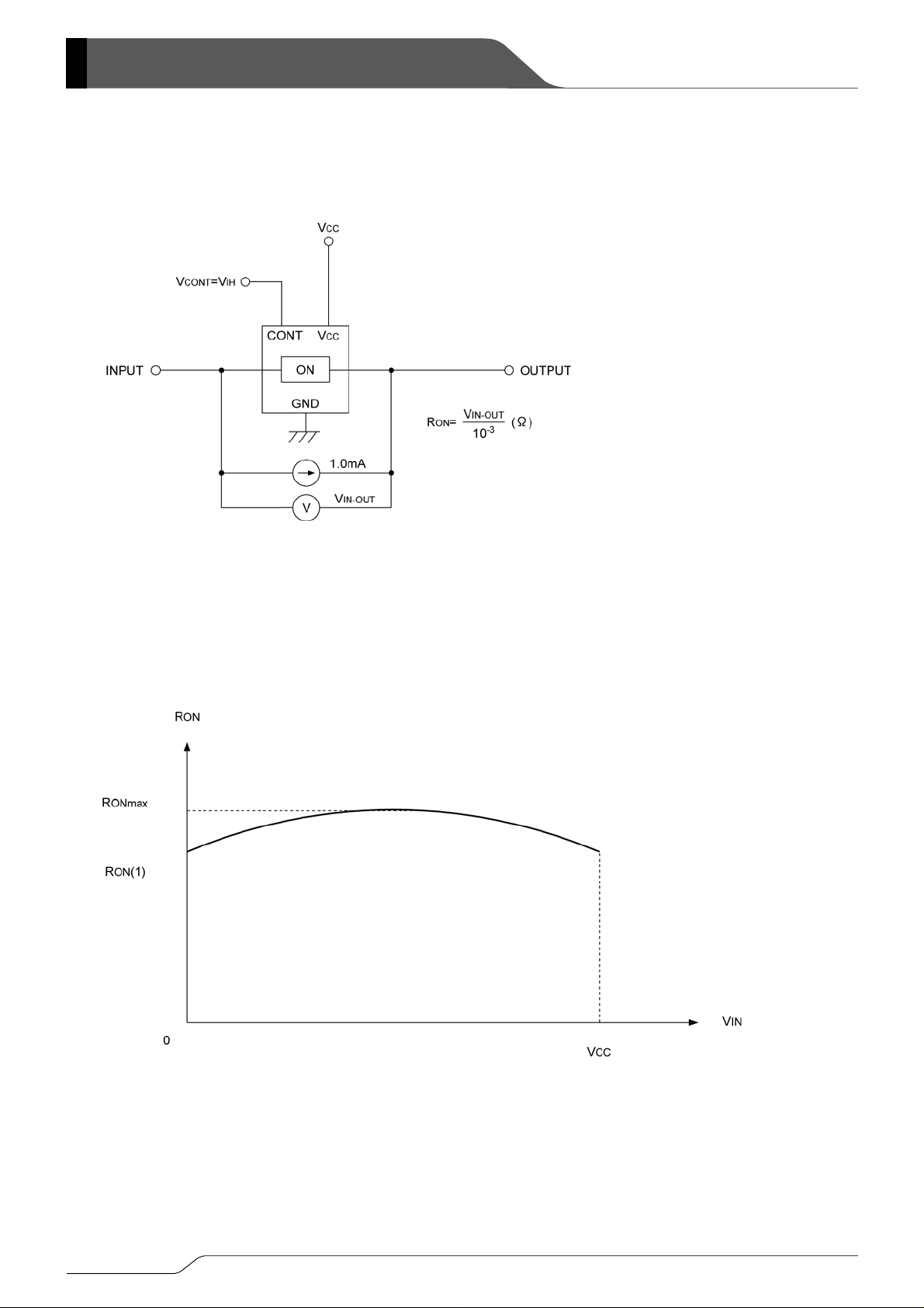
ON RESISTANCE
●Test Circuit
●Input Voltage Dependancies of ON Resistance
4/11

■
■
POWER OFF LEAK CURRENT
POWER ON LEAK CURRENT
XC74WL4066SR
5/11

■
XC74WL4066SR
DELAY TIME
●Test Circuit
●Waveform
6/11

■
OUTPUT ENABLE TIME, OUTPUT DISABLE TIME
●Test Circuit
●Waveform
XC74WL4066SR
7/11

■
■
XC74WL4066SR
SINE WAVE DISTORTION RATE
-3dB BAND WIDTH
8/11

■
■
→
FEED THROUGH TEST CIRCUIT
CROSS TALK (CONTROL INPUT
●Test Circuit
●Waveform
XC74WL4066SR
SWITCH OUTPUT)
9/11

■
XC74WL4066SR
CROSS TALK (BETWEEN SWITCHES)
●Test Circuit
●Waveform
10/11

XC74WL4066SR
1. The products and product specifications contained herein are subject to change without
notice to improve performance characteristics. Consult us, or our representatives
before use, to confirm that the information in this datasheet is up to date.
2. We assume no responsibility for any infringement of patents, patent rights, or other
rights arising from the use of any information and circuitry in this datasheet.
3. Please ensure suitable shipping controls (including fail-safe designs and aging
protection) are in force for equipment employing products listed in this datasheet.
4. The products in this datasheet are not developed, designed, or approved for use with
such equipment whose failure of malfunction can be reasonably expected to directly
endanger the life of, or cause significant injury to, the user.
(e.g. Atomic energy; aerospace; transport; combustion and associated safety
equipment thereof.)
5. Please use the products listed in this datasheet within the specified ranges.
Should you wish to use the products under conditions exceeding the specifications,
please consult us or our representatives.
6. We assume no responsibility for damage or loss due to abnormal use.
7. All rights reserved. No part of this datasheet may be copied or reproduced without the
prior permission of TOREX SEMICONDUCTOR LTD.
11/11
 Loading...