

Torex XC74WL02AASR User Manual
XC74WL02AASR
ETR1312_001
CMOS Logic
■GENERAL DESCRIPTION
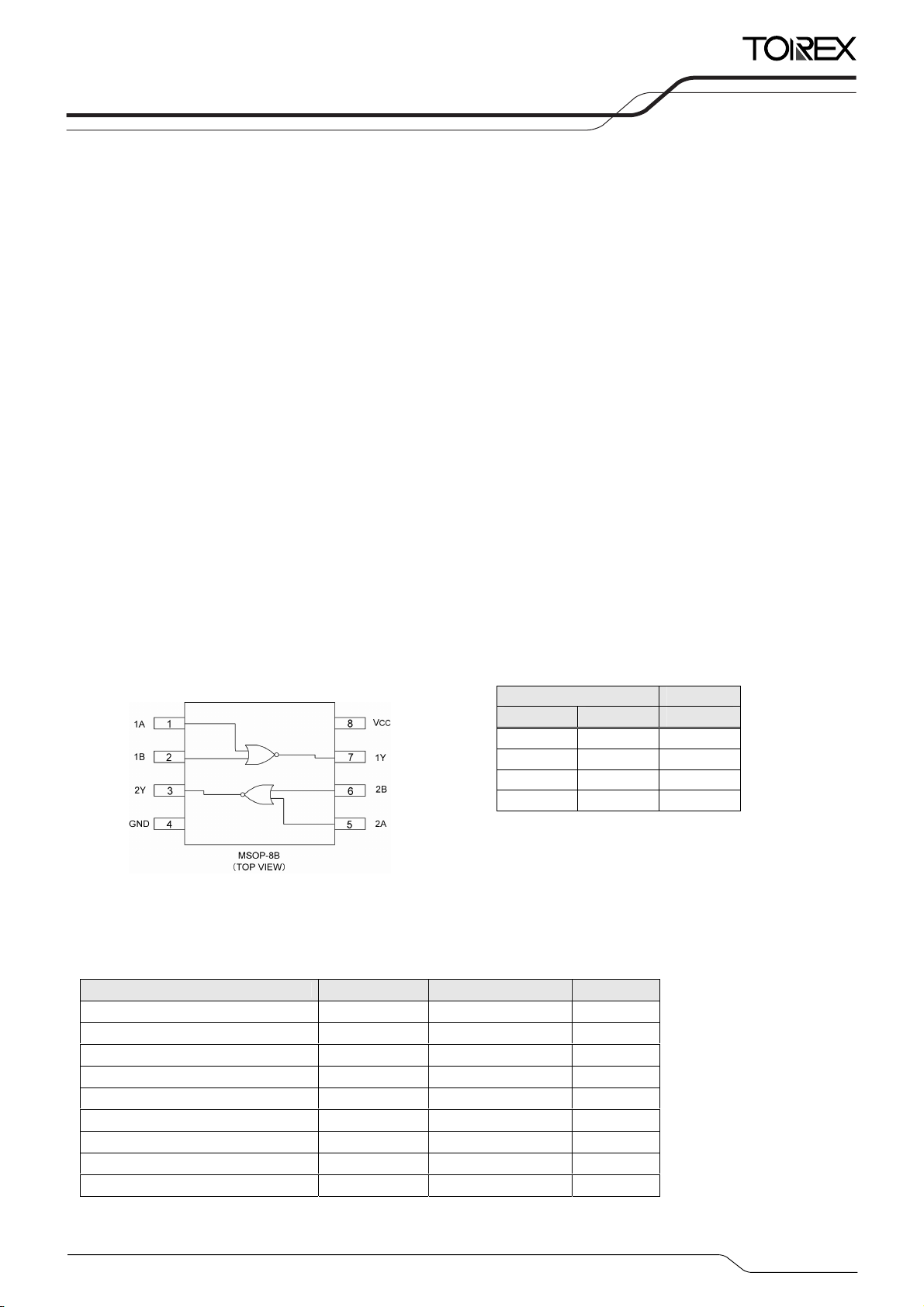
XC74WL02AASR is dual 2-input NOR Gate manufactured using silicon gate CMOS processes. The small supply current,
which is one of the features of the CMOS logic, gives way to high speed operations which enables LS-TTL.
With wave forming buffers connected internally, stabilized output can be achieved as the series offers high noise immunity.
As the series is integrated into a mini molded, MSOP-8B package, high density mounting is possible.
■APPLICATIONS
●Palmtops
●Digital equipment
■PIN CONFIGURATION
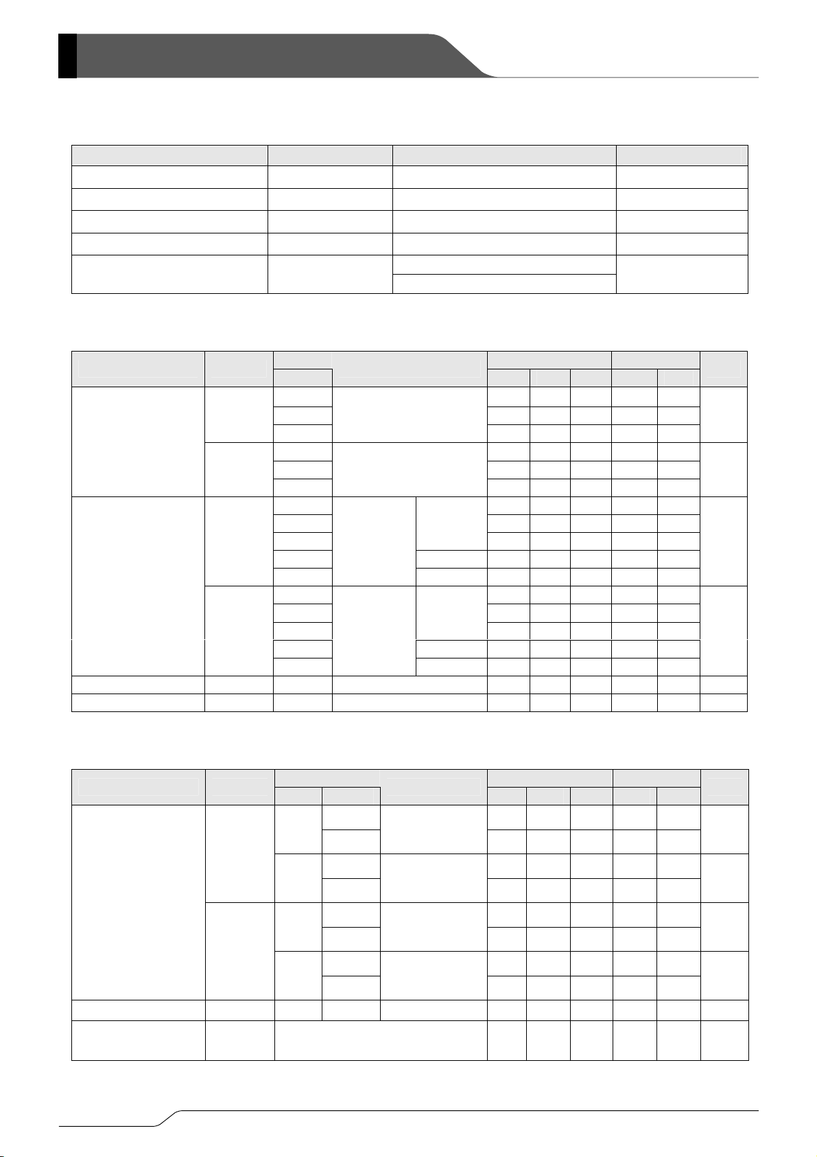
■ABSOLUTE MAXIMUM RATINGS
PARAME T E R SYMBOL RATINGS UNITS
Power Supply Voltage VCC -0.5~+6.0 V
Input Voltage VIN -0.5~+6.0 V
Output Voltage VOUT -0.5~VCC+0.5 V
Input Diode Current IIK -20 mA
Output Diode Current IOK ±20 mA
Switch Output Current IOUT ±25 mA
VCC,GND Current ICC,IGND ±50 mA
Power Dissipation (Ta = 25℃) Pd 300 mW
Storage Temperature Range Tstg -65~+150 ℃
Note : Voltage is all ground standardized.
■FEATURES
High Speed Operations : tpd = 2.65ns (TYP.) (VCC=5V)
Operating Voltage Range : 2V ~ 5.5V
Low Power Consumption : 1μA (MAX.)@Ta=25℃
CMOS Logic Dual 2-Input NOR Gate
Small Package : MSOP-8B
■FUNCTIONS
INPUT OUTPUT
A B Y
H H L
H L L
L H L
L L H
H=High level
L=Low level
Ta =- 40 ℃~85℃
1/4
XC74WL02AASR
■RECOMMENDED OPERATING CONDITIONS
PARAMETER SYMBOL CONDITIONS UNITS
Supply Voltage VCC 2~5.5 V
Input Voltage VIN 0~5.5 V
Output Voltage VOUT 0~ VCC V
Operating Temperature Range Topr -40~+85
Input Rise and Fall Time tr,tf
■DC ELECTRICAL CHARACTERISTICS
PARAMETER SYMBOL
VIH
Input Voltage
IL
V
VOH
Output Voltage
OL
V
Input Current IIN
Static Supply Current ICC 5.5
■SWITCHING ELECTRICAL CHARACTERISTICS
PARAMETER SYMBOL
tPLH
Delay Time
tPHL
Input Capacitance CIN
Power Dissipation
Capacitance
Cpd No Load, f=1MHz
VCC(V)
2.0 1.5
3.0 2.1
5.5
2.0
3.0
5.5
2.0 1.9 2.0
3.0 2.9 3.0
4.5
3.0 IOH=-4mA 2.58
4.5
2.0
3.0
4.5
3.0 IOL=4mA
4.5
0~5.5
CL VCC(V)
15pF
50pF
15pF
50pF
-
CONDITIONS
VIN=VIL
VIN=VIL or VIH
VIN=VCC or GND -0.1
V
IN=VCC or GND,IOUT=0μA - -
CONDITIONS
3.3
5.0
3.3
5.0
3.3
5.0
3.3
5.0
5.0 VIN=VCC or GND
0~200(VCC=3.3V)
0~100(VCC=5V)
I
OH=-50μA
OH=-8mA 3.94
I
OL=50μA
I
IOL=8mA
MIN. TYP. MAX. MIN. MAX.
3.85
- -
- -
- -
4.4 4.5
- -
- -
- -
- -
- -
MIN. TYP. MAX. MIN. MAX.
-
-
-
-
-
-
-
-
-
-
℃
ns
Ta =2 5℃ Ta =- 40 ℃~85℃
- -
- -
- -
0.5
0.9
1.65
-
-
-
- -
- -
0.1
0.1
0.1
0.36
0.36
0.1 -1.0 1.0
-
1.0
Ta =2 5℃ Ta =- 40 ℃~85℃
3.9 7.9 1.0 9.5
2.7 5.5 1.0 6.5
5.5 11.4 1.0 13
3.9 7.5 1.0 8.5
3.5 7.9 1.0 9.5
2.6 5.5 1.0 6.5
4.9 11.4 1.0 13
3.6 7.5 1.0 8.5
4 10
9.7
- - -
1.5
2.1
3.85
-
-
-
1.9
2.9
4.4
2.48
3.80
-
-
-
-
-
-
-
-
-
-
0.5
0.9
1.65
-
-
-
-
-
0.1
0.1
0.1
0.44
0.44
10.0
10 pF
UNITS
V
V
V
V
μA
μA
(tr=tf=3ns)
UNITS
ns
ns
ns
ns
pF
2/4
 Loading...