

XC6701 Series
ETR0334-008a
28V Operation High Speed Voltage Regulators with Stand-by Function
■GENERAL DESCRIPTION
The XC6701 series are positive voltage regulator ICs manufactured using CMOS process with 28V of operation voltage.
The series consists of a voltage reference, an error amplifier, a current limiter, a thermal protection circuit and a phase
compensation circuit plus a driver transistor.
The output voltage is selectable in 0.1V increments within the range of 1.8V to 18V which fixed by laser trimming
technologies. The output stabilization capacitor (C
The over current protection circuit and the thermal shutdown circuit are built-in. These two protection circuits will operate
when the output current reaches current limit level or the junction temperature reaches temperature limit level.
The CE function enables the output to be turned off and the IC becomes a stand-by mode resulting in greatly reduced power
consumption. Packages are selectable depending on the applications from SOT-25, SOT-89, SOT-89-5, USP-6C, SOT-223,
and TO-252.
■APPLICATIONS
●Car audio, Car navigation systems
●Note book computers, PDAs
●Home appliances
●Audio visuals, Digital cameras, Video cameras
●Cordless phones, Wireless communication
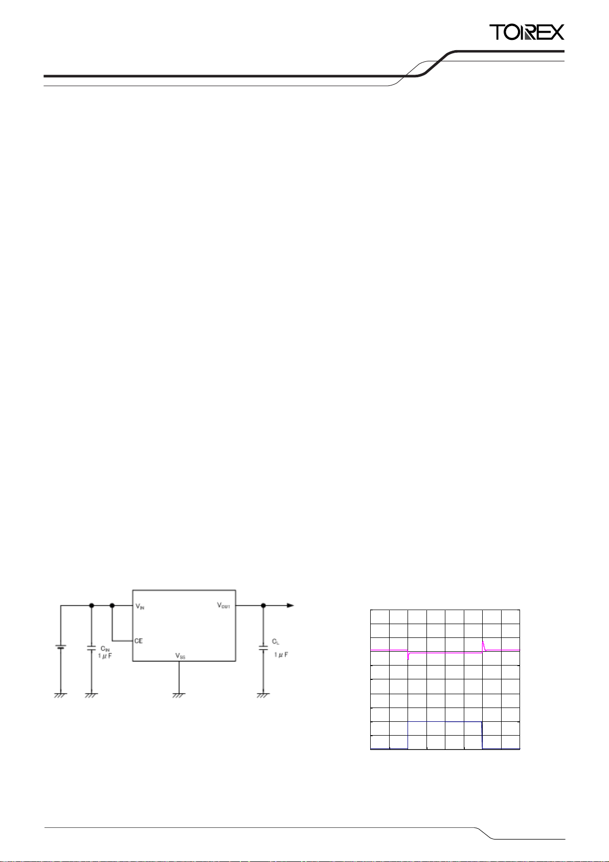
■ TYPICAL APPLICATION CIRCUITS
XC6701B Series
With CE function
) is also compatible with low ESR ceramic capacitors.
L
■FEATURES
Max Output Current : More than 150mA (200mA limit)
(V
Dropout Voltage : 300mV@I
Input Voltage Range : 2.0V~28.0V
Output Voltage Range : 1.8V~18.0V (0.1V increments)
High Accuracy :±2%
Low Power Consumption : 50μA (V
Stand-by Current : Less than 0.1μA
High Ripple Rejection : 50dB@1kHz
Operating Temperature : -40℃~+85℃
Low ESR Capacitor : Ceramic Capacitor Compatible
(Internal Phase Compensation)
Packages : SOT-25, SOT-89, SOT-89-5,
Environmentally Friendly
USP-6C, SOT-223, TO-252
: EU RoHS Compliant, Pb Free
IN=VOUT
+3.0V)
OUT
OUT
■ TYPICAL PERFORMANCE
CHARACTERISTICS
XC6701B/D 502
VIN=7.0V, tr =tf=5μs
C
=1. 0μF (ce ram ic), Ta =25℃
5.6
5.4
5.2
(V)
5.0
OUT
4.8
4.6
4.4
4.2
Output Voltage: V
4.0
3.8
3.6
IN=CL
Output Voltage
Output Current
Time (1ms/div)
=20mA
=5.0V)
150
120
90
60
30
0
(mA)
OUT
Output Current: I
1/35
XC6701 Series
■PIN CONFIGURATION
■PIN ASSIGNMENT
●XC6701B Series
SOT-25 SOT-89-5 USP-6C
●XC6701D Series
SOT-89 SOT-223 TO-252
■PIN FUNCTION ASSIGNMENT
●XC6701B Series
SOT-25
(TOP VIEW)
SOT-223
(TOP VIEW)
PIN NUMBER
1 5 6 VIN Power Input
2 2 5 VSS Ground
3 4 2, 4 NC No connection
4 3 3 CE ON/OFF Control
5 1 1 V
PIN NUMBER
3 3 1 VIN Power Input
2 2 2 VSS Ground
1 1 3 V
CE(Chip Enable) IC Operation State ON/OFF
CE"H" Level Operation ON
CE"L" Level Operation OFF
CE"OPEN" Operation Undefined
SOT-89
(TOP VIEW)
TO-252
(TOP VIEW)
PIN NAME FUNCTIONS
Output
OUT
PIN NAME FUNCTIONS
Output
OUT
SOT-89-5
(TOP VIEW)
USP-6C
(BOTTOM VIEW)
* The dissipation pad for the USP-6C
package should be solder-plated in
reference mount pattern and metal
masking so as to enhance mounting
strength and heat release. If the
pad needs to be connected to other
pins, it should be connected to the
V
(No. 5) pin.
SS
2/35
■ PRODUCT CLASSIFICATION
●Ordering Information
XC6701B①②③④⑤-⑥
DESIGNATOR ITEM SYMBOL DESCRIPTION
①②
③
④⑤-⑥
(*1)
The “-G” suffix indicates that the products are Halogen and Antimony free as well as being fully RoHS compliant.
XC6701D①②③④⑤-⑥
DESIGNATOR ITEM SYMBOL DESCRIPTION
①②
③
④⑤-⑥
(*1)
The “-G” suffix indicates that the products are Halogen and Antimony free as well as being fully RoHS compliant.
(*1)
:CE function (Active High)
Output Voltage 18~J0
Output Voltage
Accuracy
2
MR SOT-25 (3,000/Reel)
MR-G SOT-25 (3,000/Reel)
Packages
(Order Unit)
PR SOT-89-5 (1,000/Reel)
PR-G SOT-89-5 (1,000/Reel)
ER USP-6C (3,000/Reel)
ER-G USP-6C (3,000/Reel)
(*1)
: No CE function (3 pin regulator)
Output Voltage 18~J0
Output Voltage
Accuracy
2
PR SOT-89 (1,000/Reel)
PR-G SOT-89 (1,000/Reel)
Packages
(Order Unit)
FR SOT-223 (1,000/Reel)
FR-G SOT-223 (1,000/Reel)
JR TO-252 (2,500/Reel)
JR-G TO-252 (2,500/Reel)
For the voltage within 1.8V ~9.9V;
e.g. 2.5V ⇒ 25
5.0V ⇒ 50
For the voltage above 10.0V;
e.g. 11.6V ⇒ B6
15.2V ⇒ F2
18.0V ⇒ J0
±2% accuracy
For the voltage within 1.8V ~9.9V;
e.g. 2.5V ⇒ 25
5.0V ⇒ 50
For the voltage above 10.0V;
e.g. 11.6V ⇒ B6
15.2V ⇒ F2
18.0V ⇒ J0
±2% accuracy
XC6701
Series
3/35
XC6701 Series
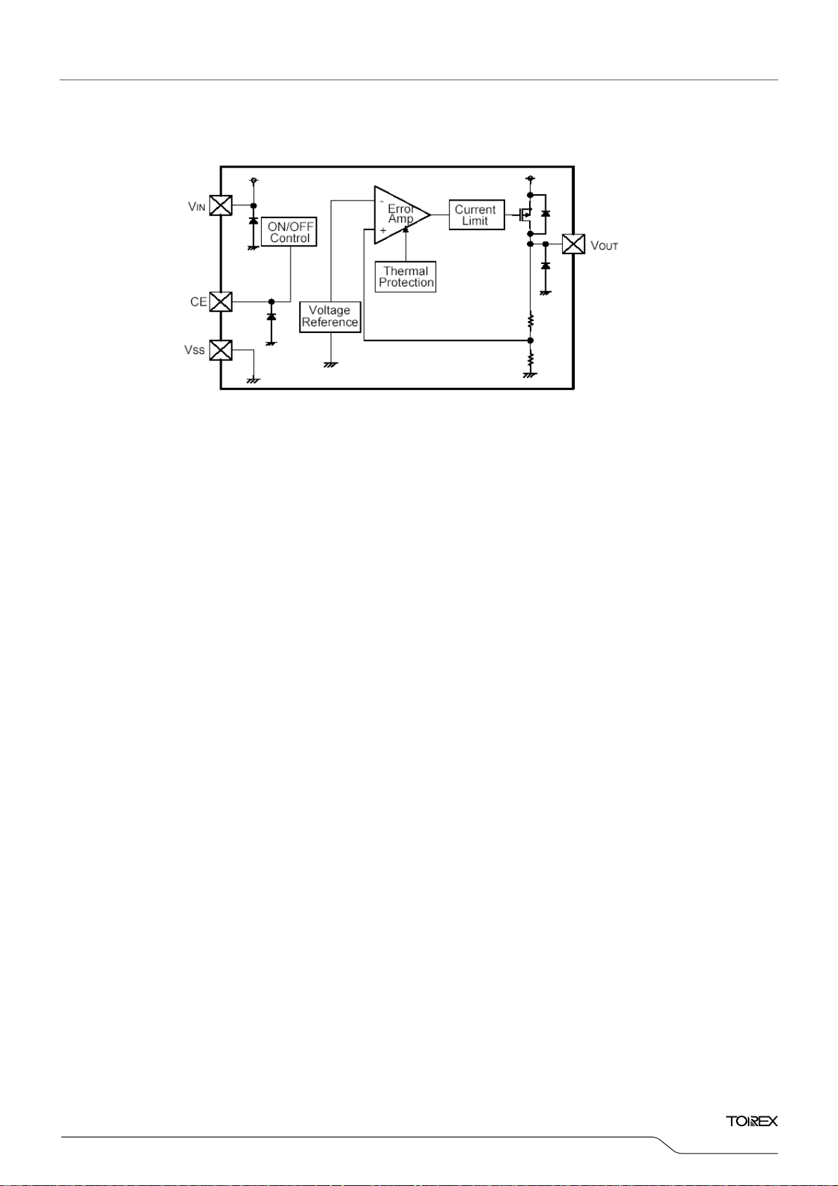
■ BLOCK DIAGRAMS
●XC6701B Series
(SOT-25, SOT-89-5, USP-6C)
■ABSOLUTE MAXIMUM RATINGS
●XC6701B Series
PAR AMETER SYMBOL RATINGS UNIT
Input Voltage VIN V
Output Current I
Output Voltage V
300
OUT
V
OUT
CE Input Voltage VCE V
SOT-25
Power Dissipation
SOT-89-5
Pd
USP-6C
Operating Temperature Range Topr -40~+85
Storage Temperature Range Tstg -55~+125
*1: I
≦Pd / (VIN-V
OUT
*2: The power dissipation figure shown is PCB mounted. Please refer to page 27 for details.
●XC6701D Series
OUT
)
PAR AMETER SYMBOL RATINGS UNIT
Input Voltage VIN V
Output Current I
Output Voltage V
300
OUT
V
OUT
SOT-89
Power Dissipation
SOT-223
Pd
TO-252
Operating Temperature Range Topr -40~+85
Storage Temperature Range Tstg -55~+125
*1: I
≦Pd / (VIN-V
OUT
*2: The power dissipation figure shown is PCB mounted. Please refer to page 27 for details.
OUT
)
●XC6701D Series
(SOT-89, SOT-223, TO-252)
-0.3~30 V
SS
(*1)
mA
-0.3~VIN+0.3 V
SS
-0.3~30 V
SS
250
600 (PCB mounted)
500
1300 (PCB mounted)
120
1000 (PCB mounted)
-0.3~30 V
SS
(*1)
mA
-0.3~VIN+0.3 V
SS
500
1000 (PCB mounted)
300
1500 (PCB mounted)
500
1800 (PCB mounted)
(*2)
(*2)
(*2)
(*2)
(*2)
(*2)
mW
(Ta=25℃)
℃
℃
mW
(Ta=25℃)
℃
℃
4/35
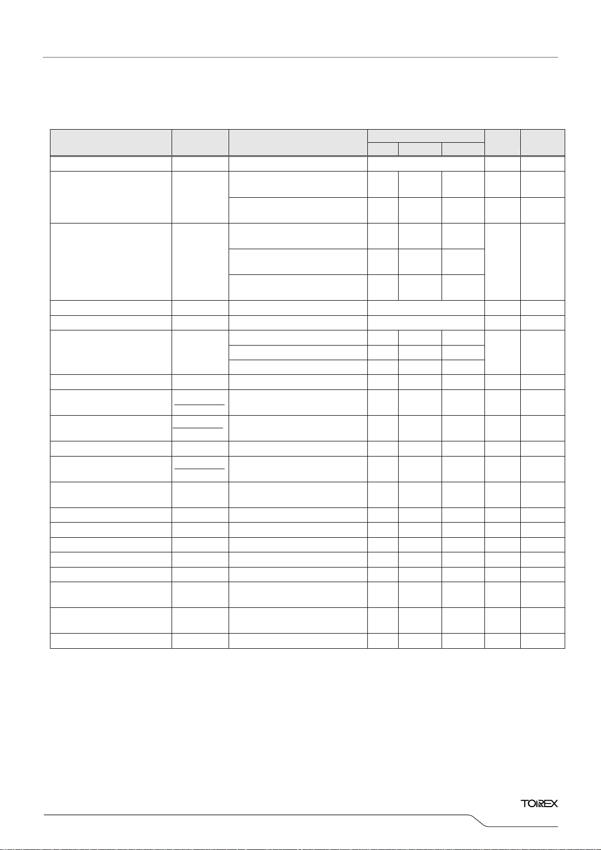
■ELECTRICAL CHARACTERISTICS
●XC6701B Series
PAR AMETER SYMBOL CONDITIONS
Output Voltage V
Maximum Output Current I
I
OUT(E)
VIN= V
OUTMAX
1mA≦I
=10mA, VCE=VIN E-0 V
OUT
OUT(T)
(V
OUT(T)
V
IN=VOUT(T)
(V
OUT(T)
≦50mA , VCE=VIN
OUT
1.8V≦V
Load Regulation
△V
OUT
1mA≦I
1mA≦I
≦50mA , VCE=VIN
OUT
5.1V≦V
OUT(T)
≦50mA , VCE=VIN
OUT
12.1V≦V
Dropout Voltage 1 Vdif1 I
Dropout Voltage 2 Vdif2 I
=20mA, VCE=VIN
OUT
=100mA ,VCE=VIN
OUT
1.8V≦V
Supply Current ISS
5.1V≦V
OUT(T)
12.1V≦V
Stand-by Current I
Line Regulation 1
Line Regulation 2
△VIN・V
△V
V
STB
△V
OUT
OUT(T)
△V
OUT
IN・VOUT(T)
V
OUT(T)
V
OUT(T)
I
CE=VSS
+2.0V≦VIN≦28.0V
I
=5mA , VCE=VIN
OUT
+2.0V≦VIN≦28.0V
=13mA , VCE=VIN
OUT
Input Voltage VIN
Output Voltage
Temperature Characteristics
△Ta ・V
Ripple Rejection Rate PSRR
Short Current I
CE ”H” Level Voltage V
CE ”L” Level Voltage V
CE ”H” Level Current I
CE ”L” Level Current I
Thermal Shutdown
Detect Temperature
Thermal Shutdown Release
Temperature
Hysteresis Width T
NOTE:
*1: V
*2: V
(i.e. the output voltage when “V
*3: Vdif={V
*4: V
: In case of V
*5: V
*6: Unless otherwise stated, V
: Nominal output voltage
OUT(T)
: Effective output voltage
OUT(E)
{Note 5}
IN1
: In case of V
OUT1
: The input voltage when V
IN1
- V
OUT1
{Note 4}
< 3.0V, the V
OUT(T)
OUT(T)
}
≧3.0V, the V
OUT1
IN=VOUT(T)
△V
OUT
OUT(T)
V
SHORT
V
CEH
V
CEL
V
CEH
V
CEL
T
Junction Temperature - 150 -
TSD
T
Junction Temperature - 125 -
TSR
TSD-TTSR
appears as input voltage is gradually decreased.
Junction Temperature - 25 -
+2.0V” is provided at the VIN pin while maintaining a certain I
OUT(T)
is equal to 98% of the V
OUT1
is equal to 98% of the V
OUT1
+2.0V.
I
=20mA, VCE=VIN
OUT
VIN=[V
-40℃≦Ta ≦85℃
+2.0V]VDC+0.5V
OUT(T)
I
=20mA , f=1kHz , VCE=VIN
OUT
IN=VOUT(T)
+2.0V , VCE=VIN
IN
IN
IN=VCE
=28.0V, VCE=VSS
IN
Ta =2 5℃
MIN. TYP. MAX.
+3.0V , VCE=VIN
≧3.0V)
+3.0V, VCE=VIN
<3.0V)
≦5.0V
OUT(T)
≦12.0V
≦18.0V
OUT(T)
150 - -
100 - -
- 50 90
- 110 175
- 180 275
E-2
E-3
OUT(T)
OUT(T)
≦5.0V
≦12.0V
≦18.0V
11 50 105
11 60 115
11 65 125
- 0.01 0.10
- 0.05 0.10
- 0.15 0.30
2.0 - 28.0
- ±100 -
P-PAC
- 50 -
- 40 -
=28.0V
=28.0V
=28.0V
1.1 - 28.0
0 - 0.35
-0.1 - 0.1
-0.1 - 0.1
when a stabilized input voltage is applied in V
OUT(T)
when a stabilized input voltage is applied in V
OUT(T)
OUT
value.)
XC6701
Series
UNIT CIRCUIT
mA
mA
mV
mV
mV
μA ②
μA ②
%/V ①
%/V ①
V -
ppm/℃ ①
dB
mA
V
V
μA ①
μA ①
℃ ①
℃ ①
℃
+3.0V.
OUT(T)
+2.0V.
OUT(T)
①
①
①
①
①
①
③
①
①
①
-
5/35
XC6701 Series
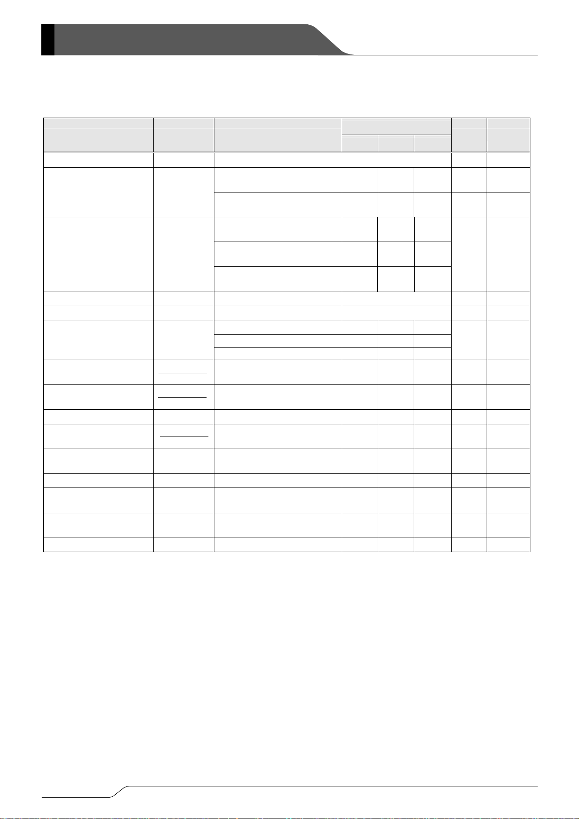
■ELECTRICAL CHARACTERISTICS (Continued)
●XC6701D Series
PAR AMETER SYMBOL CONDITIONS
Output Voltage V
Maximum Output Current I
Load Regulation
I
OUT(E)
OUTMAX
△V
OUT
Dropout Voltage1 Vdif1 I
Dropout Voltage2 Vdif2 I
Supply Current ISS
△V
Line Regulation1
Line Regulation2
△V
IN・VOUT(T)
△V
△VIN・V
OUT
OUT
OUT(T)
Input Voltage VIN
Output Voltage
Temperature Characteristics
△V
△Ta ・V
OUT
OUT(T)
Ripple Rejection Rate PSRR
Short Current I
Thermal Shutdown Detect
Temperature
Thermal Shutdown Release
Temperature
Hysteresis Width T
NOTE:
*1: V
*2: V
(i.e. the output voltage when “V
*3: Vdif={V
*4: V
: In case of V
*5: V
*6: Unless otherwise stated, V
: Nominal output voltage
OUT(T)
: Effective output voltage
OUT(E)
{Note 5}
IN1
: In case of V
OUT1
: The input voltage when V
IN1
- V
OUT1
{Note 4}
< 3.0V, the V
OUT(T)
OUT(T)
}
≧3.0V, the V
IN=VOUT(T)
V
SHORT
Junction Temperature - 150 -
T
TSD
T
Junction Temperature - 125 -
TSR
TSD-TTSR
OUT1
Junction Temperature - 25 -
OUT(T)
is equal to 98% of the V
OUT1
is equal to 98% of the V
OUT1
appears as input voltage is gradually decreased.
+2.0V.
Ta =2 5℃
MIN. TYP. MAX.
=10mA E-0 V
OUT
VIN= V
(V
OUT(T)
V
IN=VOUT(T)
(V
OUT(T)
1mA≦I
1.8V≦V
1mA≦I
5.1V≦V
1mA≦I
12.1V≦V
OUT
OUT
1.8V≦V
5.1V≦V
12.1V≦V
+2.0V≦VIN≦28.0V
V
OUT(T)
I
V
+2.0V≦VIN≦28.0V
OUT(T)
I
OUT
OUT(T)
≧3.0V)
<3.0V )
OUT
OUT(T)
OUT
OUT(T)
OUT
OUT(T)
=20mA
=100mA
OUT(T)
OUT(T)
OUT(T)
=5mA
OUT
=13mA
+3.0V
+3.0V
≦50mA
≦5.0V
≦50mA
≦12.0V
≦50mA
≦18.0V
≦5.0V
≦12.0V
≦18.0V
150 - -
100 - -
- 50 90
- 110 175
- 180 275
E-2
E-3
11 50 105
11 60 115
11 65 125
- 0.05 0.10
- 0.15 0.30
2.0 - 28.0
I
=20mA
OUT
-40℃≦Ta ≦85℃
VIN=[V
+2.0V” is provided at the VIN pin while maintaining a certain I
+2.0V]+0.5V
OUT(T)
I
=20mA , f=1kHz
OUT
IN=VOUT(T)
P-PAC
+2.0V
when a stabilized input voltage is applied in V
OUT(T)
when a stabilized input voltage is applied in V
OUT(T)
- ±100 -
- 50 -
- 40 -
value.)
OUT
UNIT CIRCUIT
①
mA
mA
mV
mV
mV
①
①
①
①
①
μA ②
%/V ①
%/V ①
V -
ppm/℃ ①
dB
mA
③
①
℃ ①
℃ ①
℃
OUT(T)
OUT(T)
+3.0V.
+2.0V.
-
6/35
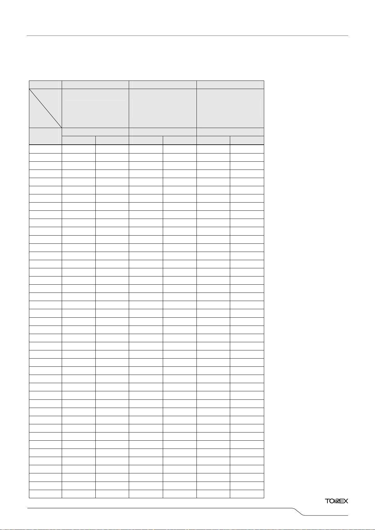
■ELECTRICAL CHARACTERISTICS (Continued)
●Voltage Chart
SYMBOL E-0 E-2 E-3
PARAMETER
NOMINAL
OUTPUT
VOLTAGE (V)
OUT(T)
(V)
1.8 1.764 1.836 550 710 2200 2700
1.9 1.862 1.938 550 710 2200 2700
2.0 1.960 2.040 450 600 1900 2600
2.1 2.058 2.142 450 600 1900 2600
2.2 2.156 2.244 390 520 1700 2200
2.3 2.254 2.346 390 520 1700 2200
2.4 2.352 2.448 390 520 1700 2200
2.5 2.450 2.550 310 450 1500 1900
2.6 2.548 2.652 310 450 1500 1900
2.7 2.646 2.754 310 450 1500 1900
2.8 2.744 2.856 310 450 1500 1900
2.9 2.842 2.958 310 450 1500 1900
3.0 2.940 3.060 260 360 1300 1700
3.1 3.038 3.162 260 360 1300 1700
3.2 3.136 3.264 260 360 1300 1700
3.3 3.234 3.366 260 360 1300 1700
3.4 3.332 3.468 260 360 1300 1700
3.5 3.430 3.570 260 360 1300 1700
3.6 3.528 3.672 260 360 1300 1700
3.7 3.626 3.774 260 360 1300 1700
3.8 3.724 3.876 260 360 1300 1700
3.9 3.822 3.978 260 360 1300 1700
4.0 3.920 4.080 220 320 1100 1500
4.1 4.018 4.182 220 320 1100 1500
4.2 4.116 4.284 220 320 1100 1500
4.3 4.214 4.386 220 320 1100 1500
4.4 4.312 4.488 220 320 1100 1500
4.5 4.410 4.590 220 320 1100 1500
4.6 4.508 4.692 220 320 1100 1500
4.7 4.606 4.794 220 320 1100 1500
4.8 4.704 4.896 220 320 1100 1500
4.9 4.802 4.998 220 320 1100 1500
5.0 4.900 5.100 190 280 1000 1300
5.1 4.998 5.202 190 280 1000 1300
5.2 5.096 5.304 190 280 1000 1300
5.3 5.194 5.406 190 280 1000 1300
5.4 5.292 5.508 190 280 1000 1300
5.5 5.390 5.610 190 280 1000 1300
5.6 5.488 5.712 190 280 1000 1300
5.7 5.586 5.814 190 280 1000 1300
5.8 5.684 5.916 190 280 1000 1300
5.9 5.782 6.018 190 280 1000 1300
6.0 5.880 6.120 190 280 1000 1300
OUTPUT VOLTAGE(V)
(2% products)
V
MIN. MAX. TYP. MAX. TYP. MAX.
OUT
Vdif1 Vdif2 V
DROPOUT VOLTAGE 1
I
OUT
(mV)
=20mA
DROPOUT VOLTAGE 2
I
OUT
(mV)
=100mA
XC6701
Series
7/35
XC6701 Series
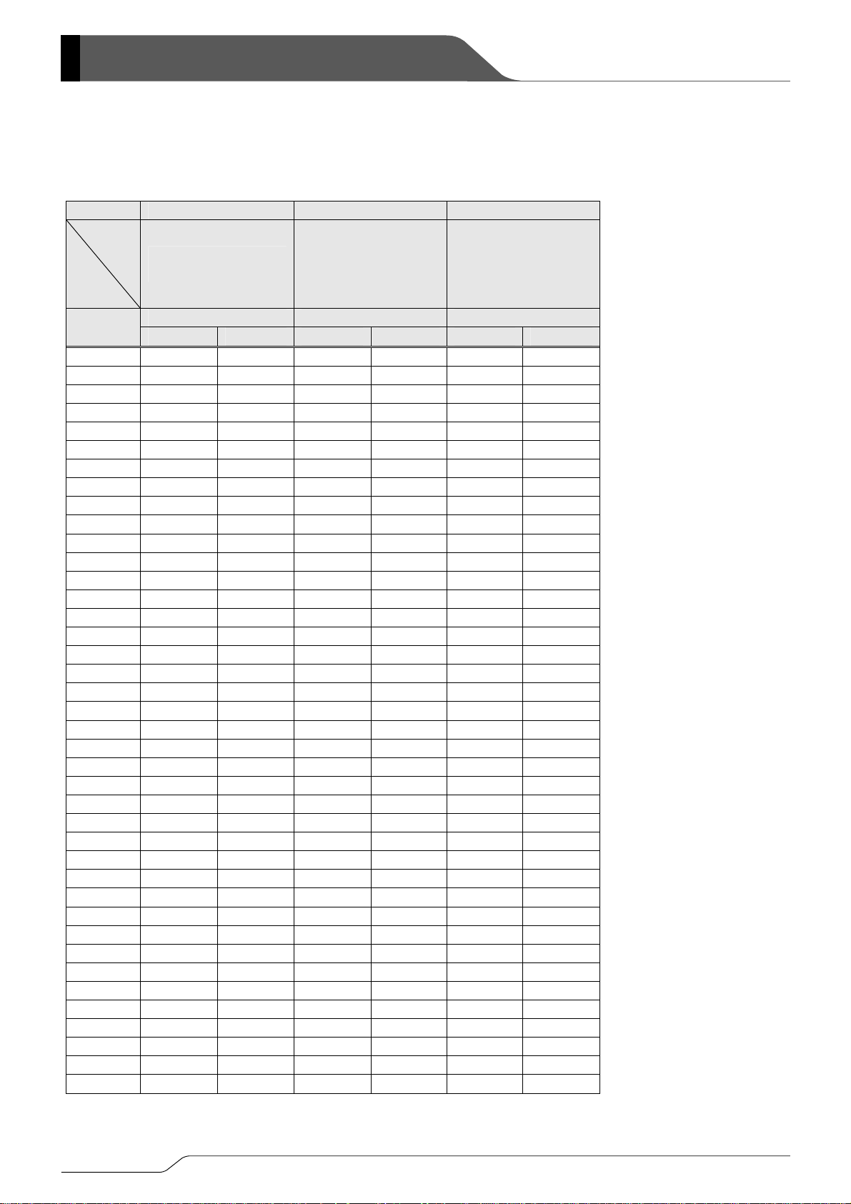
■ELECTRICAL CHARACTERISTICS (Continued)
●Voltage Chart (Continued)
SYMBOL E-0 E-2 E-3
PARAMETER
NOMINAL
OUTPUT
VOLTAGE (V)
OUT(T)
(V)
6.1 5.978 6.222 190 280 1000 1300
6.2 6.076 6.324 190 280 1000 1300
6.3 6.174 6.426 190 280 1000 1300
6.4 6.272 6.528 190 280 1000 1300
6.5 6.370 6.630 170 230 800 1150
6.6 6.468 6.732 170 230 800 1150
6.7 6.566 6.834 170 230 800 1150
6.8 6.664 6.936 170 230 800 1150
6.9 6.762 7.038 170 230 800 1150
7.0 6.860 7.140 170 230 800 1150
7.1 6.958 7.242 170 230 800 1150
7.2 7.056 7.344 170 230 800 1150
7.3 7.154 7.446 170 230 800 1150
7.4 7.252 7.548 170 230 800 1150
7.5 7.350 7.650 170 230 800 1150
7.6 7.448 7.752 170 230 800 1150
7.7 7.546 7.854 170 230 800 1150
7.8 7.644 7.956 170 230 800 1150
7.9 7.742 8.058 170 230 800 1150
8.0 7.840 8.160 170 230 800 1150
8.1 7.938 8.262 130 190 700 950
8.2 8.036 8.364 130 190 700 950
8.3 8.134 8.466 130 190 700 950
8.4 8.232 8.568 130 190 700 950
8.5 8.330 8.670 130 190 700 950
8.6 8.428 8.772 130 190 700 950
8.7 8.526 8.874 130 190 700 950
8.8 8.624 8.976 130 190 700 950
8.9 8.722 9.078 130 190 700 950
9.0 8.820 9.180 130 190 700 950
9.1 8.918 9.282 130 190 700 950
9.2 9.016 9.384 130 190 700 950
9.3 9.114 9.486 130 190 700 950
9.4 9.212 9.588 130 190 700 950
9.5 9.310 9.690 130 190 700 950
9.6 9.408 9.792 130 190 700 950
9.7 9.506 9.894 130 190 700 950
9.8 9.604 9.996 130 190 700 950
9.9 9.702 10.098 130 190 700 950
10.0 9.800 10.200 130 190 700 950
OUTPUT VOLTAGE(V)
(2% products)
V
MIN. MAX. TYP. MAX. TYP. MAX.
OUT
Vdif1 Vdif2 V
DROPOUT VOLTAGE 1
I
OUT
(mV)
=20mA
DROPOUT VOLTAGE 2
I
OUT
(mV)
=100mA
8/35
■ELECTRICAL CHARACTERISTICS (Continued)
●Voltage Chart (Continued)
SYMBOL E-0 E-1 E-2
PARAMETER
NOMINAL
OUTPUT
VOLTAGE (V)
OUT(T)
(V)
10.1 9.898 10.302 120 170 650 850
10.2 9.996 10.404 120 170 650 850
10.3 10.094 10.506 120 170 650 850
10.4 10.192 10.608 120 170 650 850
10.5 10.290 10.710 120 170 650 850
10.6 10.388 10.812 120 170 650 850
10.7 10.486 10.914 120 170 650 850
10.8 10.584 11.016 120 170 650 850
10.9 10.682 11.118 120 170 650 850
11.0 10.780 11.220 120 170 650 850
11.1 10.878 11.322 120 170 650 850
11.2 10.976 11.424 120 170 650 850
11.3 11.074 11.526 120 170 650 850
11.4 11.172 11.628 120 170 650 850
11.5 11.270 11.730 120 170 650 850
11.6 11.368 11.832 120 170 650 850
11.7 11.466 11.934 120 170 650 850
11.8 11.564 12.036 120 170 650 850
11.9 11.662 12.138 120 170 650 850
12.0 11.760 12.240 120 170 650 850
12.1 11.858 12.342 120 170 650 850
12.2 11.956 12.444 120 170 650 850
12.3 12.054 12.546 120 170 650 850
12.4 12.152 12.648 120 170 650 850
12.5 12.250 12.750 120 170 650 850
12.6 12.348 12.852 120 170 650 850
12.7 12.446 12.954 120 170 650 850
12.8 12.544 13.056 120 170 650 850
12.9 12.642 13.158 120 170 650 850
13.0 12.740 13.260 120 170 650 850
13.1 12.838 13.362 120 170 650 850
13.2 12.936 13.464 120 170 650 850
13.3 13.034 13.566 120 170 650 850
13.4 13.132 13.668 120 170 650 850
13.5 13.230 13.770 120 170 650 850
13.6 13.328 13.872 120 170 650 850
13.7 13.426 13.974 120 170 650 850
13.8 13.524 14.076 120 170 650 850
13.9 13.622 14.178 120 170 650 850
14.0 13.720 14.280 120 170 650 850
OUTPUT VOLTAGE(V)
(2% products)
V
MIN. MAX. TYP. MAX. TYP. MAX.
OUT
Vdif1 Vdif2 V
DROPOUT VOLTAGE 1
I
OUT
(mV)
=20mA
DROPOUT VOLTAGE 2
I
OUT
(mV)
=100mA
XC6701
Series
9/35
XC6701 Series
■OUTPUT VOLTAGE CHART (Continued)
●Voltage Chart (Continued)
SYMBOL E-0 E-1 E-2
PARAMETER
NOMINAL
OUTPUT
VOLTAGE (V)
OUT(T)
(V)
14.1 13.818 14.382 120 170 650 850
14.2 13.916 14.484 120 170 650 850
14.3 14.014 14.586 120 170 650 850
14.4 14.112 14.688 120 170 650 850
14.5 14.210 14.790 120 170 650 850
14.6 14.308 14.892 120 170 650 850
14.7 14.406 14.994 120 170 650 850
14.8 14.504 15.096 120 170 650 850
14.9 14.602 15.198 120 170 650 850
15.0 14.700 15.300 120 170 650 850
15.1 14.798 15.402 120 170 650 850
15.2 14.896 15.504 120 170 650 850
15.3 14.994 15.606 120 170 650 850
15.4 15.092 15.708 120 170 650 850
15.5 15.190 15.810 120 170 650 850
15.6 15.288 15.912 120 170 650 850
15.7 15.386 16.014 120 170 650 850
15.8 15.484 16.116 120 170 650 850
15.9 15.582 16.218 120 170 650 850
16.0 15.680 16.320 120 170 650 850
16.1 15.778 16.422 120 170 650 850
16.2 15.876 16.524 120 170 650 850
16.3 15.974 16.626 120 170 650 850
16.4 16.072 16.728 120 170 650 850
16.5 16.170 16.830 120 170 650 850
16.6 16.268 16.932 120 170 650 850
16.7 16.366 17.034 120 170 650 850
16.8 16.464 17.136 120 170 650 850
16.9 16.562 17.238 120 170 650 850
17.0 16.660 17.340 120 170 650 850
17.1 16.758 17.442 120 170 650 850
17.2 16.856 17.544 120 170 650 850
17.3 16.954 17.646 120 170 650 850
17.4 17.052 17.748 120 170 650 850
17.5 17.150 17.850 120 170 650 850
17.6 17.248 17.952 120 170 650 850
17.7 17.346 18.054 120 170 650 850
17.8 17.444 18.156 120 170 650 850
17.9 17.542 18.258 120 170 650 850
18.0 17.640 18.360 120 170 650 850
OUTPUT VOLTAGE(V)
(2% products)
V
MIN. MAX. TYP. MAX. TYP. MAX.
OUT
Vdif1 Vdif2 V
DROPOUT VOLTAGE 1
I
OUT
(mV)
=20mA
DROPOUT VOLTAGE 2
I
OUT
(mV)
=100mA
10/35
XC6701
Series
■ OPERATIONAL EXPLANATION
<Output Voltage Control>
The voltage divided by resistors R1 & R2 is compared with the internal reference voltage by the error amplifier. The
P-channel MOSFET, which is connected to the V
voltage at the V
circuit and thermal protection circuit operate in relation to the level of output current and heat generation. Further, the IC’s
internal circuitry can be shutdown via the CE pin’s signal.
<Short-Circuit Protection>
The XC6701 series includes a current fold-back circuit as a short circuit protection. When the load current reaches the
current limit level, the current fold-back circuit operates and output voltage drops. The output voltage drops further and
output current decreases. When the output pin is shorted, a current of about 30mA flows.
<CE Pin>
The IC’s internal circuitry can be shutdown via the signal from the CE pin with the XC6701B series. In shutdown mode,
output at the V
become unstable with the CE pin open. We suggest that you use this IC with either a VIN voltage or a VSS voltage input at
the CE pin. If this IC is used with the correct specifications for the CE pin, the operational logic is fixed and the IC will
operate normally. However, supply current may increase as a result of through current in the IC’s internal circuitry if a
medium voltage is applied.
<Thermal Shutdown>
When the junction temperature of the built-in driver transistor reaches the temperature limit level (150℃ TYP.), the thermal
protection circuit operates and the driver transistor will be set to OFF. The IC resumes its operation when the thermal
shutdown function is released and the IC’s operation is automatically restored because the junction temperature drops to
the level of the thermal shutdown release voltage.
<Minimum Operating Voltage>
For the stable operation of the IC, over 2.0V of input voltage is necessary. The output voltage may not be generated
normally if the input voltage is less than 2.0V.
■ NOTES ON USE
1. For temporary, transitional voltage drop or voltage rising phenomenon, the IC is liable to malfunction should the ratings be
exceeded.
2. Where wiring impedance is high, operations may become unstable due to the noise and/or phase lag depending on output
current. Please strengthen V
3. Phase compensation inside the IC is performed in the XC6701 series. Therefore, an abnormal oscillation does not occur
even if there is no output capacitor CL. An input capacitor CIN around 0.1μF~1.0μF between the VIN pin and the V
is required for input stability. Also, the output voltage fluctuation such as under shoot or over shoot, which occurs
because of the load change can be controlled by placing the output capacitor C
pin and VSS pin. The input capacitor (CIN) and the output capacitor (CL) should be placed to the IC as close as possible
with a shorter wiring.
4. When the IC is operated with no load, the output voltage may increase in the high temperature beyond operating range.
5. Torex places an importance on improving our products and its reliability.
However, by any possibility, we would request user fail-safe design and post-aging treatment on system or equipment.
pin is controlled and stabilized by a system of negative feedback. The current limit circuit, short protect
OUT
pin will be pulled down by R1 and R2 to the VSS level. Note that as the XC6701B series’ operations will
OUT
and VSS wiring in particular.
IN
pin, is then driven by the subsequent output signal. The output
OUT
R1
R2
around 0.1μF~1.0μF between the V
L
SS
11/35
pin
OUT
 Loading...