

TOREX XC6604 User Manual
■
■
XC6604 Series
ETR03071-001b
0.5V Low Input, 1A High Speed LDO Regulator withAdjustable Current Limit
GENERAL DESCRIPTION
The XC6604 series is a low voltage input (0.5V) operation and provides high accuracy ±15mV / ±20mV and can supply large
current efficiently due to its ultra low on-resistance even at low output voltages.
The series is ideally suited to the applications which require high current in low input/output voltages and consists of a N-ch
driver transistor, a voltage reference, an error amplifier, a current limiter, a fold-back circuit, a thermal shutdown (TSD) circuit, an
under voltage lock out (UVLO) circuit, a soft-start circuit and a phase compensation circuit.
Output voltage is selectable in 0.1V increments within a range of 0.5V to 1.8V using laser trimming technology and ceramic
capacitors can be used for the output stabilization capacitor (C
voltage drops as well as the output current is decreased as a function of the foldback circuit. The current limit can be
adjustable with connecting a resistor to the I
The CE function enables the output to be turned off and the series to be put in stand-by mode resulting in greatly reduced
power consumption. At the time of entering the stand-by mode, the series enables the electric charge at the output capacitor
) to be discharged via the internal switch. As a result the V
(C
L
The CE pull-down function keeps the IC to be in stand-by mode even if the CE pin is left open.
■APPLICATIONS
● Mobile phones / Smart Phones
● Digital still cameras / Video cameras
● Note PCs / Tablet PCs
● E-book Readers
● Wireless LAN
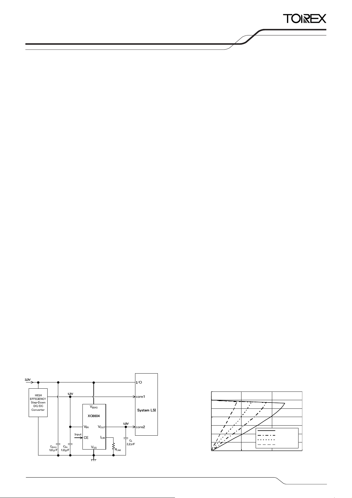
■TYPICAL APPLICATION CIRCUIT
pin.
LIM
). When the output current reaches the current limit, the output
L
pin quickly returns to the VSS level.
OUT
FEATURES
Maximum Output Current
ON Resistance
Bias Voltage Range
Input Voltage Range
Output Voltage Range
Output Voltage Accuracy
Ripple Rejection
Low Power Consumption
Stand-by Current
Under-voltage Lockout
Thermal Shutdown
Protection Circuit
Function
CE Pull-Down (Active High)
C
Operating Ambient Temperature
Output Capacitor
Packages
Environmentally Friendly
1A (1.3A Limit)
:
: 0.15Ω@V
: 2.5V~6.0V
: 0.5V~3.0V
: 0.5V~1.8V (0.1V increments)
: ±0.015V@V
±0.020V@V
: 60dB@f=1kHz (V
75dB@f=1kHz (V
: 100μA (V
: 0.01μA (V
1.8V (V
:
: 150℃@detect, 125℃@release
Foldback Current Limit, TSD, UVLO
:
Soft-start
:
High Speed Discharge
L
: -40℃~+85℃
: Ceramic Capacitor Compatible (2.2μF)
USP-6C, SOT-26W
:
EU RoHS Compliant, Pb Free
:
=3.6V, V
BIAS
<1.2V
OUT
≧1.2V
OUT
), 6.5μA (VIN)@V
BIAS
), 0.01μA (VIN)
BIAS
), 0.4V (VIN)
BIAS
OUT
BIAS_PSRR
IN_PSRR
■TYPICAL PERFORMANCE
CHARACTERISTICS
XC6604x121MR-G
1.4
1.2
(V)
OUT
1
0.8
0.6
0.4
0.2
Output Voltage: V
0
0.0 0.5 1.0 1.5
C
BIAS=CIN
Output Current: I
V
=3.6V, VIN=1.5V
BIAS=VCE
=1.0μF, CL=2.2μF, Ta=25℃
RLIM2=0kΩ
RLIM2=22kΩ
RLIM2=56kΩ
RLIM2=120kΩ
(A)
OUT
=1.2V
)
)
OUT
=1.2V
1/30
XC6604 Series
■BLOCK DIAGRAMS
Type A
Type B
■PRODUCT CLASSIFICATION
●Ordering Information
XC6604①②③④⑤⑥-⑦
DESIGNATOR ITEM SYMBOL DESCRIPTION
①
②③
④
⑤⑥-⑦
(*1)
The “-G” suffix denotes Halogen and Antimony free as well as being fully RoHS compliant.
(*1)
Output Voltage Accuracy 1
Packages (Order Unit)
Type
Output Voltage
●Selection Guide
TYPE SOFT-START
CURRENT
LIMITTER
THERMAL
SHUTDOWN
A Yes Adjustable Yes Yes Yes Yes
B No Adjustable Yes Yes Yes Yes
A
B
Refer to Selection Guide
05~18 e.g. 1.2V → ②=1, ③=2
±0.015V (V
<1.2V), ±0.020V (V
OUT
ER-G USP-6C (3,000/Reel)
MR-G SOT-26W (3,000/Reel)
UVLO
CE PULL-DOWN
RESISTOR
≧1.2V)
OUT
CL AUTO DISCHARGE
2/30
XC6604
Series
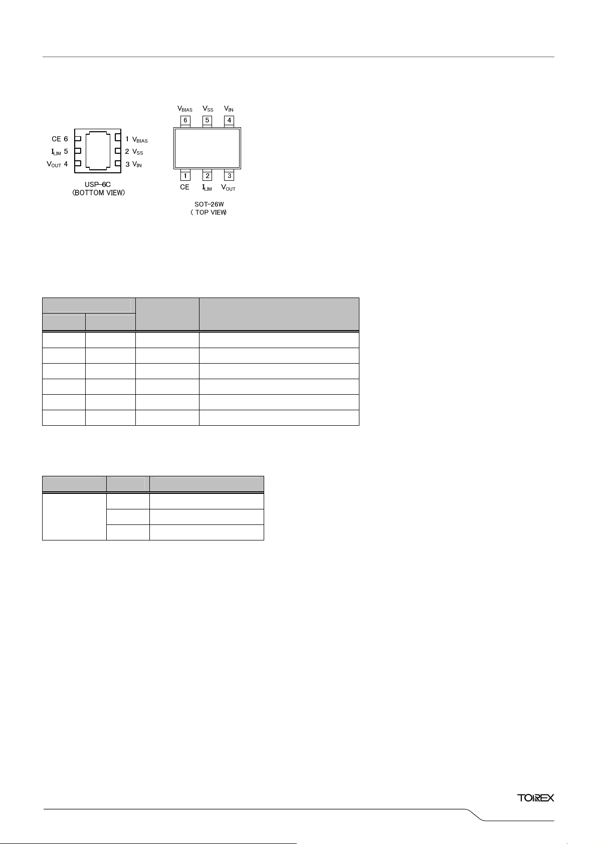
■PIN CONFIGURATION
*The dissipation pad for the USP-6C package should be solder-plated in recommended mount pattern and metal masking so as to enhance
mounting strength and heat release. If the pad needs to be connected to other pins, it should be connected to the V
(No. 2) pin.
SS
■PIN ASSIGNMENT
PIN NUMBER
PIN NAME FUNCTIONS
USP-6C SOT-26W
1 6 V
Power Supply Input
BIAS
2 5 VSS Ground
3 4 VIN Driver Transistor Input
4 3 V
5 2 I
Output
OUT
Current Limit Resistance Connection
LIM
6 1 CE ON/OFF Control
■FUNCTION CHART
PIN NAME SIGNAL STATUS
L Stand-by
CE
H Active
OPEN Stand-by
3/30
XC6604 Series
■ABSOLUTE MAXIMUM RATINGS
PARAMETER SYMBOL RATINGS UNITS
Ta =2 5℃
Bias Voltage V
Input Voltage VIN
Output Current I
Output Voltage
(*2)
V
CE Input Voltage VCE
I
Pin Voltage
LIM
(*3)
I
USP-6C
Power Dissipation
SOT-26W
Operating Ambient Temperature Topr
Storage Temperature Tstg
* All voltages are described based on the VSS pin.
(*1)
I
≦Pd/(VIN-V
OUT
(*2)
The maximum value should be either V
(*3)
The maximum value should be either VIN+0.3 or +6.5 in the lowest.
(*4)
The power dissipation measured with the test board condition is listed as reference data.
Please refer to page 26〜27 for details.
OUT
)
BIAS
BIAS
-0.3~+6.5
-0.3~+6.5
OUT
OUT
-0.3~V
-0.3~VIN+0.3 or +6.5
(*1)
1.65
+0.3 or +6.5
BIAS
-0.3~+6.5
LIM
Pd
-0.3~VIN+0.3 or +6.5
120
1000 (PCB mounted)
250
600 (PCB mounted)
-40~+85 ℃
-55~+125 ℃
+0.3, VIN+0.3 or +6.5 in the lowest.
(*4)
(*4)
V
V
A
V
V
V
mW
4/30
■ELECTRICAL CHARACTERISTICS
PARAMETER SYMBOL CONDITIONS MIN. TYP. MAX. UNITS CIRCUIT
Bias Voltage V
Input Voltage V
Output Voltage V
(*3
Maximum Output Current
)
I
Load Regulation ΔV
Dropout Voltage Vdif
Supply Current 1
(*6)
I
Supply Current 2 IIN I
Stand-by Current 1 I
Stand-by Current 2 I
Bias Line Regulation
Input Line Regulation
Bias UVLO Voltage V
Bias UVLO Release Voltage
Input UVLO Voltage VIN_
Input UVLO Release Voltage
Output Voltage
Temperature Characteristics
Bias Ripple Rejection R
atio V
Input Ripple Rejection Ratio
Current Limit
Adjustable Current
Limit Accuracy
(*3)
I
(*8)
Short - Circuit Current I
Thermal Shutdown
Detect Temperature
Thermal Shutdown
Release Temperature
Thermal Shutdown
Hysteresis Width
CL Auto-Discharge Resistance
CE "H" Level Voltage V
CE "L" Level Voltage V
CE "H" Level Current I
CE "L" Level Current I
Soft-Start Time
Output Rise Time
(*7)
(Type A) tSS
(*7)
(Type B) tON
Inrush Current (Type A) I
NOTE:
Unless otherwise stated, V
(*1)
V
= Effective output voltage
OUT(E)
(*2)
V
= Nominal output voltage
OUT(T)
(*3)
Mount conditions affect heat dissipation. Maximum output current is not guaranteed when TSD starts to operate earlier.
(*4)
Vdif={V
(*5)
Please refer to the table E-1 named DROPOUT VOLTAGE CHART
(*6)
Supply current 1 (I
(*7)
A time between the CE input goes over the CE H threshold and the output reaches VOUT(E)x0.9V.
(*8)
Design value
IN1-VOUT1
V
is an input voltage when V
IN1
V
is a voltage equal to 98% of the output voltage where V
OUT1
BIAS=VCE
}
) may be fluctuated because that some bias current flows into the output.
BIAS
2.5 - 6.0 V ①
BIAS
0.5 - 3.0 V ①
IN
V
<1.2V -0.015 +0.015
(*1)
I
OUT(E)
OUTMAX
1mA≦I
OUT
(*4)
I
I
BIAS
V
BIAS_STB
V
IN_STB
ΔV
/
OUT
(ΔV
・
V
BIAS
OUT
ΔV
/
OUT
(ΔVIN・
V
)
OUT
BIAS_UVLOD
V
BIAS_UVLOR
UVLOD
VIN_
UVLOR
ΔV
/
OUT
・
V
(ΔTopr
OUT
BIAS_PSRR
V
IN_PSRR
V
LIM
I
- (-35) - (35) %
LIM_ADJ
V
SHORT
T
Junction Temperature - 150 - ℃ ①
TSD
T
Junction Temperature - 125 - ℃ ①
TSR
T
TSD-TTSR
R
VCE=VSS, V
DCHG
0.65 - 6.00 V ④
CEH
V
CEL
V
CEH
V
CEL
RUSH
=3.6V, VIN=V
OUT1
=100mA
OUT
V
<1.2V, V
OUT(T)
V
≧1.2V, V
OUT(T)
OUT
=1A - E-1
OUT
=0A 76 100 143 μA ②
OUT
=0A
OUT
=6.0V, VIN=3.0V, VCE=VSS - 0.01 0.10 μA ②
BIAS
=6.0V, VIN=3.0V, VCE=VSS - 0.01 0.15 μA ②
BIAS
V
<
1.2V, VCE=V
OUT(T)
)
V
≧
1.2V, VCE=V
OUT(T)
V
+0.1V≦VIN≦3.0V - 0.01 0.10 %/V ①
OUT(T)
V
2.5 - 6.0 V ①
V
0.5 - 3.0 V ①
I
=100mA
OUT
)
-40℃≦Topr≦85℃
V
BIAS=VCE
I
=100mA, f=1kHz, C
OUT
VIN=V
OUT(T)
I
=100mA, f=1kHz, CIN=OPEN
OUT
={V
OUT
OUT=VSS
Junction Temperature - 25 - ℃ ①
BIAS=VCE
=6.0V, VCE=V
BIAS
V
=0V→3.6V, tr=5μs
CE
V
=0V→3.6V, tr=5μs
CE
C
=2.2μF
L
C
=10μF
L
+0.3V, I
OUT(T)
appears at the output during decreasing input voltage gradually.
OUT(T)
V
≧1.2V -0.020
OUT(T)
=2.5V
BIAS=VCE
BIAS=VCE=VOUT(T)
+1.3V
1.0 - - A ①
≦1A - 37 68 mV ①
V
<1.2V 0.1 - 8.7
OUT(T)
V
≧1.2V 3.9 - 14.2
OUT(T)
, 2.5V
≦V
≦
BIAS
≦V
BIAS
6.0V
≦
6.0V
- 0.01 0.10 %/V ①
- 1.28 V ①
SS
- 0.23 V ①
SS
BIAS
BIAS
, V
OUT(T)
+1.3V
V
OUT(T)
(*2)
+0.020
(*5)
mV ①
- ±30 - ppm/℃ ①
=3.6VDC+0.2V
+0.3VDC+0.2V
OUT@IOUT
=1A}×0.95 1.0 1.3 - A ①
p-pAC
BIAS
p-pAC
=OPEN
- 60 - dB ③
- 75 - dB ③
- 90 - mA ①
OUT=VOUT(T)
130 190 255 Ω ①
- 0.41 V ④
SS
=6.0V 3.2 6.0 10.6 μA ④
-0.1 - 0.1 μA ④
SS
225 430 600
- - 110
- - 70
- - 85
- - 155
- - 215
Pin=VSS
LIM
OUT(T)
+0.3V at I
=1A is input to the VIN pin.
OUT
=1mA , C
OUT
V
OUT(T)
V
OUT(T)
V
OUT(T)
V
OUT(T)
BIAS=CIN
BIAS=VCE
≦1.2V
>1.2V
≦1.2V
>1.2V
=1.0μF, CL=2.2μF, I
=3.6 and VIN=V
XC6604
Series
Ta =2 5 ℃
V ①
μA ②
①
μs ⑤
μs ⑤
mA
⑤
5/30
XC6604 Series
■ELECTRICAL CHARACTERISTICS (Continued)
●Dropout Voltage Chart
E-1
NOMINAL
OUTPUT
VOLTAGE
V
OUT(T)
0.5 2.5 152 218 2.8 3.1 3.7 4.5
0.6 2.4 2.7 3.0 3.6 4.4
0.7 2.3
0.8 2.2 158 228 2.5 152 218 2.8 3.4 4.2
0.9 2.1 162 233 2.4 2.7 3.3
1.0 2.0 165 238 2.3
1.1 1.9 167 243 2.2 158 228 2.5 152 218 3.1 3.9
1.2 1.8 169 253 2.1 162 233 2.4 3.0 3.8
1.3 1.7 179 268 2.0 165 238 2.3
1.4 1.6 189 283 1.9 167 243 2.2 158 228 2.8 3.6
1.5 1.5 202 303 1.8 169 253 2.1 162 233 2.7 3.5
1.6 1.4 213 328 1.7 179 268 2.0 165 238 2.6
1.7 1.3 225 373 1.6 189 283 1.9 167 243 2.5 152 218 3.3
1.8 1.2 255 423 1.5 202 303 1.8 169 253 2.4 155 223 3.2 146 213
* Dropout voltage is defined as the V
V
BIAS
VGS
(V)
TYP. MAX.
155 223
=3.0V V
Vdif(mV) Vdif(mV) Vdif(mV) Vdif(mV) Vdif(mV)
V
(V)
2.6
GS
=3.3V V
BIAS
GS
TYP. MAX.
146 213
155 223
(=V
BIAS–VOUT(E)
6/30
DROPOUT VOLTAGE (mV)
=3.6V V
BIAS
V
GS
(V)
TYP. MAX.
2.9 3.5 4.3
146 213
2.6
155 223
V
(V)
3.2 4.0
2.9 3.7
=4.2V V
BIAS
GS
TYP. MAX.
140 208
146 213
) of the driver transistor.
BIAS
VGS
(V)
TYP. MAX.
137 206
4.1
140 208
3.4
=5.0V
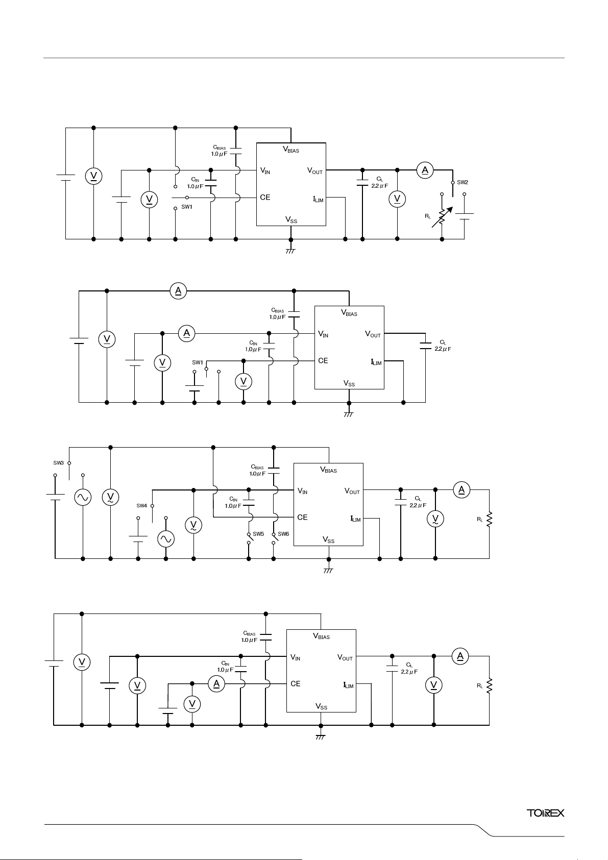
■TEST CIRCUITS
CIRCUIT①
CIRCUIT②
CIRCUIT③
CIRCUIT④
XC6604
Series
7/30

XC6604 Series
■TEST CIRCUITS (Continued)
CIRCUIT⑤
8/30
XC6604 Series, Type A
XC6604 Series, Type B
XC6604
Series
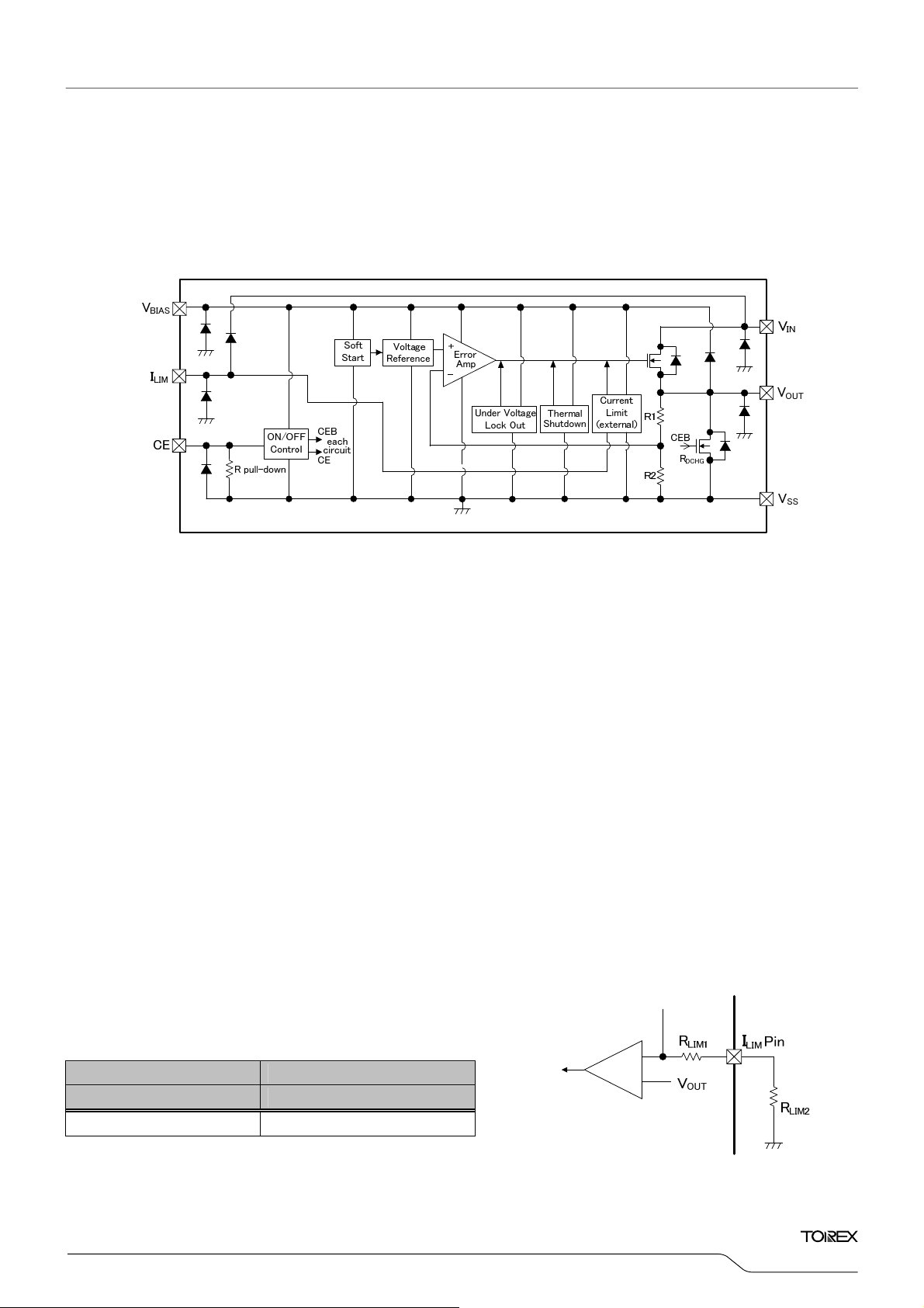
■OPERATIONAL DESCRIPTION
The voltage divided by resistors R1 and R2 is compared with the internal reference voltage by the error amplifier. The V
by the subsequent output signal. The output voltage at the V
V
pin is power supply pin for output voltage control circuit, protection circuit and CE circuit. Also, the V
BIAS
output current. V
pin is connected to a driver transistor and provides output current.
IN
In order to obtain high efficient output current through low on-resistance, please take enough V
pin is controlled and stabilized by a system of negative feedback.
OUT
pin supplies some current as
BIAS
(=V
BIAS
– V
GS
) of the driver transistor.
OUT(E)
Figure1: XC6604 Series, Type A
<Current Limiter, Short-Circuit Protection>
The XC6604 series includes a combination of a fixed current limiter circuit and a foldback short-circuit protection. When the output current
reaches the current limit, the output voltage drops and this operation makes the output current foldback to be decreased.
The current limit can be set freely with connecting a resistor to the I
LIM
pin.
Please note about the foldback circuit characteristics below;
●Output voltage may not rise when the output voltage is lower than 0V at the IC operation start.
●Current over the foldback current limit will not flow at the IC operation start.
●Please use type A (with soft-start time) to prevent from inrush current, because the circuit may not response to a drastic current change such
as the inrush current.
When the I
pin is left open, driver transistor will be forced off.
LIM
Current Limit is calculated by the following formulas.
= V
I
LIM
/ ( R
+ R
OUT(T
= V
R
LIM1
)
OUT(T
LIM1
)
) × 79645.7 [A]
LIM2
/ ( 16.3 × 10⁻⁶ ) [Ω]
: Current Limit
I
LIM
: Nominal Output Voltage
V
OUT(T)
: Internal Current Limit Resistance
R
LIM1
: External Current Limit Resistance
R
LIM2
Figure 2: XC6604 Series, Range of adjustable current limit
OUTPUT VOLTAGE RANGE ADJUSTABLE CURRENT LIMIT
V
I
OUT(T)
LIM
0.5V~1.8V 0.5A~1.3A
XC6604 Series, R
LIM2
pin is then driven
OUT
Connecting
9/30
 Loading...