

XC6501
ETR03037-007
200mA High Speed LDO Regulator, Output Capacitor-Less, Low Power Consumption
■GENERAL DESCRIPTION
The XC6501 series is a high speed, low noise CMOS LDO regulator that can provide stable output voltages even without a load
capacitor C
externally. The series consists of a reference voltage source, driver transistor, error amplifier, current limit circuit, and phase
compensation circuit.
The CE function enables the circuit to be put into stand-by mode by inputting a low level signal to the CE pin thereby reducing
current consumption from an already low 13μA (in operation) to less than 0.1μA. In the stand-by mode, if a C
the electric charge stored at CL can be discharged via the internal auto-discharge switch and as a result, the V
returns to the V
The current limit fold-back circuit operates as a short circuit protection and a current limiter function for the output pin.
■APPLICATIONS
●Mobile phones (RF, NFC, I/O etc.)
●Portable games
●Camera modules
●Wireless LAN modules
●LCD modules
●Bluetooth
●Digital-TV tuners
. This is possible because phase compensation is carried out internally unlike other LDOs where it is done
L
capacitor is used,
L
pin quickly
OUT
level.
SS
■FEATURES
:
Maximum Output Current
Operating Voltage Range
Output Voltage Range
Output Voltage Accuracy
Dropout Voltage
Low Power Supply
Stand-by Current
Ripple Rejection
Protection Circuits
Output capacitor is not required
C
High Speed Auto Discharge
L
Operating Ambient Temperature
Packages
Environmentally Friendly
200mA
:
1.4~6.0V
:
1.2~5.0V
:
±1% or ±0.02V
:
150mV@I
:
13μA @V
:
Less than 0.1μA
:
50dB@f=1kHz,V
:
Current limit (300mA, TYP.)
Short circuit protection
:
Internal phase compensation
:
-40℃~+85℃
:
SOT-25, SSOT-24, USP-4,
USPN-4,USP-3
:
EU RoHS Compliant, Pb Free
=100mA, V
OUT
=2.8V
OUT
OUT
=2.8V
OUT
=2.8V
■
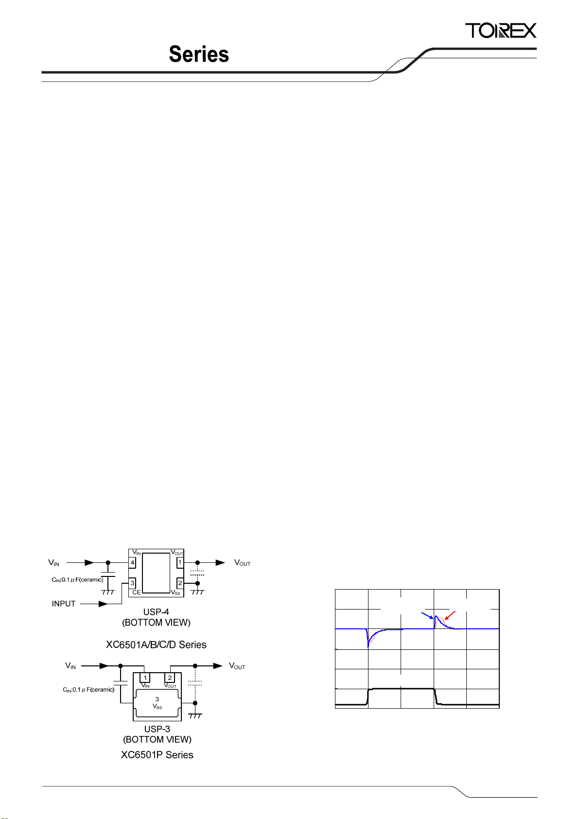
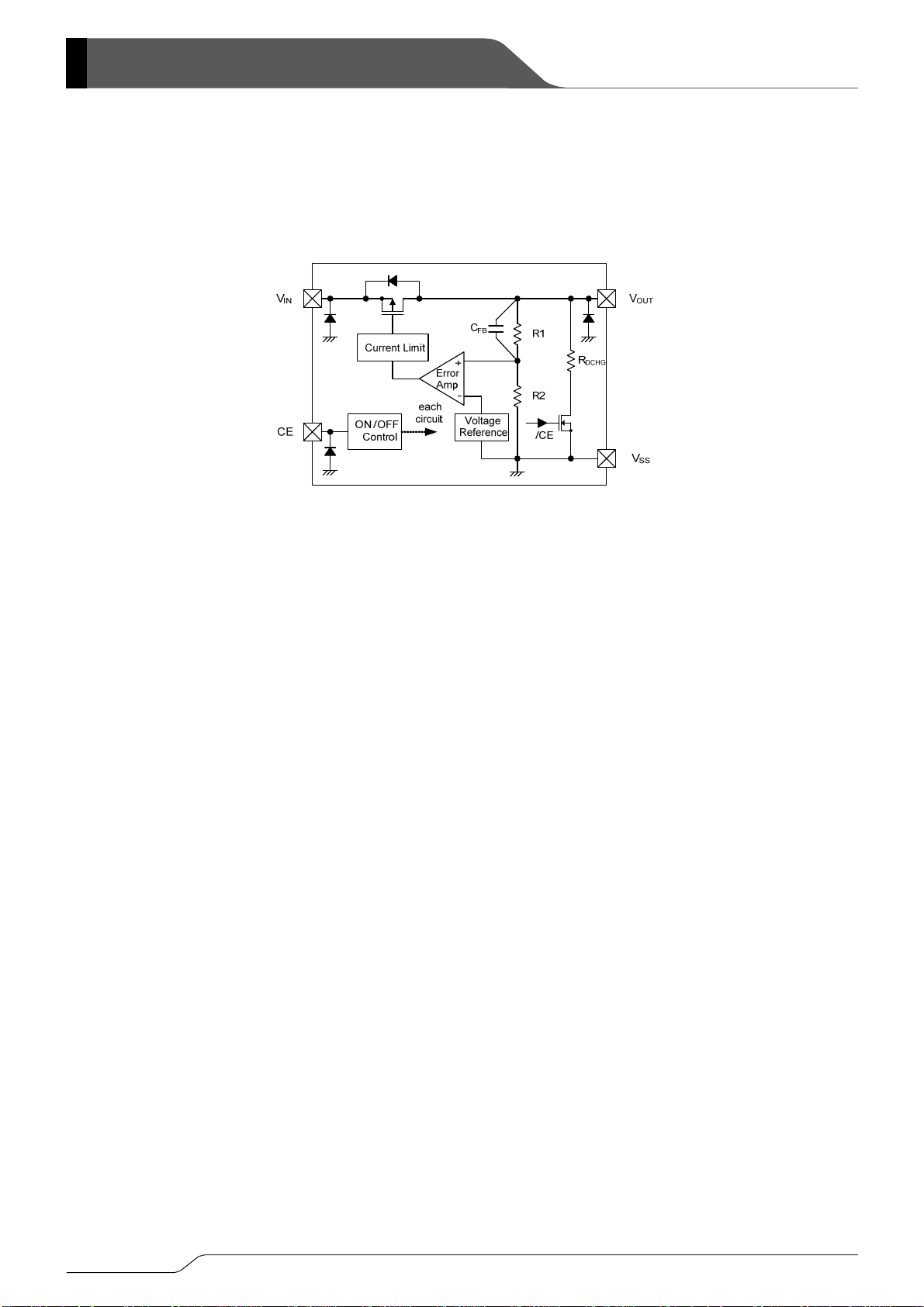
TYPICAL APPLICATION CIRCUIT
■TYPICAL PERFORMANCE
CHARACTERISTICS
3.2
3.2
3.0
3.0
(V)
(V)
OUT
OUT
2.8
2.8
2.6
2.6
2.4
2.4
2.2
2.2
Output Voltage: V
Output Voltage: V
2.0
2.0
XC6501 Series
XC6501 Series
Without CL
C
C
し
し
無
無
L
L
Output Current
Output Current
Time (40μs/div)
Time (40μs/div)
Ta= 25℃,tr=tf=5μs
Ta= 25℃,tr=tf=5μs
C
C
=0.1μF (ceramic)
=0.1μF (ceramic)
IN
IN
CL=1.0μF
CL=1.0μF
300
300
250
250
200
200
150
150
100
100
50
50
0
0
1/23
(mA)
(mA)
OUT
OUT
Output Current: I
Output Current: I
XC6501 Series
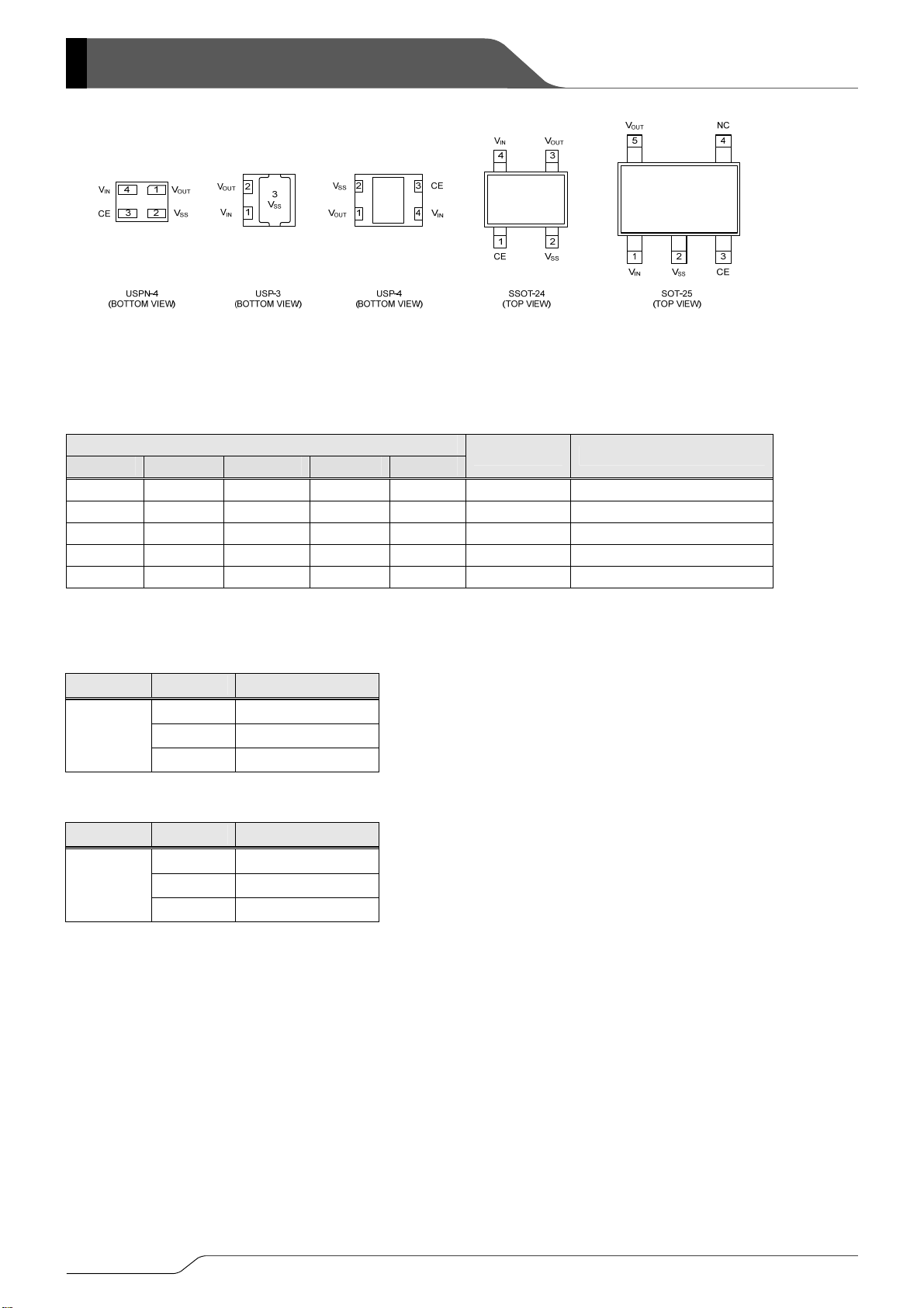
■PIN CONFIGURATION
*The heat dissipation pad of the USP-4 package is reference to solder as the reference
mount pattern and metal mask pattern for mounting strength. The mount pattern should
be electrically opened or connected to the V
■PIN ASSIGNMENT
PIN NUMBER
USP-3 USP-4 SSOT-24 SOT-25 USPN-4
1 4 4 1 4 VIN Power Supply Input
2 1 3 5 1 V
3 2 2 2 2 VSS Ground
- 3 1 3 3 CE ON/OFF Control
- - - 4 - NC No Connection
(No.2) pin.
SS
PIN NAME FUNCTIONS
Output
OUT
■FUNCTION CHART
1)XC6501 series A/B type
PIN NAME SIGNAL STATUS
L OFF
CE
2)XC6501 series C/D type
PIN NAME SIGNAL STATUS
CE
H ON
OPEN Undefined
L OFF
H ON
OPEN OFF
2/31
■PRODUCT CLASSIFICATION
●Ordering Information
XC6501①②③④⑤⑥-⑦
DESIGNATOR ITEM SYMBOL DESCRIPTION
①
②③
④
⑤⑥-⑦
(*1)
The “-G” suffix denotes Halogen and Antimony free as well as being fully RoHS compliant.
(*2)
USP-3 is available only for XC6501P series.
(*1)
(*1)
Regulator Type
Output Voltage
Output Voltage Type
[Accuracy]
Packages
(Order Unit)
A CE High Active, Without CE Pull-down, Without CL discharge
B CE High Active, Without CE Pull-down, With CL discharge
C CE High Active, With CE Pull-down, Without CL discharge
D CE High Active, With CE Pull-down, With CL discharge
P 3 pin, without CE pin (USP-3)
12~50 ex.)28V → ②=2, ③=8
1
A
HR USP-3
HR-G USP-3
0.1V increments ex.)1.80V → ②=1, ③=8, ④=1
[±0.02V @ 1.2V~1.9V, ±1% @ 2.0V~5.0V]
0.05V increments ex.)1.85V → ②=1, ③=8, ④=A
[±0.02V @ 1.25V~1.95V, ±1% @ 2.05V~4.95V]
(*2)
(3,000/Reel)
(*2)
(3,000/Reel)
GR USP-4 (3,000/Reel)
GR-G USP-4 (3,000/Reel)
NR SSOT-24 (3,000/Reel)
NR-G SSOT-24 (3,000/Reel)
MR SOT-25 (3,000/Reel)
MR-G SOT-25 (3,000/Reel)
7R-G USPN-4
(5,000/Reel)
XC6501
Series
3/31
XC6501 Series
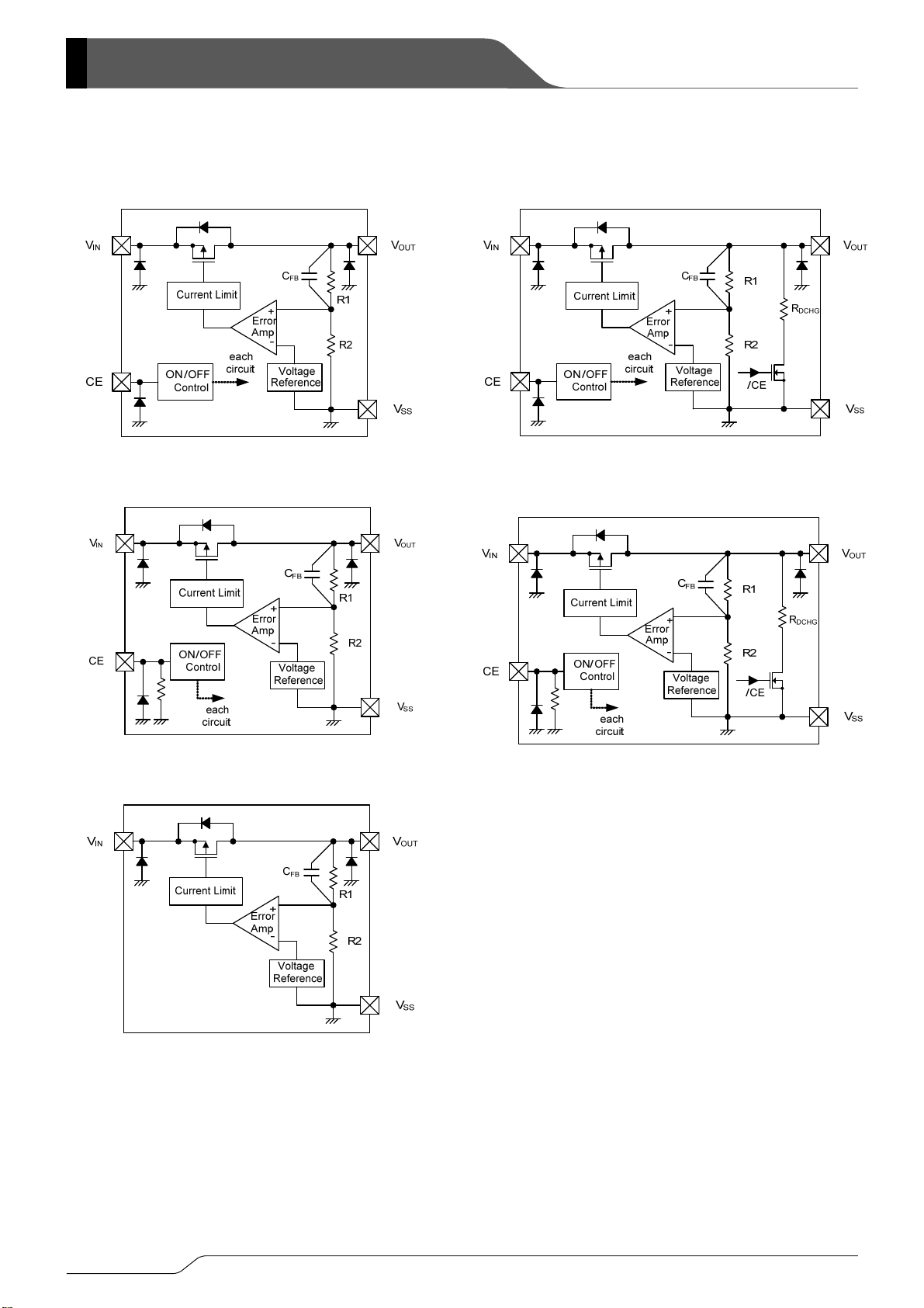
■BLOCK DIAGRAMS
1) XC6501 Series A type
3) XC6501 Series C type
2) XC6501 Series B type
4) XC6501 Series D type
5) XC6501 Series P type
*Diodes inside the circuit are an ESD protection diode and a parasitic diode.
*図のダイオードは、静電保護用のダイオードと寄生ダイオードです。
4/31
■ ABSOLUTE MAXIMUM RATINGS
PAR AMETER SYMBOL RATINGS UNITS
Input Voltage VIN -0.3~+6.5 V
Output Current I
Output Voltage V
400
OUT
-0.3~VIN+0.3 or +6.5
OUT
CE Input Voltage VCE -0.3~+6.5 V
Power Dissipation
USPN-4
USP-3
USP-4
SSOT-24
SOT-25
Pd
600 (PCB mounted)
1000 (PCB mounted)
1000 (PCB mounted)
500 (PCB mounted)
600 (PCB mounted)
Operating Ambient Temperature Topr -40~+85 ℃
Storage Temperature Tst g -5 5~+125 ℃
* All voltages are described based on the VSS pin.
(*1) I
≦Pd/(VIN-V
OUT
(*2) The maximum value should be V
(*3) The power dissipation figure shown is PCB mounted and is for reference only. Please refer to page 24~28 for details.
OUT
)
+0.3 or +6.5 in the lowest.
IN
(*1)
mA
100
(*3)
(*2)
V
120
(*3)
120
150
(*3)
(*3)
mW
250
(*3)
XC6501
Series
5/31

XC6501 Series
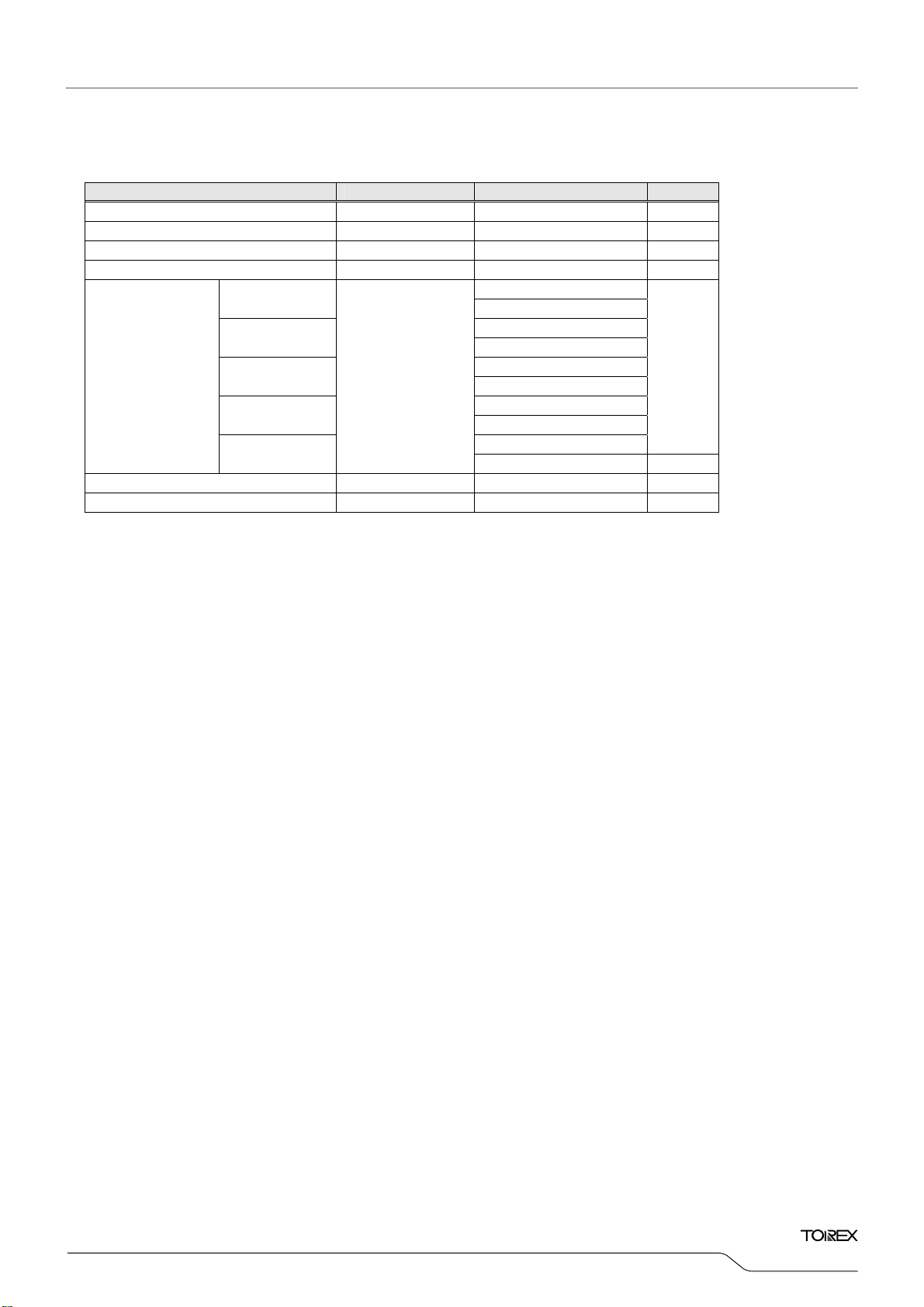
■ELECTRICAL CHARACTERISTICS
●XC6501 Series A/B/C/D Type
PAR AMETER SYMBOL CONDITIONS MIN. TYP. MAX. UNITS
(*2)
Output Voltage V
Maximum Output
Current
OUT(E)
I
OUTMAX
Load Regulation ΔV
(*4)
Dropout Voltage
Supply Current I
Stand-by
Current
Line Regulation
(ΔV
I
ΔV
IN・VOUT
Input Voltage V
Output Voltage
Temperature
Characteristics
Rejection Ratio
ΔV
(ΔTopr・V
PSRR
Current Limit I
Short - Circuit
Current
CE High Level
Voltage
CE Low Level
Voltage
Current
I
SHORT
V
V
CE Low Level
Current
CL
Auto-Discharge
(*7)
Resistance
R
V
V
(*1)
V
V
VCE=VIN 200 - - mA ①
VCE=VIN、0.1mA≦I
OUT
Vdif VCE=VIN、I
V
SS
V
STBY
V
/
OUT
)
V
1.4 - 6.0 V ①
IN
V
/
OUT
)
-40℃≦To pr ≦85℃
OUT
V
V
V
V
V
V
V
LIM
V
level
1.0 - 6.0 V ①
CEH
VSS - 0.25 V ①
CEL
I
V
CEH
I
V
CEL
VIN=6.0V、V
DCHG
V
≦1.95V
OUT(T)
CE=VIN、IOUT
OUT(T)
CE=VIN、IOUT
IN=VCE
=6.0V、VCE=VSS - 0.01 0.1 μA ②
IN
OUT(T)
CE=VIN、IOUT
CE=VIN、IOUT
OUT(T)
={V
IN
CE=VIN、IOUT
OUT(T)
=5.75VDC+0.5Vp-pAC
IN
CE=VIN、IOUT
CE=VIN
CE=VIN、VOUT
CE=VIN
CE=VIN
=6.0V、V
IN
=10mA
≧2.0V
=10mA
≦100mA - 15 45 mV ①
OUT
=100mA - E-1
OUT
=6.0V、I
=0mA E-2
OUT
+0.5V≦VIN≦6.0V、
=30mA
=30mA
≦4.75V
+1.0}VDC+0.5Vp-pAC
OUT(T)
=30mA、f=1kHz Power Supply
≧4.80V
=30mA、f=1kHz
210 300 - mA ①
is short-circuited at the VSS
=6.0V
XC6501A/B -0.1 - 0.1 CE High Level
XC6501C/D 3.5 6.0 10
-0.1 - 0.1 μA ①
=1.2V、VCE=VSS - 250 300 Ω
OUT
=5.0V、VCE=VSS - 400 480 Ω
OUT
-0.02
×0.99
(*3)
(*3)
V
OUT(T
)
(*6)
μA ②
(*3)
+0.02
(*3)
×1.01
(*5)
mV ①
- 0.10 0.20 %/V ①
- ±100 - ppm/℃ ①
- 50 - dB ③
- 25 - mA ①
Ta =2 5℃
CIRCUIT
V ①
μA ①
①
Notes:
Unless otherwise stated regarding input voltage conditions, V
*1: V
*2: V
*3: MIN and MAX values of V
*4: Vdif={V
: An actual output voltage when an amply stabilized(V
OUT(E)
: Nominal output voltage value
OUT(T)
are shown in the voltage table “E-0”.
OUT(E)
– V
OUT1
}
appears as input voltage is gradually decreased.
OUT1
IN1
: The input voltage when V
V
IN1
V
: A voltage equal to 98% of the output voltage when an amply stabilized I
OUT1
IN=VOUT(T)
(*2)
+1.0V.
+1.0V) is supplied with constant I
OUT(T)
OUT (VOUT(T)
*5: Please refer to page E-1.
*6: Please refer to page E-2.
*7: This function is built in the XC6501B/D series only.
The XC6501A/C series discharges by only R1+ R2 resistors as shown in the block diagrams.
6/31
.
OUT
+1.0V) is input.
XC6501
Series
■ELECTRICAL CHARACTERISTICS (Continued)
●XC6501 Series P Type
PARAMETER SYMBOL CONDITIONS MIN. TYP. MAX. UNITS CIRCUIT
}
V
I
ΔV
(ΔVIN・
(
ΔTopr・V
PSRR
Output Voltage
Maximum Output
Current
Output Voltage
Dropout Voltage
(*4)
Supply Current
Line Regulation
Input Voltage
Output Voltage
Temperature
Characteristics
Power Supply
Rejection Ratio
Current Limit
Short Circuit
Current
Notes:
Unless otherwise stated regarding input voltage conditions, V
*1: V
*2: V
*3: MIN and MAX values of V
*4: Vdif={V
*5: Please refer to page E-1.
*6: Please refer to page E-2.
: An actual output voltage when an amply stabilized(V
OUT(E)
: Nominal output voltage value
OUT(T)
– V
IN1
OUT1
V
: The input voltage when V
IN1
V
: A voltage equal to 98% of the output voltage when an amply stabilized I
OUT1
(*2)
V
OUT(E)
V
I
(*1)
I
200 - - mA
OUTMAX
ΔV
OUT
/
)
0.1mA≦I
VIN=6.0V、I
V
I
OUT
V
I
dif
ISS
OUT
V
≦1.95V
OUT(T)
=10mA
OUT
≧2.0V
OUT(T)
=10mA
OUT
≦100mA
OUT
=100mA - E-1
OUT
=0mA
OUT
+0.5V≦VIN≦6.0V、
OUT(T)
=30mA
OUT
(*3)
-0.02
V
(*3)
×0.99
- 15 45 mV
E-2
- 0.10 0.20 %/V
OUT(T)
(*6)
+0.02
×1.01
(*5)
mV
(*3)
(*3)
VIN 1.4 - 6.0 V
ΔV
/
I
OUT
OUT
)
=30mA
OUT
-40℃≦Topr≦85℃
V
≦4.75V
OUT(T)
VIN={V
OUT(T)
I
=30mA、f=1kHz
OUT
V
≧4.80V
OUT(T)
- ±100 - ppm
+1.0}VDC+0.5Vp-pAC
- 50 - dB
VIN=5.75VDC+0.5Vp-pAC
I
=30mA、f=1kHz
OUT
I
210 300 - mA
LIM
I
V
SHORT
are shown in the voltage table “E-0”.
OUT(E)
OUT1
is short-circuited at the VSS level - 25 - mA
OUT
(*2)
IN=VOUT(T)
OUT(T)
+1.0V.
+1.0V) is supplied with constant I
OUT
.
appears as input voltage is gradually decreased.
OUT (VOUT(T)
+1.0V) is input.
Ta =2 5℃
V
μA ②
①
①
①
①
①
①
①
③
①
①
7/31
XC6501 Series
■ELECTRICAL CHARACTERISTICS (Continued)
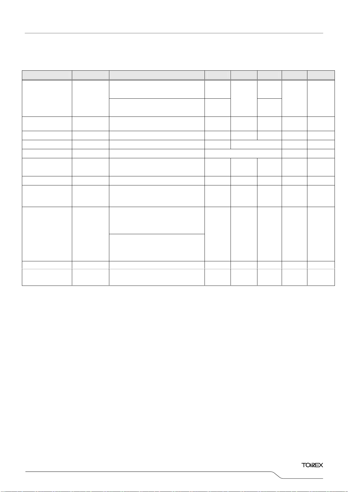
●Voltage Chart
18
19
20
E-0 E-1 E-2
NOMINAL
VOLTAGE
(V)
V
OUT(T)
1.20 1.1800 1.2200
1.25 1.2300 1.2700
1.30 1.2800 1.3200
1.35 1.3300 1.3700
1.40 1.3800 1.4200
1.45 1.4300 1.4700
1.50 1.4800 1.5200
1.55 1.5300 1.5700
1.60 1.5800 1.6200
1.65 1.6300 1.6700
1.70 1.6800 1.7200
1.75 1.7300 1.7700
1.80 1.7800 1.8200
1.85 1.8300 1.8700
1.90 1.8800 1.9200
1.95 1.9300 1.9700
2.00 1.9800 2.0200
2.05 2.0295 2.0705
2.10 2.0790 2.1210
2.15 2.1285 2.1715
2.20 2.1780 2.2220
2.25 2.2275 2.2725
2.30 2.2770 2.3230
2.35 2.3265 2.3735
2.40 2.3760 2.4240
2.45 2.4255 2.4745
2.50 2.4750 2.5250
2.55 2.5245 2.5755
2.60 2.5740 2.6260
2.65 2.6235 2.6765
2.70 2.6730 2.7270
2.75 2.7225 2.7775
2.80 2.7720 2.8280
2.85 2.8215 2.8785
2.90 2.8710 2.9290
2.95 2.9205 2.9795
3.00 2.9700 3.0300
3.05 3.0195 3.0805
OUTPUT
VOLTAGE
(V) (mV)
V
OUT(E)
MIN. MAX. TYP. MAX. MIN. TYP. MAX.
V
DROPOUT
VOLTAGE
ISS
dif
440 690
300 610
260 530
230 470
200 430
190 410
210 380
150 360
SUPPLY
CURRENT
(μA)
11 17
5
12
6
13
7 14
8/31
■ELECTRICAL CHARACTERISTICS (Continued)
●Voltage Table (continued)
E-0 E-1 E-2
XC6501
Series
NOMINAL
VOLTAGE
(V)
V
OUT(T)
3.10 3.0690 3.1310
3.15 3.1190 3.1820
3.20 3.1680 3.2320
3.25 3.2175 3.2825
3.30 3.2670 3.3330
3.35 3.3165 3.3835
3.40 3.3660 3.4340
3.45 3.4155 3.4845
3.50 3.4650 3.5350
3.55 3.5145 3.5855
3.60 3.5640 3.6360
3.65 3.6135 3.6865
3.70 3.6630 3.7370
3.75 3.7125 3.7875
3.80 3.7620 3.8380
3.85 3.8115 3.8885
3.90 3.8610 3.9390
3.95 3.9105 3.9895
4.00 3.9600 4.0400
4.05 4.0095 4.0905
4.10 4.0590 4.1410
4.15 4.1085 4.1915
4.20 4.1580 4.2420
4.25 4.2075 4.2925
4.30 4.2570 4.3430
4.35 4.3065 4.3935
4.40 4.3560 4.4440
4.45 4.4055 4.4945
4.50 4.4550 4.5450
4.55 4.5045 4.5955
4.60 4.5540 4.6460
4.65 4.6035 4.6965
4.70 4.6530 4.7470
4.75 4.7025 4.7975
4.80 4.7520 4.8480
4.85 4.8015 4.8985
4.90 4.8510 4.9490
4.95 4.9005 4.9995
5.00 4.9500 5.0500
OUTPUT
VOLTAGE
(V) (mV)
V
OUT(E)
MIN. MAX. TYP. MAX. MIN. TYP. MAX.
DROPOUT
VOLTAGE
V
150 360
140 350
130 340
120 330 8 16
SUPPLY
CURRENT
ISS
dif
7
(μA)
14
21
15
22
23
9/31
XC6501 Series
■OPERATIONAL EXPLANATION
The voltage divided by resistors R1 & R2 is compared with the internal reference voltage by the error amplifier. The P-channel
MOSFET which is connected to the V
is controlled & stabilized by a system of negative feedback. The current limit circuit and short protect circuit operate in relation
to the level of output current. Further, the IC's internal circuitry can be shutdown via the CE pin's signal.
<CL High Speed Auto-Discharge Function>
The XC6501B/D series can discharge the electric charge in the output capacitor C
enables a whole IC circuit turn off, is inputted via the N-channel transistor located between the V
shown in the BLOCK DIAGRAM. The CL auto-discharge resistance value is set at 400Ω(V
The discharge time of the output capacitor C
setting time constant of a C
auto-discharge resistance value R
L
the output voltage after discharge via the N-channel transistor is calculated by the following formulas.
<Current Limiter, Short-Circuit Protection>
The XC6501 series’ fold-back circuit operates as an output current limiter and a short protection of the output pin. When the
load current reaches the current limit level, the fixed current limiter circuit operates and output voltage drops. When the
output voltage is shorted to the V
SS
<CE Pin>
The IC's internal circuitry can be shutdown via the signal from the CE pin with the XC6501 series. In shutdown mode output at
the V
pin will be pulled down to the VSS level via R1 & R2. However, as for the XC6501B/D series, the C
OUT
resistor is connected in parallel to R1 and R2 while the power supply is applied to the V
reaches the V
level becomes short. The output voltage becomes unstable, when the CE pin is open. If this IC is used with
SS
the correct output voltage for the CE pin, the logic is fixed and the IC will operate normally. However, supply current may
increase as a result of through current in the IC's internal circuitry when medium voltage is input.
pin is then driven by the subsequent output signal. The output voltage at the V
OUT
XC6501 Series B Type
, when a low signal to the CE pin, which
L
pin and the V
OUT
=5.0V @ VIN=6.0V at typical).
OUT
is set by the CL auto-discharge resistance R and the output capacitor CL. By
L
and an output capacitor value CL as τ (τ=C x R
DCHG
-t/
V= V
OUT(E)
or an expanded formula is
t=τ×ln(V
×e
OUT(E)
τ
/V)
V : Output voltage after discharge
V
: Output voltage
OUT(E)
t : Discharge time
τ:R
DCHG×CL
R
DCHG:CL
C
:Output capacitor
L
auto-discharge resistance
, its current flow reached and minimized to about 25mA.
pin. Therefore, time until the V
IN
pin as
SS
DCHG
auto-discharge
L
OUT
OUT
),
pin
pin
10/31

■NOTES ON USE
. Please use this IC within the stated absolute maximum ratings. The IC is liable to malfunction should the ratings be
1
exceeded.
2. This IC achieves stable operation without an output capacitor C
impedance is high, operations may become unstable due to noise and/or phase lag depending on output current.
Please wire the input capacitor C
3. Torex places an importance on improving our products and their reliability.
We request that users incorporate fail-safe designs and post-aging protection treatment when using Torex products
in their systems.
and the output capacitor CL as close to the IC as possible.
IN
by internal phase compensation. However, wiring
L
XC6501
Series
11/31

XC6501 Series
■TEST CIRCUITS
●Circuit ①
●Circuit ②
●Circuit ③
The CE pin does not exist in the XC6501 series P type, please disregard CE description in above test circuit.
●測定回路①
V
●測定回路②
●測定回路③
CIN=0.1μF
(ceramic)
V
V
V
IN
CE
A
V
A
CE
CE
V
OUT
V
SS
V
IN
V
OUT
V
SS
V
IN
V
OUT
V
SS
I
OUT
A
V
I
OUT
A
V
12/31

■TYPICAL PERFORMANCE CHARACTERISTICS
*CE Voltage condition: Unless otherwise stated, VCE =VIN
(1) Output Voltage vs. Output Current
1.5
XC6501x121
C
= 0.1μF (ceramic)
IN
V
= 2.2V
IN
1.5
XC6501x121
C
Ta = 25℃
= 0.1μF (ceramic)
IN
XC6501
Series
1.2
[V]
OUT
0.9
0.6
0.3
Output Voltage: V
0.0
0 50 100 150 200 250 300 350 400
Output Current: I
OUT
[mA]
XC6501x281
C
= 0.1μF (ceramic)
OUT
IN
[mA]
3.0
2.5
[V]
OUT
2.0
1.5
1.0
0.5
Output Voltage: V
0.0
0 50 100 150 200 250 300 350 400
Output Current: I
Ta = -40℃
Ta = 25℃
Ta = 85℃
V
IN
Ta = -40℃
Ta = 25℃
Ta = 85℃
= 3.8V
1.2
[V]
OUT
0.9
0.6
0.3
Output Voltage: V
0.0
0 50 100 150 200 250 300 350 400
Output Current: I
OUT
[mA]
XC6501x281
C
= 0.1μF (ceramic)
OUT
IN
[mA]
3.0
2.5
[V]
OUT
2.0
1.5
1.0
0.5
Output Voltage: V
0.0
0 50 100 150 200 250 300 350 400
Output Current: I
VIN = 1.5V
V
= 1.7V
IN
V
= 2.2V
IN
Ta = 25℃
VIN = 3.1V
V
= 3.3V
IN
V
= 3.8V
IN
XC6501x501
C
= 0.1μF (ceramic)
OUT
IN
[mA]
6.0
5.0
[V]
OUT
4.0
3.0
2.0
1.0
Output Voltage: V
0.0
0 50 100 150 200 250 300 350 400
Output Current: I
V
IN
Ta = -40℃
Ta = 25℃
Ta = 85℃
= 6.0V
XC6501x501
C
= 0.1μF (ceramic)
OUT
IN
[mA]
6.0
5.0
[V]
OUT
4.0
3.0
2.0
1.0
Output Voltage: V
0.0
0 50 100 150 200 250 300 350 400
Output Current: I
Ta = 25℃
VIN = 5.3V
V
= 5.5V
IN
= 6.0V
V
IN
13/31

XC6501 Series
■TYPICAL PERFORMANCE CHARACTERISTICS (Continued)
(2) Output Voltage vs. Input Voltage
XC6501x121
CIN = 0.1μF (ceramic)
1.4
XC6501x121
C
Ta = 25℃
= 0.1μF (ceramic)
IN
1.26
Ta = 25℃
1.2
[V]
OUT
1.0
0.8
I
OUT
I
0.6
Output Voltage: V
OUT
I
OUT
0.4
0.5 1.0 1.5 2.0 2.5
Input Voltage: V
[V]
IN
XC6501x281
3.0
2.8
[V]
OUT
2.6
2.4
2.2
Output Voltage: V
2.0
2.0 2.5 3.0 3.5 4.0
Input Voltage: V
CIN = 0.1μF (ceramic)
I
= 10mA
OUT
I
= 30mA
OUT
I
= 100mA
OUT
[V]
IN
= 10mA
= 30mA
= 100mA
Ta = 25℃
1.24
[V]
OUT
1.22
1.20
Output Voltage: V
1.18
1.16
I
OUT
I
OUT
I
OUT
1.14
2.0 3.0 4.0 5.0 6.0
Input Voltage: V
IN
[V]
XC6501x281
C
2.86
2.84
[V]
OUT
2.82
2.80
2.78
2.76
Output Voltage: V
2.74
3.2 3.9 4.6 5.3 6.0
Input Voltage: V
IN
I
OUT
I
OUT
I
OUT
[V]
IN
= 10mA
= 30mA
= 100mA
Ta = 25℃
= 0.1μF (ceramic)
= 10mA
= 30mA
= 100mA
14/31
XC6501x501
C
= 0.1μF (ceramic)
5.2
5.0
[V]
OUT
4.8
4.6
4.4
Output Voltage: V
4.2
4.0 4.5 5.0 5.5 6.0
Input Voltage: V
IN
I
OUT
I
OUT
I
OUT
IN
= 10mA
= 30mA
= 100mA
[V]
Ta = 25℃
XC6501x501
5.06
5.04
[V]
OUT
5.02
5.00
4.98
4.96
Output Voltage: V
4.94
5.2 5.4 5.6 5.8 6.0
Input Voltage: V
CIN = 0.1μF (ceramic)
I
OUT
I
OUT
I
OUT
[V]
IN
Ta = 25℃
= 10mA
= 30mA
= 100mA

XC6501
Series
■TYPICAL PERFORMANCE CHARACTERISTICS (Continued)
(3) Dropout Voltage vs. Output Current
XC6501x121
1.0
Ta = -40℃
0.8
Ta = 25℃
Ta = 85℃
0.6
0.4
0.2
Dropout Voltage: Vdif [V]
※Below the minimum operating voltage
0.0
0 50 100 150 200
Output Current: I
CIN = 0.1μF (ceramic) CIN = 0.1μF (ceramic)
[mA]
OUT
XC6501x501
C
= 0.1μF (ceramic)
OUT
IN
[mA]
0.5
Ta = -40℃
0.4
0.3
Ta = 25℃
Ta = 85℃
0.2
0.1
Dropout Voltage: Vdif [V]
0.0
0 50 100 150 200
Output Current: I
0.5
0.4
0.3
0.2
0.1
Dropout Voltage: Vdif [V]
0.0
0 50 100 150 200
(4) Supply Current vs. Input Voltage
16.0
12.0
[μA]
SS
8.0
4.0
Supply Current: I
0.0
0123456
XC6501x281
Ta = -40℃
Ta = 25℃
Ta = 85℃
Output Current: I
XC6501x121
Input Voltage: V
OUT
IN
[mA]
[V]
Ta = -40℃
Ta = 25℃
Ta = 85℃
XC6501x281
16.0
12.0
[μA]
SS
8.0
4.0
Supply Current: I
0.0
0123456
Input Voltage: V
[V]
IN
Ta = -40℃
Ta = 25℃
Ta = 85℃
XC6501x501
20.0
15.0
[μA]
SS
10.0
5.0
Supply Current: I
0.0
0123456
Input Voltage: V
IN
[V]
Ta = -40℃
Ta = 25℃
Ta = 85℃
15/31

XC6501 Series
■TYPICAL PERFORMANCE CHARACTERISTICS (Continued)
(5) Output Voltage vs. Ambient Temperature
[V]
OUT
1.24
1.22
XC6501x121
I
= 10mA
OUT
I
= 30mA
OUT
I
= 100mA
OUT
V
= 0.1μF (ceramic)
C
IN
= 2.2V
IN
[V]
OUT
2.90
2.85
XC6501x281
I
= 10mA
OUT
I
= 30mA
OUT
I
= 100mA
OUT
= 0.1μF (ceramic)
C
IN
VIN = 3.8V
1.20
1.18
Output Voltage: V
1.16
-50 -25 0 25 50 75 100
Ambient Temperature: Ta [℃]
XC6501x501
C
= 0.1μF (ceramic)
IN
[V]
OUT
5.10
5.05
I
OUT
I
OUT
I
OUT
= 10mA
= 30mA
= 100mA
5.00
4.95
Output Voltage: V
4.90
-50 -25 0 25 50 75 100
Ambient Temperature: Ta [℃]
V
= 6.0V
IN
2.80
2.75
Output Voltage: V
2.70
-50 -25 0 25 50 75 100
Ambient Temperature: Ta [℃]
(6) Supply Current vs. Ambient Temperature
XC6501
= V
+ 1.0V
V
IN
I
OUT
I
OUT
I
OUT
OUT
= 10mA
= 30mA
= 100mA
20.0
15.0
[μA]
SS
10.0
5.0
Supply Current: I
0.0
-50 -25 0 25 50 75 100
Ambient Temperature: Ta [℃]
(7) CE Threshold Voltage vs. Ambient Temperature
XC6501
I
= 1mA, CIN = 0.1μF (ceramic)
0.8
[V]
CE
0.7
0.6
0.5
CE Threshold Voltage: V
0.4
-50 -25 0 25 50 75 100
Ambient Temperature: Ta [℃]
OUT
V
= V
IN
OUT
CE "H" LEVEL
CE "L" LEVEL
+ 1.0V
16/31

XC6501
Series
■TYPICAL PERFORMANCE CHARACTERISTICS (Continued)
(8) Rising Response Time
[V]
IN
Input Voltage: V
9.0
6.0
3.0
0.0
-3.0
-6.0
-9.0
9.0
XC6501x121
= 0→6.0V, C
V
IN
Input Voltage
Time [50μs/div]
XC6501x281
= 0→6.0V, C
V
IN
tr = 5μs, Ta = 25℃
= CL = 0.1μF (ceramic)
IN
Output Voltage
I
= 10mA
OUT
I
= 30mA
OUT
I
= 100mA
OUT
tr = 5μs, Ta = 25℃
= CL = 0.1μF (ceramic)
IN
3.0
2.5
2.0
1.5
1.0
0.5
0.0
6.0
[V]
OUT
Output Voltage: V
[V]
IN
Input Voltage: V
9.0
6.0
3.0
0.0
-3.0
-6.0
-9.0
9.0
XC6501x121
V
= 0→6.0V, C
IN
Input Voltage
Time [50μs/div]
XC6501x281
= 0→6.0V, C
V
IN
tr = 5μs, Ta = 25℃
= 0.1μF (ceramic), Without C
IN
Output Voltage
I
= 10mA
OUT
I
= 30mA
OUT
I
= 100mA
OUT
tr = 5μs, Ta = 25℃
= 0.1μF (ceramic), Without C
IN
L
3.0
2.5
[V]
OUT
2.0
1.5
1.0
0.5
Output Voltage: V
0.0
L
6.0
[V]
IN
Input Voltage: V
[V]
IN
Input Voltage: V
6.0
3.0
0.0
-3.0
-6.0
-9.0
9.0
6.0
3.0
0.0
-3.0
-6.0
-9.0
Input Voltage
Time [50μs/div]
XC6501x501
= 0→6.0V, C
V
IN
Input Voltage
Time [50μs/div]
Output Voltage
I
= 10mA
OUT
I
= 30mA
OUT
I
= 100mA
OUT
tr = 5μs, Ta = 25℃
= CL = 0.1μF (ceramic)
IN
Output Voltage
I
= 10mA
OUT
I
= 30mA
OUT
I
= 100mA
OUT
5.0
4.0
3.0
2.0
1.0
0.0
12.0
10.0
8.0
6.0
4.0
2.0
0.0
[V]
OUT
Output Voltage: V
[V]
Output Voltage: V
[V]
Input Voltage: V
IN
6.0
3.0
0.0
-3.0
-6.0
-9.0
Input Voltage
Output Voltage
I
= 10mA
OUT
I
= 30mA
OUT
I
= 100mA
OUT
5.0
4.0
3.0
2.0
1.0
0.0
[V]
OUT
Output Voltage: V
Time [50μs/div]
XC6501x501
9.0
IN
IN
= 0→6.0V, C
V
6.0
OUT
[V]
IN
3.0
Input Voltage
0.0
-3.0
Input Voltage: V
-6.0
-9.0
Time [50μs/div]
tr = 5μs, Ta = 25℃
= 0.1μF (ceramic), Without C
Output Voltage
I
= 10mA
OUT
I
= 30mA
OUT
I
= 100mA
OUT
L
12.0
10.0
8.0
6.0
4.0
2.0
0.0
[V]
OUT
Output Voltage: V
17/31

XC6501 Series
■TYPICAL PERFORMANCE CHARACTERISTICS (Continued)
(9) Input Transient Response
[V]
IN
Input Voltage: V
4.0
3.0
2.0
1.0
0.0
-1.0
6.0
XC6501x121
= 2.2V⇔3.2V, C
V
IN
Input Voltage
Output Voltage
Time [200μs/div]
XC6501x281
V
= 3.8V⇔4.8V, C
IN
tr = tf = 5μs, Ta = 25℃
= CL = 0.1μF (ceramic)
IN
I
= 10mA
OUT
I
= 30mA
OUT
I
= 100mA
OUT
tr = tf = 5μs, Ta = 25℃
= CL = 0.1μF (ceramic)
IN
1.6
1.5
1.4
1.3
1.2
1.1
3.3
[V]
OUT
Output Voltage: V
[V]
IN
Input Voltage: V
4.0
3.0
2.0
1.0
0.0
-1.0
6.0
V
IN
Output Voltage
V
IN
XC6501x121
= 2.2V⇔3.2V, C
Input Voltage
Time [200μs/div]
XC6501x281
= 3.8V⇔4.8V, C
tr = tf = 5μs, Ta = 25℃
= 0.1μF (ceramic), Without C
IN
I
= 10mA
OUT
I
= 30mA
OUT
I
= 100mA
OUT
tr = tf = 5μs, Ta = 25℃
= 0.1μF (ceramic), Without C
IN
L
1.6
1.5
[V]
OUT
1.4
1.3
1.2
Output Voltage: V
1.1
L
3.3
[V]
IN
Input Voltage: V
[V]
IN
Input Voltage: V
5.0
4.0
3.0
2.0
1.0
0.0
7.0
6.0
5.0
4.0
3.0
2.0
1.0
Input Voltage
Output Voltage
Time [200μs/div]
XC6501x501
V
= 5.5V⇔6.0V, C
IN
Input Voltage
Output Voltage
Time [200μs/div]
I
= 10mA
OUT
I
= 30mA
OUT
I
= 100mA
OUT
tr = tf = 5μs, Ta = 25℃
= CL = 0.1μF (ceramic)
IN
I
= 10mA
OUT
I
= 30mA
OUT
I
= 100mA
OUT
3.2
3.1
3.0
2.9
2.8
2.7
5.5
5.4
5.3
5.2
5.1
5.0
4.9
[V]
OUT
Output Voltage: V
[V]
OUT
Output Voltage: V
[V]
IN
Input Voltage: V
[V]
IN
Input Voltage: V
5.0
4.0
3.0
2.0
1.0
0.0
7.0
6.0
5.0
4.0
3.0
2.0
1.0
Input Voltage
Output Voltage
V
= 5.5V⇔6.0V, C
IN
Input Voltage
Output Voltage
Time [200μs/div]
XC6501x501
tr = tf = 5μs, Ta = 25℃
= 0.1μF (ceramic), Without C
IN
Time [200μs/div]
I
I
I
I
I
I
OUT
OUT
OUT
OUT
OUT
OUT
= 10mA
= 30mA
= 100mA
= 10mA
= 30mA
= 100mA
3.2
[V]
OUT
3.1
3.0
2.9
2.8
Output Voltage: V
2.7
L
5.5
5.4
[V]
OUT
5.3
5.2
5.1
5.0
Output Voltage: V
4.9
18/31

XC6501
Series
■TYPICAL PERFORMANCE CHARACTERISTICS (Continued)
(10) Load Transient Response
XC6501x121
= 10⇔50mA, V
CL = 0.1μF
Without C
Output Voltage
Output Current
Time [40μs/div]
XC6501x281
= 10⇔50mA, V
CL = 0.1μF
Without C
Output Voltage
tr = tf = 5μs, Ta = 25℃
= 2.2V, C
IN
IN
L
tr = tf = 5μs, Ta = 25℃
= 3.8V, C
IN
IN
L
= 0.1μF (ceramic)
50mA
⇔
10mA
= 0.1μF (ceramic)
[V]
OUT
Output Voltage: V
[V]
OUT
1.6
1.4
1.2
1.0
0.8
0.6
0.4
3.2
3.0
2.8
2.6
= 0.1⇔50mA, V
I
OUT
CL = 0.1μF
Without C
Output Voltage
Output Current
= 0.1⇔50mA, V
I
OUT
CL = 0.1μF
Without C
Output Voltage
XC6501x121
tr = tf = 5μs, Ta = 25℃
= 2.2V, C
IN
L
Time [40μs/div]
XC6501x281
tr = tf = 5μs, Ta = 25℃
= 3.8V, C
IN
L
= 0.1μF (ceramic)
IN
50mA
⇔
0.1mA
= 0.1μF (ceramic)
IN
300
250
200
150
100
50
0
300
250
200
150
I
1.6
1.4
[mA]
OUT
[V]
OUT
1.2
OUT
1.0
0.8
0.6
Output Current: I
Output Voltage: V
0.4
I
3.2
3.0
[mA]
OUT
[V]
OUT
2.8
OUT
2.6
300
250
200
150
100
50
0
300
250
200
150
[mA]
OUT
Output Current: I
[mA]
OUT
Output Voltage: V
[V]
OUT
Output Voltage: V
2.4
2.2
2.0
5.4
5.2
5.0
4.8
4.6
4.4
4.2
Output Current
I
= 0.1⇔50mA, V
OUT
CL = 0.1μF
Without C
Output Voltage
Output Current
Time [40μs/div]
XC6501x501
tr = tf = 5μs, Ta = 25℃
= 6.0V, C
IN
L
Time [40μs/div]
50mA
⇔
0.1mA
= 0.1μF (ceramic)
IN
50mA
⇔
0.1mA
100
50
0
300
250
200
150
100
50
0
2.4
2.2
Output Current: I
Output Voltage: V
Output Current
2.0
50mA
⇔
10mA
100
50
0
Output Current: I
Time [40μs/div]
XC6501x501
I
= 10⇔50mA, V
5.4
5.2
[mA]
OUT
[V]
OUT
5.0
OUT
CL = 0.1μF
Without C
Output Voltage
4.8
4.6
4.4
Output Current: I
Output Voltage: V
Output Current
4.2
Time [40μs/div]
tr = tf = 5μs, Ta = 25℃
= 6.0V, C
IN
IN
L
= 0.1μF (ceramic)
50mA
⇔
10mA
300
250
200
150
100
50
0
[mA]
OUT
Output Current: I
19/31

XC6501 Series
■TYPICAL PERFORMANCE CHARACTERISTICS (Continued)
(11) CE Rising Respose Time
[V]
CE
Input Voltage: V
3.0
2.0
1.0
0.0
-1.0
-2.0
-3.0
6.0
XC6501x121
V
IN
= 0→VIN, C
V
CE
CE Input Voltage
Time [40μs/div]
XC6501x281
V
IN
V
= 0→VIN, C
CE
= 2.2V, tr = 5μs, Ta = 25℃
= CL = 0.1μF (ceramic)
IN
Output Voltage
I
= 10mA
OUT
I
= 30mA
OUT
I
= 100mA
OUT
= 2.2V, tr = 5μs, Ta = 25℃
= CL = 0.1μF (ceramic)
IN
3.0
2.5
2.0
1.5
1.0
0.5
0.0
6.0
[V]
OUT
Output Voltage: V
[V]
CE
Input Voltage: V
3.0
2.0
1.0
0.0
-1.0
-2.0
-3.0
6.0
XC6501x121
V
V
CE
= 0→VIN, C
IN
= 0.1μF (ceramic), Without C
IN
CE Input Voltage
Time [40μs/div]
XC6501x281
V
V
CE
= 0→VIN, C
IN
= 0.1μF (ceramic), Without C
IN
= 2.2V, tr = 5μs, Ta = 25℃
Output Voltage
I
= 10mA
OUT
I
= 30mA
OUT
I
= 100mA
OUT
= 3.8V, tr = 5μs, Ta = 25℃
L
3.0
2.5
[V]
OUT
2.0
1.5
1.0
0.5
Output Voltage: V
0.0
L
6.0
[V]
CE
Input Voltage: V
[V]
CE
Input Voltage: V
4.0
2.0
0.0
-2.0
-4.0
-6.0
9.0
6.0
3.0
0.0
-3.0
-6.0
-9.0
CE Input Voltage
Time [40μs/div]
XC6501x501
V
IN
V
= 0→VIN, C
CE
CE Input Voltage
Time [40μs/div]
Output Voltage
I
= 10mA
OUT
I
= 30mA
OUT
I
= 100mA
OUT
= 2.2V, tr = 5μs, Ta = 25℃
= CL = 0.1μF (ceramic)
IN
Output Voltage
I
= 10mA
OUT
I
= 30mA
OUT
I
= 100mA
OUT
5.0
4.0
3.0
2.0
1.0
0.0
12.0
10.0
8.0
6.0
4.0
2.0
0.0
[V]
OUT
Output Voltage: V
[V]
Output Voltage: V
[V]
CE
Input Voltage: V
4.0
2.0
0.0
-2.0
-4.0
-6.0
CE Input Voltage
Output Voltage
I
= 10mA
OUT
I
= 30mA
OUT
I
= 100mA
OUT
5.0
4.0
3.0
2.0
1.0
0.0
[V]
OUT
Output Voltage: V
Time [40μs/div]
XC6501x501
V
= 6.0V, tr = 5μs, Ta = 25℃
V
= 0→VIN, C
9.0
CE
6.0
OUT
[V]
CE
3.0
CE Input Voltage
0.0
-3.0
Input Voltage: V
-6.0
-9.0
IN
= 0.1μF (ceramic), Without C
IN
Output Voltage
I
OUT
I
OUT
I
OUT
Time [40μs/div]
= 10mA
= 30mA
= 100mA
L
12.0
10.0
8.0
6.0
4.0
2.0
0.0
[V]
OUT
Output Voltage: V
20/31

I
I
I
I
XC6501
Series
■TYPICAL PERFORMANCE CHARACTERISTICS (Continued)
(12) Ripple Rejection Rate
XC6501x121
V
= 2 .2VDC+0.5Vp-pAC, CL = 0.1μF (ceramic)
100
IN
80
60
I
= 0.1mA
40
20
OUT
I
I
OUT
I
OUT
= 10mA
= 30mA
= 100mA
0
Ripple Rejection Rate: PSRR [dB]
0.01 0.1 1 10 100
Ripple Frequency: f [kHz]
XC6501x281
V
= 3 .8VDC+0.5Vp-pAC, CL = 0.1μF (ceramic)
100
IN
Ta = 25 ℃
Ta = 25 ℃
100
80
60
40
20
0
Ripple Rejection Rate: PSRR [dB]
0.01 0.1 1 10 100
100
XC6501x121
V
= 2.2VDC+0. 5Vp -pAC, Without C
IN
I
= 0.1mA
OUT
I
= 10mA
I
= 30mA
OUT
I
= 100mA
OUT
Ripple Frequency: f [kHz]
XC6501x281
= 3.8VDC+0. 5Vp -pAC, Without C
V
IN
Ta = 25℃
L
Ta = 25℃
L
80
60
I
= 0 .1mA
40
20
I
I
I
OUT
OUT
OUT
= 1 0mA
= 3 0mA
= 100mA
0
Ripple Rejection Rate: PSRR [dB]
0.01 0.1 1 10 100
Ripple Frequency: f [kHz]
XC6501x501
V
= 5.75VDC+0.5Vp-pAC, CL = 0.1μF (ceramic)
100
80
60
40
20
IN
I
= 0 .1mA
OUT
I
= 1 0mA
OUT
I
= 3 0mA
I
= 1 00mA
OUT
Ta = 25 ℃
80
60
= 0.1mA
40
20
OUT
OUT
OUT
= 10mA
= 30mA
= 100mA
0
Ripple Rejection Rate: PSRR [dB]
0.01 0.1 1 10 100
Ripple Frequency: f [kHz]
XC6501x501
V
= 5 .75 VDC+0. 5Vp -pAC, Without C
100
80
60
40
20
IN
I
= 0 .1mA
OUT
I
= 1 0mA
OUT
I
= 3 0mA
I
= 100mA
OUT
Ta = 25℃
L
0
Ripple Rejection Rate: PSRR [dB]
0.01 0.1 1 10 100
Ripple Frequency: f [kHz]
0
Ripple Rejection Rate: PSRR [dB]
0.01 0.1 1 10 100
Ripple Frequency: f [kHz]
21/31

XC6501 Series
■PACKAGING INFORMATION
1.2±0.08
0.6MAX
0.2±0.1
0.7±0.1
(0.05)
0.2±0.05
0.25
+0.15
-0.1
0.25
+0.15
-0.1
2.0±0.1
1.3±0.2
+0.15
0.25
-0.1
+0.1
-0.05
+0.1
0
-0
+0
-0.2
0.3
+0
-0.2
0.3
+0.2
-0.1
+0.2
-0.1
1.25
2.1±0.3
1.25
2.1±0.3
0.125
+0.15
-0.1
0.35
0.05
1.1MAX
0.9±0.1
1.1MAX
0.9±0.1
1.6±0.08
MAX0.6
0.7±0.1
0.2±0.1
+0.2
-0.1
1.6
2.8±0.2
0.2MIN
1.3MAX
1.1±0.1
22/31
1.2±0.05
+0.02
-0.03
0.38
0.425±0.05
0.25±0.05

■PACKAGING INFORMATION (Continued)
●USP-3 Reference Pattern Layout ●USP-3 Reference Metal Mask Design
0.4
0.3
1.35
0.25
0.7
1.2
0.25
●USP-4 Reference Pattern Layout
●USP-4 Reference Metal Mask Design
1.0
0.8
0.35 0.35
0.35 0.35
43
43
0.3
12
0.6
12
0.6
●USPN-4 Reference Pattern Layout
●USPN-4 Reference Metal Mask Design
0.60.25
0.450.4
XC6501
Series
0.5
23/31

XC6501 Series
● USPN-4 Power Dissipation
Power dissipation data for the USPN-4 is shown in this page.
The value of power dissipation varies with the mount board conditions.
Please use this data as one of reference data taken in the described condition.
1. Measurement Condition (Reference data)
Condition: Mount on a board
Ambient: Natural convection
Soldering: Lead (Pb) free
Board: Dimensions 40 x 40 mm (1600 mm2 in one side)
Copper (Cu) traces occupy 50% of the front and
50% of the back.
The copper area is divided into four block,
one block is 12.5% of total.
The USPN-4 package has for terminals.
Each terminal connects one copper block in the front
and one in the back.
Material: Glass Epoxy (FR-4)
Thickness: 1.6 mm
Through-hole: 4 x 0.8 Diameter
2. Power Dissipation vs. Ambient Temperature
Board Mount (Tj max = 125℃)
Ambient Temperature(℃) Power Dissipation Pd(mW) Thermal Resistance(℃/W)
25 600
105 120
Evaluation Board (Unit: mm)
166.67
24/31
Pd-Ta特性グラフ
Pd vs Ta
700
600
500
400
300
200
許容損失Pd(mW)
100
0
Power Dissipation Pd (mW)
25 45 65 85 105 125
Ambient Temperature Ta (℃)
周囲温度Ta(℃)

● USP-4 Power Dissipation
Power dissipation data for the USP-4 is shown in this page.
The value of power dissipation varies with the mount board conditions.
Please use this data as one of reference data taken in the described
condition.
1. Measurement Condition (Reference data)
Condition: Mount on a board
Ambient: Natural convection
Soldering: Lead (Pb) free
Board: Dimensions 40 x 40 mm (1600 mm
Copper (Cu) traces occupy 50% of the board area
In top and back faces
Package heat-sink is tied to the copper traces
Material: Glass Epoxy (FR-4)
Thickness: 1.6 mm
Through-hole: 4 x 0.8 Diameter
2
in one side)
2. Power Dissipation vs. Ambient Temperature
Board Mount (Tj max = 125℃)
Ambient Temperature(℃) Power Dissipation Pd(mW) Thermal Resistance (℃/W)
25 1000
85 400
100.00
Pd vs Ta
Power Dissipation Pd (mW)
Ambient Temperature Ta (℃)
XC6501
40.0
28.9
2.54
Evaluation Board (Unit: mm)
1.4
Series
25/31

XC6501 Series
● SSOT-24 Power Dissipation
Power dissipation data for the SSOT-24 is shown in this page.
The value of power dissipation varies with the mount board conditions.
Please use this data as one of reference data taken in the described
condition.
1. Measurement Condition (Reference data)
Ambient Temperature(℃) Power Dissipation Pd(mW) Thermal Resistance (℃/W)
Condition: Mount on a board
Ambient: Natural convection
Soldering: Lead (Pb) free
Board: Dimensions 40 x 40 mm (1600 mm
Copper (Cu) traces occupy 50% of the board area
In top and back faces
Package heat-sink is tied to the copper traces
Material: Glass Epoxy (FR-4)
Thickness: 1.6 mm
Through-hole: 4 x 0.8 Diameter
2. Power Dissipation vs. Ambient Temperature
Board Mount (Tj max = 125℃)
25 500
85 200
Power Dissipation Pd (mW)
2
in one side)
Pd vs Ta
Ambient Temperature Ta (℃)
Evaluation Board (Unit: mm)
200.00
26/31

p
(
)
XC6501
Series
● SOT-25 Power Dissipation
Power dissipation data for the SOT-25 is shown in this page.
The value of power dissipation varies with the mount board conditions.
Please use this data as one of reference data taken in the described
condition.
1. Measurement Condition (Reference data)
Condition: Mount on a board
Ambient: Natural convection
Soldering: Lead (Pb) free
Board: Dimensions 40 x 40 mm (1600 mm
Copper (Cu) traces occupy 50% of the board area
Material: Glass Epoxy (FR-4)
Thickness: 1.6 mm
Through-hole: 4 x 0.8 Diameter
2. Power Dissipation vs. Ambient Temperature
Board Mount (Tj max = 125℃)
Ambient Temperature(℃) Power Dissipation Pd(mW) Thermal Resistance (℃/W)
In top and back faces
Package heat-sink is tied to the copper traces
(Board of SOT-26 is used.)
25 600
85 240
2
in one side)
評価基板レイアウト(単位:mm)
Evaluation Board (Unit: mm)
166.67
Pd-Ta特性グラフ
Pd vs. Ta
700
mW
600
500
400
ation Pd
300
200
100
許容損失Pd(mW)
Power Dissi
0
25 45 65 85 105 125
Ambient Temperature Ta (℃)
周辺温度Ta(℃)
27/31

XC6501 Series
● USP-3 Power Dissipation
Power dissipation data for the USP-3 is shown in this page.
The value of power dissipation varies with the mount board conditions.
Please use this data as one of reference data taken in the described condition.
1. Measurement Condition (Reference data)
Condition: Mount on a board
Ambient: Natural convection
Soldering: Lead (Pb) free
Board:
Material: Glass Epoxy (FR-4)
Thickness: 1.6 mm
Through-hole: 4 x 0.8 Diameter
2. Power Dissipation vs. Ambient Temperature
Board Mount (Tj max = 125℃)
Ambient Temperature(℃) Power Dissipation Pd(mW) Thermal Resistance(℃/W)
Dimensions 40 x 40 mm
(1600 mm
Copper (Cu) traces occupy 50% of the
board area
In top and back faces
Package heat-sink is tied to the copper
traces
25 1000
85 400
2
in one side)
Evaluation Board (Unit: mm)
100.00
28/31
1200
1000
Power Dissipation Pd(mW)
Pd vs Ta
800
600
400
200
0
25 45 65 85 105 125
Ambient Temperature Ta(℃)

③
①②④
⑤
③①②④⑤
■MARKING RULE
SOT-25
① ② ③ ④ ⑤
■SOT-25/USP-4/USP-3/USPN-4
①
represents product series
MARK PRODUCT SERIES
A
② represents type of regulator
OUTPUT VOLTAGE
0.1V INCREMENTS
VOLTAGE=
1.2~3.0V
U A E M XC6501A*****
V B F N XC6501B*****
X C H R XC6501C*****
Y D K S XC6501D*****
Z P L T XC6501P*****
USP-4
1
2
XC6501******
VOLTAGE=
3.1~5.0V
MARK
USP- 3
4
3
OUTPUT VOLTAGE
0.05V INCREMENTS
VOLTAGE=
1.25~3.05V
3
1
2
3
VOLTAGE=
3.15~4.95V
USPN- 4
1
2
③ represents type of output voltage range
MARK OUTPUT VOLTAGE (V) MARK OUTPUT VOLTAGE (V)
0 - 3.10 - 3.15 F 1.60 4.60 1.65 4.65
1 - 3.20 - 3.25 H 1.70 4.70 1.75 4.75
2 - 3.30 - 3.35 K 1.80 4.80 1.85 4.85
3 - 3.40 - 3.45 L 1.90 4.90 1.95 4.95
4 - 3.50 - 3.55 M 2.00 5.00 2.05 -
5 - 3.60 - 3.65 N 2.10 - 2.15 -
6 - 3.70 - 3.75 P 2.20 - 2.25 -
7 - 3.80 - 3.85 R 2.30 - 2.35 -
8 - 3.90 - 3.95 S 2.40 - 2.45 -
9 - 4.00 - 4.05 T 2.50 - 2.55 -
A - 4.10 - 4.15 U 2.60 - 2.65 -
B 1.20 4.20 1.25 4.25 V 2.70 - 2.75 -
C 1.30 4.30 1.35 4.35 X 2.80 - 2.85 -
D 1.40 4.40 1.45 4.45 Y 2.90 - 2.95 -
E 1.50 4.50 1.55 4.55 Z 3.00 - 3.05 -
④,⑤ represents production lot number
01 to 09, 0A to 0Z, 11 to 9Z, A1 to A9, AA to Z9,ZA to ZZ repeated.
G,I,J,O,Q,W excepted.
*No character inversion used.
①②
4
④⑤③
3
PRODUCT SERIES
XC6501
Series
29/31

XC6501 Series
■MARKING RULE (Continued)
■SSOT-24
① represents type of regulator
VOLTAGE=
1.2~2.15V
5 6 7 8 XC6501A*****
D E F H XC6501B*****
R S T 0 XC6501C*****
V X Y Z XC6501D*****
② represents type of output voltage range
MARK OUTPUT VOLTAGE (V) MARK OUTPUT VOLTAGE (V)
A 1.20 2.20 3.20 4.20 N 1.70 2.70
B 1.25 2.25 3.25 4.25 P 1.75 2.75 3.75 4.75
C 1.30 2.30 3.30 4.30 R 1.80 2.80 3.80 4.80
D 1.35 2.35 3.35 4.35 S 1.85 2.85 3.85 4.85
E 1.40 2.40 3.40 4.40 T 1.90 2.90 3.90 4.90
F 1.45 2.45 3.45 4.45 U 1.95 2.95 3.95 4.95
H 1.50 2.50 3.50 4.50 V 2.00 3.00 4.00 5.00
K 1.55 2.55 3.55 4.55 X 2.05 3.05 4.05 -
L 1.60 2.60 3.60 4.60 Y 2.10 3.10 4.10 -
M 1.65 2.65 3.65 4.65 Z 2.15 3.15 4.15
③,④ represents production lot number
01 to 09, 0A to 0Z, 11 to 9Z, A1 to A9, AA to Z9,ZA to ZZ repeated.
G,I,J,O,Q,W excepted.
*No character inversion used.
MARK
VOLTAGE=
2.2~3.15V
VOLTAGE=
3.2~4.15V
VOLTAGE=
4.2~5.0V
PRODUCT SERIES
3.70
SSOT-24
SSOT24
4.70
-
34
④
②①
③
12
30/31

XC6501
Series
1. The products and product specifications contained herein are subject to change without
notice to improve performance characteristics. Consult us, or our representatives
before use, to confirm that the information in this datasheet is up to date.
2. We assume no responsibility for any infringement of patents, patent rights, or other
rights arising from the use of any information and circuitry in this datasheet.
3. Please ensure suitable shipping controls (including fail-safe designs and aging
protection) are in force for equipment employing products listed in this datasheet.
4. The products in this datasheet are not developed, designed, or approved for use with
such equipment whose failure of malfunction can be reasonably expected to directly
endanger the life of, or cause significant injury to, the user.
(e.g. Atomic energy; aerospace; transport; combustion and associated safety
equipment thereof.)
5. Please use the products listed in this datasheet within the specified ranges.
Should you wish to use the products under conditions exceeding the specifications,
please consult us or our representatives.
6. We assume no responsibility for damage or loss due to abnormal use.
7. All rights reserved. No part of this datasheet may be copied or reproduced without the
prior permission of TOREX SEMICONDUCTOR LTD.
31/31
 Loading...