

XC6415 Series
ETR0332-007
Dual LDO Regulator with ON/OFF Switch
■GENERAL DESCRIPTION
The XC6415 series is a highly accurate, CMOS Dual LDO voltage regulator. Performance features include low output noise,
high ripple rejection rate, and low dropout. Extremely dense power supply circuit can be organized with a 2 channeled high
speed voltage regulator in low ON resistance which is built-in to an ultra small USP-6C package. The output voltage for each
regulator is set independently by laser trimming and selectable in 0.05V increments within a range of 0.8 to 5.0V. The EN
function allows the output of each regulator to be turned off independently. In this state, the electric charge at the output
capacitor (C
level. The output stabilization capacitor (C
stability is maintained even during frequent load fluctuations, due to the excellent transient response performance. Because
regulator 1 and 2 are completely isolated, a cross talk between each channel, which causes a problem during load fluctuations,
can be greatly reduced.
■APPLICATIONS
● Mobile phones
● Cordless phones, Wireless communication equipment
● Portable game consoles
● Digital still cameras, Digital video cameras
● Portable audio equipment
● PDAs
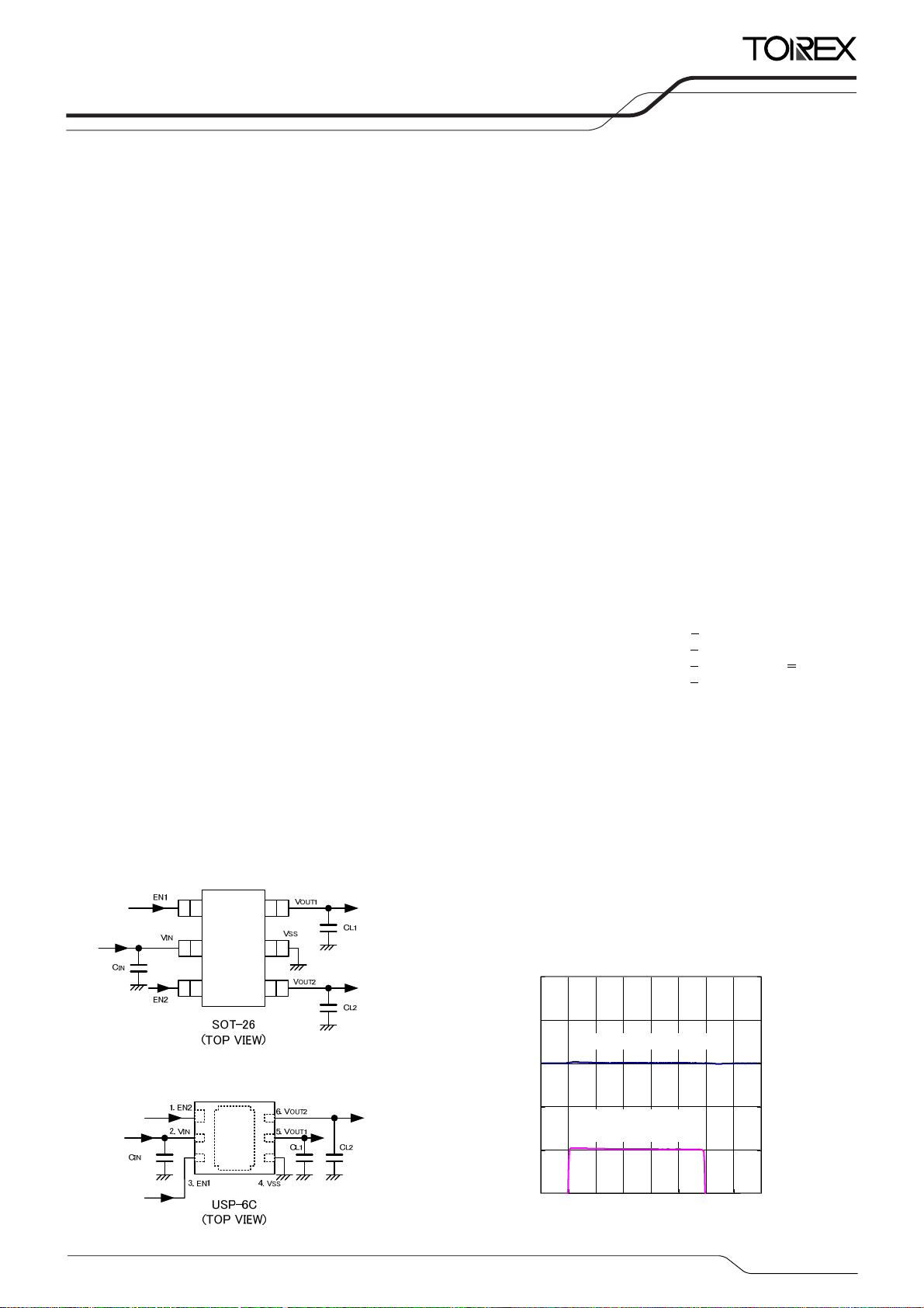
■TYPICAL APPLICATION CIRCUITS
) will be discharged via the internal auto-discharge switch, and as a result the V
L
) is also compatible with low ESR ceramic capacitors. The high level of output
L
■FEATURES
Output Current : 200mA (300mA limit, TYP.)
Dropout Voltage : 95mV @ I
V
Operating Voltage Range : 1.5V~6.0V
Output Voltage Range : 0.8V~5.0V
High Accuracy : + 1% @ V
+ 2% @ V
+ 20mV @V
+ 30mV @V
Low Power Consumption : 28μA/ch (TYP.)
Stand-by Current : Less than 0.1μA
Ripple Rejection : 65dB@1kHz
Operating Temperature Range : - 40OC ~ 85OC
Low ESR Capacitor : 1.0μF ceramic capacitors
Packages : USP-6C, SOT-26, USPN-6
Environmentally Friendly :
■TYPICAL PERFORMANCE
123
5
46
CHARACTERISTICS
● Cross Talk
(V)
Output Voltage(VR1) : V
OUT
3.40
3.35
3.30
3.25
3.20
3.15
XC6415(V
I
OUT2
OUT1
=0.1→50mA, CIN=CL1=CL2=1.0μF(ceramic)
Output Voltage(VR1 : 10mA)
Output Current
(VR2 : 0.1mA→50mA)
Time (200uS/div)
pin quickly returns to the VSS
OUT
OUT
OUT
(0.05V increments)
OUT
OUT
EU RoHS Compliant, Pb Free
=3.3V, V
V
=4.3V, tr=tf=5μS, Ta=25℃
IN
OUT2
=2.5V)
=100mA
=3.0V
>2.0V
≧1.5V
<2.0V
OUT
<1.5V
OUT
250
200
150
100
50
0
OUT
(mA)
Output Current(VR2) : I
1/24
XC6415 Series
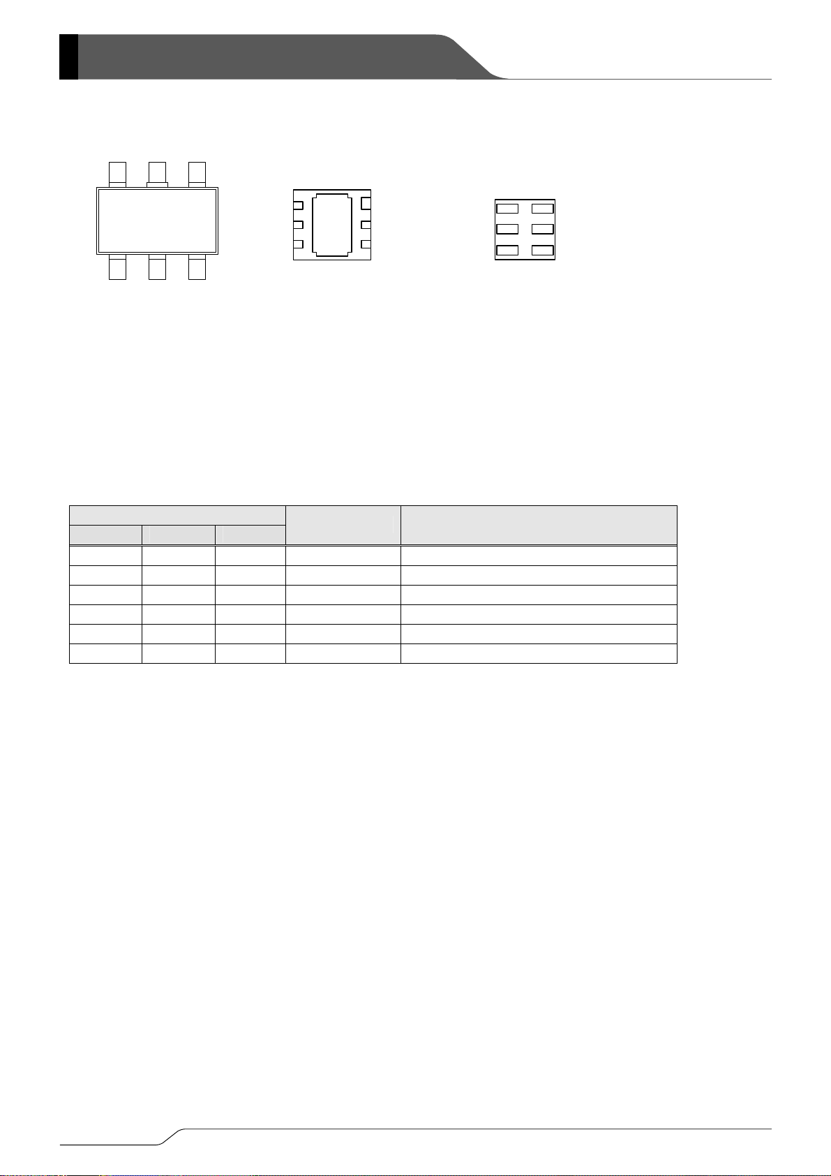
■PIN CONFIGURATION
OUT2VOUT1 VSS
■PIN ASSIGNMENT
6 4
1
EN1 VIN EN2
SOT-26
SOT-26
(TOP VIEW)
(TOP VIEW)
*The dissipation pad for the USP-6C package should be solder-plated in recommended mount
pattern and metal masking so as to enhance mounting strength and heat release. If the pad needs
to be connected to other pins, if should be connected to the V
PIN NUMBER
SOT-26 USP-6C USPN-6
1 3 3 EN1 ON/OFF Control 1
2 2 2
3 1 1 EN2 ON/OFF Control 2
4 6 6
5 4 4
6 5 5
2/24
V
5
V
OUT2 6
OUT1 5
V
SS 4
V
2
3
USP-6C *
USP-6C *
(BOTTOM VIEW)
(BOTTOM VIEW)
1 EN2
IN
2 V
3 EN1
(No. 4) pin.
SS
OUT2 6
V
OUT1 5
V
V
SS 4
USPN-6
USPN-6
(BOTTOM VIEW)
(BOTTOM VIEW)
PIN NAME FUNCTIONS
Power Input
Output 2
Ground
Output 1
V
VSS
V
VIN
OUT2
OUT1
1 EN2
IN
2 V
3 EN1
r
■PRODUCT CLASSIFICATION
●Ordering Information
XC6415①②③④⑤⑥-⑦
(*1)
DESIGNATOR DESCRIPTION SYMBOL DESCRIPTON
(without EN1 pulled down resistor) (Accuracy 1%) (without C
(without EN1 pulled down resistor) (Accuracy 1%) (with C
(without EN1 pulled down resistor) (Accuracy 2%) (without C
(without EN1 pulled down resistor) (Accuracy 2%) (with C
L
(with EN1 pulled down resistor) (Accuracy 1%) (without C
(with EN1 pulled down resistor) (Accuracy 1%) (with C
discharge)
L
(with EN1 pulled down resistor) (Accuracy 2%) (without C
(with EN1 pulled down resistor) (Accuracy 2%) (with C
discharge)
L
(without EN2 pulled down resistor) (Accuracy 1%) (without C
(without EN2 pulled down resistor) (Accuracy 1%) (with C
(without EN2 pulled down resistor) (Accuracy 2%) (without C
(without EN2 pulled down resistor) (Accuracy 2%) (with C
(with EN2 pulled down resistor) (Accuracy 1%) (without C
(with EN2 pulled down resistor) (Accuracy 1%) (with C
discharge)
L
(with EN2 pulled down resistor) (Accuracy 2%) (without C
(with EN2 pulled down resistor) (Accuracy 2%) (with CL discharge)
Refer to the table in the next page.
①
②
③④
Type of Regulator 1
(All EN High Active)
Type of Regulator 2
(All EN High Active)
Output Voltage -
A
B
C
D
E
F
G
H
A
B
C
D
E
F
G
H
MR-G SOT-26
MR SOT-26
ER-G USP-6C
ER USP-6C
⑤⑥-⑦
Packages
Taping Type
(*2)
7R-G USPN-6
(*1)
The “-G” suffix indicates that the products are Halogen and Antimony free as well as being fully RoHS compliant.
(*2)
The device orientation is fixed in its embossed tape pocket. For reverse orientation, please contact your local Torex sales office o
representative. (Standard orientation: ⑤R-⑦, Reverse orientation: ⑤L-⑦)
XC6415
Series
discharge)
L
discharge)
L
discharge)
L
discharge)
discharge)
L
discharge)
L
discharge)
L
discharge)
L
discharge)
L
discharge)
L
discharge)
L
discharge)
L
3/24
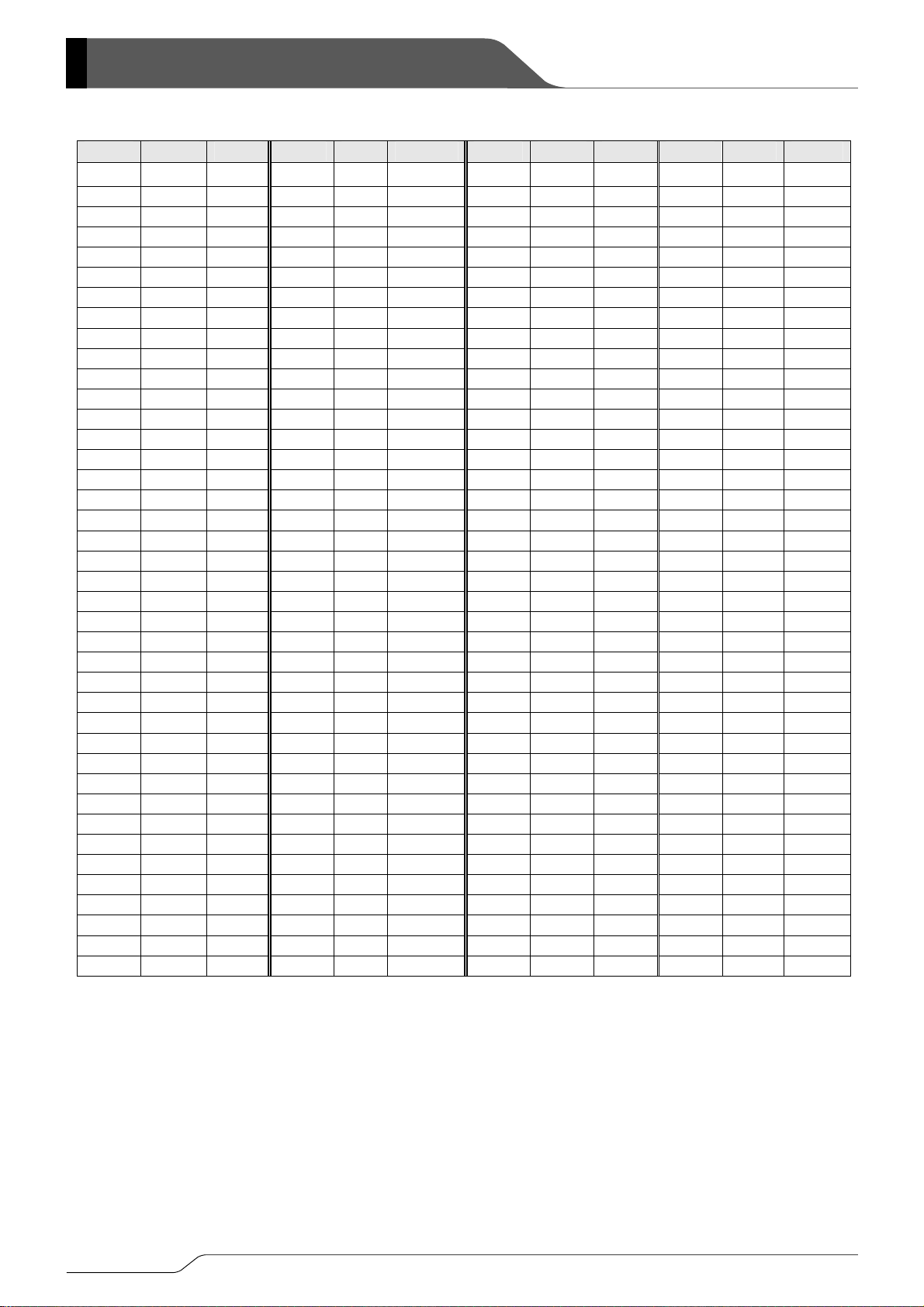
XC6415 Series
DESIGNATOR ③④
③④ VR1 VR2 ③④ VR1 VR2 ③④ VR1 VR2 ③④ VR1 VR2
01 1.80 2.80 41 2.80 3.00 81 2.00 3.30
02 1.20 2.90 42 2.90 1.80 82 3.30 2.00
03 1.80 1.80 43 3.00 1.80 83 2.80 1.20
04 1.50 2.70 44 2.50 1.80 84 1.00 3.30
05 2.85 2.85 45 1.80 2.85 85 2.70 2.70
06 1.80 3.30 46 1.50 1.20
07 3.00 3.00 47 2.85 1.50
08 2.80 1.80 48 3.20 3.20
09 1.20 1.20 49 1.20 3.00
10 1.10 1.30 50 2.60 2.85
11 1.30 1.50 51 4.20 3.10
12 2.80 2.80 52 5.00 3.60
13 2.50 3.30 53 1.80 1.20
14 3.00 3.30 54 2.60 3.00
15 1.20 1.80 55 2.60 2.60
16 2.80 3.30 56 1.80 2.60
17 3.30 3.30 57 2.60 3.30
18 3.10 3.10 58 2.50 2.90
19 2.80 1.50 59 1.80 2.70
20 1.30 2.80 60 1.00 2.80
21 1.50 2.80 61 3.00 1.50
22 1.80 3.00 62 2.70 1.80
23 1.85 2.80 63 2.80 2.70
24 1.85 3.30 64 2.80 3.10
25 2.60 2.80 65 2.85 3.30
26 1.50 1.50
27 2.00 3.00
28 3.30 1.80
29 3.30 1.75
30 2.10 4.10
31 1.20 2.80 71 3.00 2.95
32 1.50 1.80 72 3.00 3.05
33 1.50 3.00 73 3.10 2.90
34 1.50 3.30 74 3.10 2.95
35 1.50 2.60 75 3.10 3.00
36 2.00 2.50 76 3.10 3.05
37 3.30 4.50 77 3.00 3.10
38 2.50 2.50 78 1.20 2.60
39 1.80 2.50 79 3.50 3.50
40 1.20 2.50 80 1.10 1.50
*For other output voltage combinations, please contact your local Torex sales office or representative.
66 1.20 3.30
67 2.80 2.50
68 2.85 1.20
69 2.75 2.75
70 3.00 2.90
86
87
88
89
90
91
92
93
94
95
96
97
98
99
A0
A1
A2
A3
A4
A5
A6
A7
A8
A9
B0
B1
B2
B3
B4
B5
B6
B7
B8
B9
C0
2.70 3.30
2.90 2.90
2.50 2.80
2.50 3.00
4.50 4.50
3.30 5.00
3.00 5.00
1.80 2.90
1.10 1.80
1.20 1.30
1.00 1.20
1.50 2.50
1.20 0.90
3.15 3.15
3.10 1.80
1.80 2.00
1.50 1.30
2.85 2.60
1.25 2.50
1.85 1.20
3.30 1.20
1.80 1.95
2.85 3.00
1.55 2.80
1.90 1.90
2.50 2.85
3.00 1.00
1.30 1.80
2.70 3.00
2.80 1.90
2.50 0.90
3.15 2.85
2.60 1.30
3.00 2.50
3.30 1.10
C1
C2
C3
C4
C5
C6
C7
C8
C9
D0
D1
D2
D3
D4
D5
D6
D7
D8
D9
E0
E1
E2
3.30 2.50
1.85 2.85
1.50 2.90
1.80 3.20
1.00 2.50
3.10 2.80
3.00 3.60
1.30 3.00
1.50 2.40
3.30 3.60
1.00 2.85
1.80 1.85
3.60 1.50
3.00 2.80
4.50 2.60
2.00 1.80
3.30 3.10
3.20 3.10
3.40 3.10
3.10 2.50
2.50 3.10
3.40 3.40
4/24
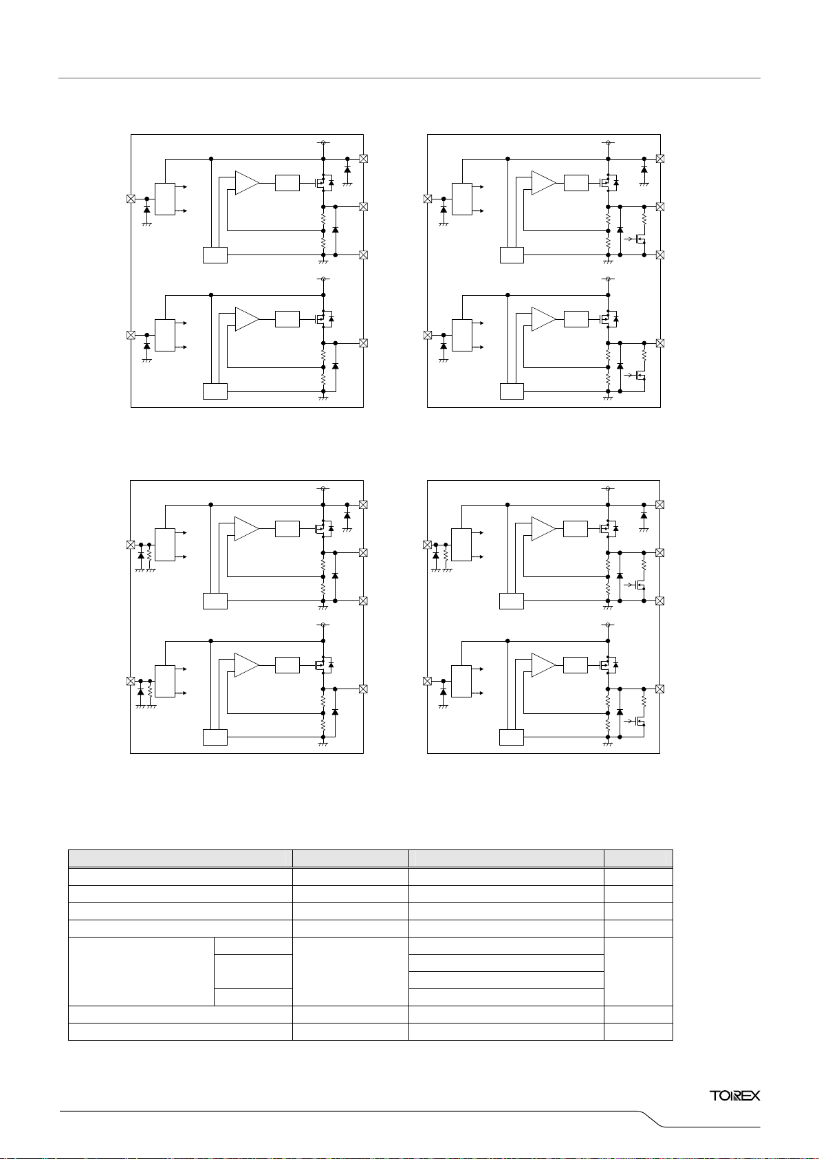
■BLOCK DIAGRAMS
V
IN
-
Error
Current
Amp1
EN1
VR1
each
EN1
EN2
ON/OFF
Control
ON/OFF
Control
circuit
EN1/
EN2
VR2
each
circuit
EN2/
Voltage
Reference
Voltage
Reference
+
-
+
Limit
EN1
R11
R12
Error
Current
Amp2
Limit
R21
R22
VOUT1
VSS
OUT2
V
EN2
ON/OFF
Control
ON/OFF
Control
EN1
VR1
each
circuit
EN1/
EN2
VR2
each
circuit
EN2/
Voltage
Reference
Voltage
Reference
-
Error
Current
Amp1
Limit
+
-
Error
Current
Amp2
Limit
+
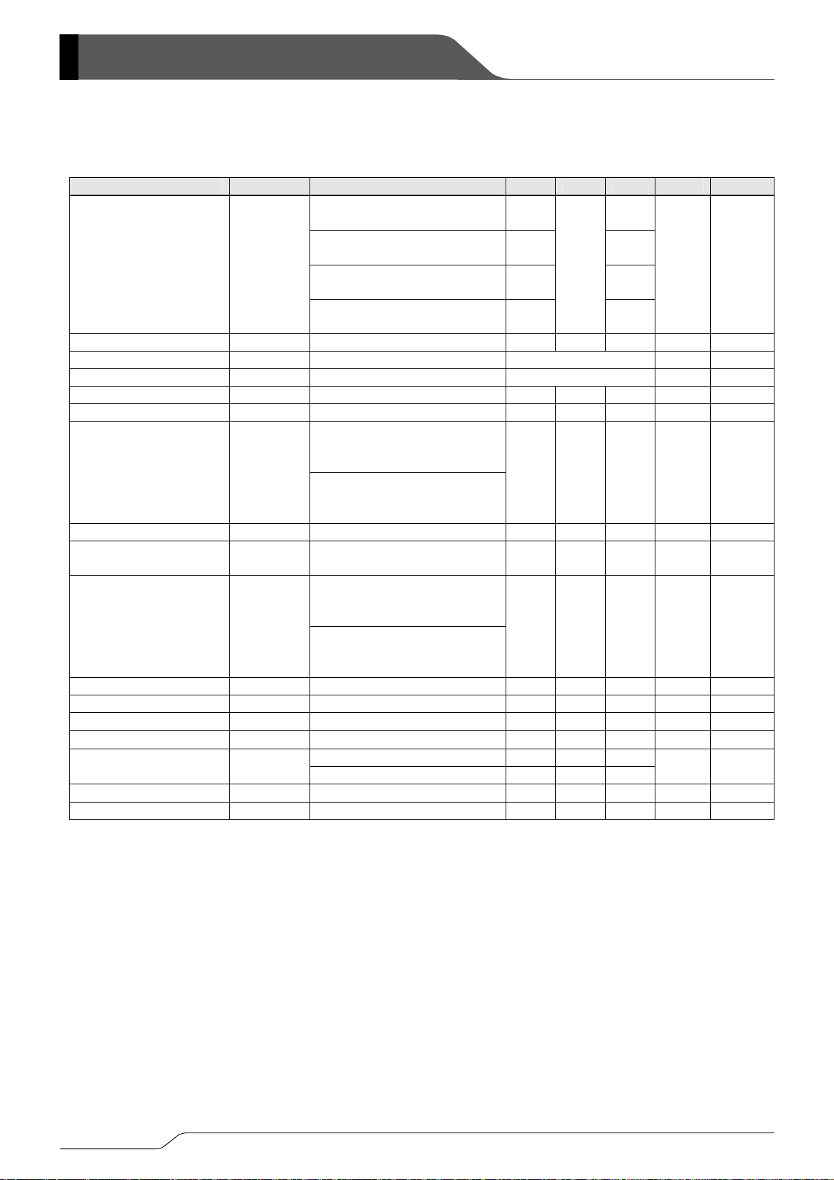
<XC6415AA, CC Series> <XC6415BB, DD Series>
IN
V
-
Error
Current
Amp1
EN1
VR1
each
EN1
ON/OFF
Control
circuit
EN1/
Voltage
Reference
+
Limit
EN1
R11
R12
VOUT1
VSS
ON/OFF
Control
EN1
VR1
each
circuit
EN1/
Voltage
Reference
-
Error
Current
Amp1
Limit
+
XC6415
Series
V
IN
Rdischg
Rdischg
Rdischg
VOUT1
VSS
V
V
VOUT1
VSS
OUT2
IN
R11
R12
EN1/
R21
R22
EN2/
R11
R12
EN1/
-
Error
Current
Amp2
EN2
VR2
EN2
ON/OFF
Control
circuit
EN2/
each
+
Voltage
Reference
Limit
EN2
OUT2
R21
R22
V
ON/OFF
Control
EN2
VR2
each
circuit
EN2/
<XC6415EE, GG Series> <XC6415FB, HD Series>
Voltage
Reference
-
Error
Amp2
+
* Diodes inside the circuits are ESD protection diodes and parasitic diodes.
■ABSOLUTE MAXIMUM RATINGS
PAR AMETER SYMBOL RATINGS UNITS
Input Voltage VIN - 0.3 ~ + 6.5 V
Output Current I
Output Voltage 1 / Output Voltage 2 V
EN1/EN2 Input Voltage V
OUT1
OUT1
EN1
+ I
500
OUT2
/ V
V
OUT2
/ V
V
EN2
SS
SS
SOT-26 250
Power Dissipation
USP-6C
Pd
1000 (PCB mounted)
USPN-6
Operating Temperature Range Topr - 40 ~ + 85 ℃
Storage Temperature Range Ts tg - 55 ~ + 125 ℃
*1: Please use within the range of Pd > { (VIN-V
OUT1
)×I
OUT1
+ (VIN-V
OUT2
)×I
OUT2
*2: The power dissipation figure shown is PCB mounted. Please refer to page 21 for details.
(*1)
mA
- 0.3 ~ V
+ 0.3 V
IN
- 0.3 ~ + 6.5 V
100
100
}
Current
Limit
OUT2
R21
R22
EN2/
V
Rdischg
Ta =2 5OC
(*2)
mW
5/24
T
XC6415 Series
■ELECTRICAL CHARACTERISTICS
● XC6415 Series
Regulator 1, Regulator 2
PAR AMETER SYMBOL CONDITIONS MIN. TYP. MAX. UNITS CIRCUITS
V
≧2.0V,
OUT(T)
V
Output Voltage
Output Current I
Load Regulation ΔV
Dropout Voltage
(*5)
Vdif I
Supply Current ISS V
Stand-by Current I
Line Regulation
OUT(E)
(*2)
OUTMAX
OUT
STBY
ΔV
OUT/
(ΔVIN・V
200 - - mA ①
VEN=V
IN=VEN=VOUT(T)
V
)
OUT
V
OUT(T)
V
V
V
V
OUT
V
V
, I
EN=VIN
V
OUT
EN=VIN
V
OUT(T)
EN=VIN、IOUT
V
OUT
EN=VIN、IOUT
0.1mA≦I
IN,
=10mA
OUT
≦1.95V,
, I
=10mA
OUT
≧1.5V
=10mA
≦1.45V
=10mA
OUT
≦100mA E-1 mV ①
=100mA, VEN=VIN E-2 mV ①
+1.0V, I
=6.0V, VEN=VSS - 0.01 0.10 μA ②
IN
=0mA - 28 60 μA ②
OUT
+0.5V≦VIN≦6.0V
:V
EN=VIN
1.5V≦V
:V
EN=VIN
OUT(T)
OUT(T)
≧1.0V,
, I
OUT
≦6.0V
IN
≦0.95V
, I
OUT
=10mA
=10mA
Input Voltage VIN 1.5 - 6.0 V ①
Output Voltage
emperature Characteristics
(ΔTa ・V
Ripple Rejection Rate PSRR
Limit Current I
Short Current I
EN ”H” Level Voltage V
EN ”L” Level Voltage V
EN ”H” Level Current I
EN ”L” Level Current I
OUT1
(*6)
(*8)
}
R
IN=VOUT(T)
OUT(E)
OUT1
CL Discharge Resistor
NOTE:
*1) Unless otherwise stated, V
*2) V
(ie. The output voltage when “V
*3) Characteristics of the actual V
*4) V
*5) Vdif={V
*6) V
*7) V
*8) For XC6415B, D, F, H series only.
*9) Each channel is measured when the other channel is turned off (V
= Effective output voltage (see the voltage chart)
OUT(E)
: Nominal output voltage
OUT(T)
(*7)
- V
IN1
: A voltage equal to 98% of the output voltage whenever an amply stabilized I
OUT1
: The input voltage when V
IN1
XC6415A, C, E, G series discharge with only Rx1 and Rx2 resistors as shown in the BLOCK DIAGRAMS.
/
ΔV
OUT
)
OUT
V
LIM
VEN=VIN, Short V
SHORT
ENH
ENL
ENH
V
ENL
VIN=6.0V, V
DCHG
V
VIN={V
OUT(T)
V
EN=VIN
V
IN
V
EN=VIN
VEN=VIN(A~D Series) -0.1 - 0.1
V
EN=VIN
, I
EN=VIN
OUT
=30mA
-40℃≦Ta ≦85℃
+1.0}VDC+0.5Vp-pAC
: V
≦4.75V,
OUT(T)
, I
=30mA, f=1kHz
OUT
=5.75VDC+0.5Vp-pAC
: V
≧4.8V,
OUT(T)
, I
=30mA, f=1kHz
OUT
EN=VIN
OUT
210 300 - mA ①
to VSS level - 20 - mA ①
=6V(E~H Series) - 3.0 -
EN=VSS
=4.0V, VCE=VSS - 550 - Ω ①
OUT
+1.0V.
+1.0V” is provided at the VIN pin while maintaining a certain I
OUT(T)
by setting output voltage is shown in the voltage chart.
appears as input voltage is gradually decreased.
).
EN=VSS
×0.99
(*3)
-0.02
(*3)
×0.98
(*3)
-0.03
(*3)
- 0.01 0.20 %/V ①
- ±100 - ppm/℃
- 65 - dB ③
1.2 - 6.0
- - 0.3
-0.1 - 0.1
OUT{VOUT(T)
+1.0V} is input.
V
OUT
OUT(T)
(*4)
value.
×1.01
(*3)
+0.02
(*3)
×1.02
(*3)
+0.03
(*3)
Ta =2 5 ℃
V ①
V
V
μA
μA
①
①
①
①
①
6/24
■ELECTRICAL CHARACTERISTICS (Continued)
●Voltage Chart
NOMINAL
OUTPUT
VOLTAGE
(V)
V
OUT(T)
OUTPUT VOLTAGE
(V)
V
1% Accuracy
OUT(E)
V
2% Accuracy △V
OUT(E)
MIN. MAX. MIN. MAX. TYP. MAX. TYP. MAX.
LOAD REGULATION
E-1
(mV)
OUT
0.80 0.7800 0.8200 0.7700 0.8300
0.85 0.8300 0.8700 0.8200 0.8800
0.90 0.8800 0.9200 0.8700 0.9300
0.95 0.9300 0.9700 0.9200 0.9800
1.00 0.9800 1.0200 0.9700 1.0300
1.05 1.0300 1.0700 1.0200 1.0800
1.10 1.0800 1.1200 1.0700 1.1300
1.15 1.1300 1.1700 1.1200 1.1800
1.20 1.1800 1.2200 1.1700 1.2300
1.25 1.2300 1.2700 1.2200 1.2800
1.30 1.2800 1.3200 1.2700 1.3300
1.35 1.3300 1.3700 1.3200 1.3800
1.40 1.3800 1.4200 1.3700 1.4300
10 30
1.45 1.4300 1.4700 1.4200 1.4800
1.50 1.4800 1.5200 1.4700 1.5300
1.55 1.5300 1.5700 1.5190 1.5810
1.60 1.5800 1.6200 1.5680 1.6320
1.65 1.6300 1.6700 1.6170 1.6830
1.70 1.6800 1.7200 1.6660 1.7340
1.75 1.7300 1.7700 1.7150 1.7850
1.80 1.7800 1.8200 1.7640 1.8360
1.85 1.8300 1.8700 1.8130 1.8870
1.90 1.8800 1.9200 1.8620 1.9380
1.95 1.9300 1.9700 1.9110 1.9890
2.00 1.9800 2.0200 1.9600 2.0400
2.05 2.0295 2.0705 2.0090 2.0910
2.10 2.0790 2.1210 2.0580 2.1420
2.15 2.1285 2.1715 2.1070 2.1930
2.20 2.1780 2.2220 2.1560 2.2440
2.25 2.2275 2.2725 2.2050 2.2950
2.30 2.2770 2.3230 2.2540 2.3460
2.35 2.3265 2.3735 2.3030 2.3970
2.40 2.3760 2.4240 2.3520 2.4480
2.45 2.4255 2.4745 2.4010 2.4990
2.50 2.4750 2.5250 2.4500 2.5500
20 50
2.55 2.5245 2.5755 2.4990 2.6010
2.60 2.5740 2.6260 2.4580 2.6520
2.65 2.6235 2.6765 2.8970 2.7030
2.70 2.6730 2.7270 2.6460 2.7540
2.75 2.7225 2.7775 2.6950 2.8050
2.80 2.7720 2.8280 2.7440 2.8560
2.85 2.8215 2.8785 2.7930 2.9070
2.90 2.8710 2.9290 2.8420 2.9580
2.95 2.9205 2.9795 2.8910 3.0090
XC6415
Series
DROPOUT VOLTAGE
E-2
(mV)
500
410
Vdif
850
750
360 600
330 600
280
240
200
180
170
420
360
300
260
240
150 200
120
180
110
95
150
7/24
XC6415 Series
■ELECTRICAL CHARACTERISTICS (Continued)
●Voltage Chart (Continued)
NOMINAL
OUTPUT
VOLTAGE
(V)
V
OUT(T)
V
OUT(E)
MIN. MAX. MIN. MAX. TYP. MAX. TYP. MAX.
OUTPUT VOLTAGE
1% Accuracy
(V)
V
2% Accuracy △V
OUT(E)
3.00 2.9700 3.0300 2.9400 3.0600
3.05 3.0195 3.0805 2.9890 3.1110
3.10 3.0690 3.1310 3.0380 3.1620
3.15 3.1185 3.1815 3.0870 3.2130
3.20 3.1680 3.2320 3.1360 3.2640
3.25 3.2175 3.2825 3.1850 3.3150
3.30 3.2670 3.3330 3.2340 3.3660
3.35 3.3165 3.3835 3.2830 3.4170
3.40 3.3660 3.4340 3.3320 3.4680
3.45 3.4155 3.4845 3.3810 3.5190
3.50 3.4650 3.5350 3.4300 3.5700
3.55 3.5145 3.5855 3.4790 3.6210
3.60 3.5640 3.6360 3.5280 3.6720
3.65 3.6135 3.6865 3.5770 3.7230
3.70 3.6630 3.7370 3.6260 3.7740
3.75 3.7125 3.7875 3.6750 3.8250
3.80 3.7620 3.8380 3.7240 3.8760
3.85 3.8115 3.8885 3.7730 3.9270
3.90 3.8610 3.9390 3.8220 3.9780
3.95 3.9105 3.9895 3.8710 4.0290
4.00 3.9600 4.0400 3.9200 4.0800
4.05 4.0095 4.0905 3.9690 4.1310
4.10 4.0590 4.1410 4.0180 4.1820
4.15 4.1085 4.1915 4.0670 4.2330
4.20 4.1580 4.2420 4.1160 4.2840
4.25 4.2075 4.2925 4.1650 4.3350
4.30 4.2570 4.3430 4.2140 4.3860
4.35 4.3065 4.3935 4.2630 4.4370
4.40 4.3560 4.4440 4.3120 4.4880
4.45 4.4055 4.4945 4.3610 4.5390
4.50 4.4550 4.5450 4.4100 4.5900
4.55 4.5045 4.5955 4.4590 4.6410
4.60 4.5540 4.6460 4.5080 4.6920
4.65 4.6035 4.6965 4.5570 4.7430
4.70 4.6530 4.7470 4.6060 4.7940
4.75 4.7025 4.7975 4.6550 4.8450
4.80 4.7520 4.8480 4.7040 4.8960
4.85 4.8015 4.8985 4.7530 4.9470
4.90 4.8510 4.9490 4.8020 4.9980
4.95 4.9005 4.9995 4.8510 5.0490
5.00 4.9500 5.0500 4.9000 5.1000
LOAD REGULATION
E-1
(mV)
OUT
20 50 150
30 60
DROPOUT VOLTAGE
E-2
(mV)
Vdif
95
80
120
8/24

XC6415
■OPERATIONAL DESCRIPTION
<Output Voltage Control>
The voltage divided by resistors Rx1 and Rx2 is compared with the internal reference voltage by the error amplifier. The
P-channel MOSFET which is connected to the V
the V
OUT pin is controlled and stabilized by a system of negative feedback. The current limit circuit and short protect circuit
operate in relation to the level of output current. Further, the IC's internal circuitry can be shutdown via the EN pin's signal.
<CL Auto-Discharge Function>
XC6415B, D, F, H series can quickly discharge the electric charge at the output capacitor (C
pin, which enables a whole IC circuit put into OFF state, is inputted via the N-channel transistor located between the VOUT
pin and the V
is 4.0V (TYP.). Moreover, discharge time of the output capacitor (CL) is set by the CL auto-discharge resistance (R) and the
output capacitor (CL). By setting time constant of a CL auto-discharge resistance value [R] and an output capacitor value
L) as τ(τ=C x R), the output voltage after discharge via the N channel transistor is calculated by the following formulas.
(C
( V : Output voltage after discharge, V
C
<Current Limiter, Short-Circuit Protection>
<EN Pin>
■NOTES ON USE
L auto-discharge resistance R×Output capacitor (CL) value C)
τ: C
high-speed discharge function can be set by each regulator.
L
The XC6415 series includes a fold-back circuit, which aid the operations of the current limiter and circuit protection. When
the load current reaches the current limit level, the fold-back circuit operates and output voltage drops. As a result of this
drop in output voltage, output current also decreases. When the output pin is shorted, a current of about 20mA flows.
The IC's internal circuitry can be shutdown via the signal from the EN pin with the XC6415 series. In shutdown mode,
output at the V
the CL auto-discharge resistor is connected in parallel to Rx1 and Rx2 while the power supply is applied to the VIN pin.
Therefore, time until the VOUT pin reaches the VSS level becomes short. The EN pin is CMOS input, but in case the EN
pin with pulled down resistor, the EN input current will be increase when the IC operates. Also, in case of the EN pin
without pulled down resistor, the output voltage becomes unstable when the EN pin is left open. If this IC is used with the
correct output voltage for the EN pin, the logic is fixed and the IC will operate normally. However, supply current may
increase as a result of through current in the IC's internal circuitry when medium voltage is input.
. Please use this IC within the stated absolute maximum ratings. The IC is liable to malfunction should the ratings be
1
exceeded.
2. Where wiring impedance is high, operations may become unstable due to noise and/or phase lag depending on output
current. Please wire the input capacitor (CIN) and the output capacitor (CL) as close to the IC as possible.
SS pin (cf. BLOCK DIAGRAM). The C
OUT(E) : Output voltage, t: Discharge time,
OUT pin will be pulled down to the VSS level via Rx1 & Rx2. However, as for the XC6415B, D, F, H series,
OUT pin is then driven by the subsequent output signal. The output voltage at
< XC6415BB Series >
L), when a low signal to the EN
discharge resistance is set to 550Ω when VIN is 6.0V (TYP.) and V
L
–t/
V = VOUT x e
τ
, or t=τln( VOUT
/ V )
(E)
Series
OUT
9/24

XC6415 Series
■TEST CIRCUITS
●Circuit ①
●Circuit ②
●Circuit ③
10/24

■TYPICAL PERFORMANCE CHARACTERISTICS
* EN Voltage condition: Unless otherwise stated, VEN=V
(1) OutputVoltage vs. OutputCurrent
IN
XC6415
Series
XC6415(V
V
=1.8V, CIN=1.0μF(ceramic), CL=1.0μF(ceramic)
IN
OUT
=0.8V)
1
0.8
(V)
OUT
0.6
0.4
0.2
OutputVoltage : V
0
0 50 100 150 200 250 300 350 400
OUT
OUT
=1.5V)
(mA)
OutputCurrent : I
XC6415(V
V
=2.5V, CIN=1.0μF(ceramic), CL=1.0μF(ceramic)
IN
1.8
1.5
(V)
OUT
1.2
Ta=85℃
Ta=25℃
Ta=-40℃
XC6415(V
V
=1.8V, CIN=1.0μF(ceramic), CL=1.0μF(ceramic)
IN
OUT
=0.8V)
1
0.8
(V)
OUT
0.6
0.4
0.2
OutputVoltage : V
0
0 50 100 150 200 250 300 350 400
OutputCurrent : I
XC6415(V
V
=2.5V, CIN=1.0μF(ceramic), CL=1.0μF(ceramic)
IN
OUT
OUT
=1.5V)
1.8
1.5
(V)
OUT
1.2
VIN=1.6V
VIN=1.8V
VIN=2.3V
VIN=6.0V
(mA)
0.9
0.6
OutputVoltage : V
0.3
0
0 50 100 150 200 250 300 350 400
OUT
OUT
=2.8V)
(mA)
3.2
OutputCurrent : I
XC6415(V
V
=3.8V, CIN=1.0μF(ceramic), CL=1.0μF(ceramic)
IN
2.8
(V)
2.4
OUT
2.0
1.6
1.2
0.8
OutputVoltage : V
0.4
0.0
0 50 100 150 200 250 300 350 400
OutputCurrent : I
OUT
(mA)
Ta=85℃
Ta=25℃
Ta=-40℃
Ta=85℃
Ta=25℃
Ta=-40℃
0.9
0.6
OutputVoltage : V
0.3
0
0 50 100 150 200 250 300 350 400
OUT
OUT
=2.8V)
(mA)
OutputCurrent : I
XC6415(V
V
=3.8V, CIN=1.0μF(ceramic), CL=1.0μF(ceramic)
IN
3.2
2.8
(V)
2.4
OUT
2.0
1.6
1.2
0.8
OutputVoltage : V
0.4
0.0
0 50 100 150 200 250 300 350 400
OutputCurrent : I
OUT
(mA)
VIN=1.6V
VIN=1.8V
VIN=2.0V
VIN=2.5V
VIN=6.0V
VIN=2.9V
VIN=3.1V
VIN=3.3V
VIN=3.8V
VIN=6.0V
11/24

XC6415 Series
■TYPICAL PERFORMANCE CHARACTERISTICS (Continued)
(1) OutputVoltage vs. OutputCurrent
XC6415(V
V
=6.0V, CIN=1.0μF(ceramic), CL=1.0μF(ceramic)
6
IN
5
(V)
OUT
4
3
2
OutputVoltage : V
1
0
0 50 100 150 200 250 300 350 400
OutputCurrent : I
OUT
=5.0V)
(2) OutputVoltage vs. InputVoltage
XC6415(V
C
IN
1.0
0.9
0.8
(V)
0.7
OUT
0.6
0.5
0.4
0.3
0.2
OutputVoltage : V
0.1
0.0
0.0 1.0 2.0 3.0 4.0 5.0 6.0
InputVoltage : V
=0.8V)
OUT
=1.0μF(ceramic), CL=1.0μF(ceramic)
(Continued)
(mA)
OUT
IOUT=1mA
IOUT=10mA
IOUT=30mA
IOUT=100mA
(V)
IN
Ta=85℃
Ta=25℃
Ta=-40℃
Ta=25℃
XC6415(V
V
=6.0V, CIN=1.0μF(ceramic), CL=1.0μF(ceramic)
6
IN
OUT
=5.0V)
5
(V)
OUT
4
3
2
OutputVoltage : V
1
VIN=5.1V
VIN=5.3V
VIN=5.5V
VIN=6.0V
0
0 50 100 150 200 250 300 350 400
OutputCurrent : I
XC6415(V
C
=1.0μF(ceramic), CL=1.0μF(ceramic)
IN
OUT
(mA)
OUT
=0.8V)
0.90
0.85
(V)
OUT
0.80
0.75
IOUT=1mA
0.70
OutputVoltage : V
IOUT=10mA
IOUT=30mA
IOUT=100mA
0.65
1.5 2.0 2.5 3.0 3.5 4.0 4.5 5.0 5.5 6.0
InputVoltage : V
IN
(V)
Ta=25℃
(V)
OUT
OutputVoltage : V
12/24
XC6415(V
C
IN
=1.5V)
OUT
=1.0μF(ceramic), CL=1.0μF(ceramic)
2.0
1.5
1.0
0.5
0.0
IOUT=1mA
IOUT=10mA
IOUT=30mA
IOUT=100mA
0.0 1.0 2.0 3.0 4.0 5.0 6.0
InputVoltage : V
(V)
IN
Ta=25℃
XC6415(V
C
1.60
1.55
(V)
OUT
IN
=1.5V)
OUT
=1.0μF(ceramic), CL=1.0μF(ceramic)
1.50
1.45
1.40
OutputVoltage : V
1.35
2.5 3.0 3.5 4.0 4.5 5.0 5.5 6.0
InputVoltage : V
IN
(V)
Ta=25℃
IOUT=1mA
IOUT=10mA
IOUT=30mA
IOUT=100mA

■TYPICAL PERFORMANCE CHARACTERISTICS (Continued)
XC6415
Series
(2) OutputVoltage vs. InputVoltage
XC6415(V
3.2
2.8
(V)
2.4
OUT
2.0
1.6
1.2
0.8
OutputVoltage : V
0.4
0.0
0.0 1.0 2.0 3.0 4.0 5.0 6.0
InputVoltage : V
XC6415(V
6.0
OUT
C
=1.0μF(ceramic), CL=1.0μF(ceramic)
IN
OUT
C
=1.0μF(ceramic), CL=1.0μF(ceramic)
IN
(Continued)
=2.8V)
(V)
IN
=5.0V)
Ta=25℃
IOUT=1mA
IOUT=10mA
IOUT=30mA
IOUT=100mA
Ta=25℃
(V)
OUT
2.90
2.85
XC6415(V
C
=2.8V)
OUT
=1.0μF(ceramic), CL=1.0μF(ceramic)
IN
2.80
2.75
2.70
OutputVoltage : V
2.65
3.5 4.0 4.5 5.0 5.5 6.0
OUT
IN
=5.0V)
(V)
5.10
InputVoltage : V
XC6415(V
C
=1.0μF(ceramic), CL=1.0μF(ceramic)
IN
Ta=25℃
IOUT=1mA
IOUT=10mA
IOUT=30mA
IOUT=100mA
Ta=25℃
5.0
(V)
OUT
4.0
3.0
2.0
1.0
OutputVoltage : V
0.0
0.0 1.0 2.0 3.0 4.0 5.0 6.0
InputVoltage : V
(3) DropoutVoltage vs. OutputCurrent
XC6415(V
C
1.0
IN
0.9
0.8
※ Below the minimum operating
0.7
0.6
0.5
0.4
0.3
0.2
DropoutVoltage : Vdif (V)
0.1
0.0
0 50 100 150 200
OutputCurrent : I
=0.8V)
OUT
=1.0μF(ceramic), CL=1.0μF(ceramic)
OUT
(V)
IN
(mA)
IOUT=1mA
IOUT=10mA
IOUT=30mA
IOUT=100mA
Ta=85℃
Ta=25℃
Ta=-40℃
5.05
(V)
OUT
5.00
4.95
4.90
OutputVoltage : V
4.85
5.2 5.4 5.6 5.8 6
OUT
IN
=1.5V)
(V)
InputVoltage : V
XC6415(V
C
=1.0μF(ceramic), CL=1.0μF(ceramic)
IN
0.5
0.4
0.3
0.2
Dropout Voltage: Vdif (V)
0.1
OutputVoltage : Vdif (V)
0.0
0 50 100 150 200
OutputCurrent : I
OUT
(mA)
IOUT=1mA
IOUT=10mA
IOUT=30mA
IOUT=100mA
Ta=85℃
Ta=25℃
Ta=-40℃
13/24

XC6415 Series
■TYPICAL PERFORMANCE CHARACTERISTICS (Continued)
(3) DropoutVoltage vs. OutputCurrent
XC6415(V
C
0.5
IN
0.4
0.3
0.2
0.1
DropoutVoltage : Vdif (V)
0.0
0 50 100 150 200
OutputCurrent : I
=2.8V)
OUT
=1.0μF(ceramic), CL=1.0μF(ceramic)
OUT
(4) SupplyCurrent vs. InputVoltage
XC6415(V
60
50
(μA)
40
SS
OUT
=0.8V)
(Continued)
Ta=85℃
Ta=25℃
Ta=-40℃
(mA)
Ta=85℃
Ta=25℃
Ta=-40℃
0.5
XC6415(V
C
IN
=5.0V)
OUT
=1.0μF(ceramic), CL=1.0μF(ceramic)
0.4
0.3
0.2
Dropout Voltage: Vdif (V)
0.1
OutputVoltage : Vdif (V)
0.0
0 50 100 150 200
OUT
OUT
=1.5V)
(mA)
OutputCurrent : I
XC6415(V
60
50
(μA)
40
SS
Ta=85℃
Ta=25℃
Ta=-40℃
Ta=85℃
Ta=25℃
Ta=-40℃
30
20
SupplyCurrent : I
10
0
0123456
OUT
IN
=2.8V)
(V)
InputVoltage : V
XC6415(V
60
Ta=85℃
50
(μA)
40
SS
Ta=25℃
Ta=-40℃
30
20
SupplyCurrent : I
10
30
20
SupplyCurrent : I
10
0
0123456
OUT
IN
=5.0V)
(V)
InputVoltage : V
XC6415(V
60
Ta=85℃
50
(μA)
40
SS
Ta=25℃
Ta=-40℃
30
20
SupplyCurrent : I
10
14/24
0
0123456
InputVoltage : V
(V)
IN
0
0123456
InputVoltage : V
IN
(V)

■TYPICAL PERFORMANCE CHARACTERISTICS (Continued)
(5) OutputVoltage vs. AmbientTemperature
XC6415
Series
XC6415(V
V
=1.8V, CIN=1.0μF(ceramic), CL=1.0μF(ceramic)
IN
OUT
=0.8V)
0.90
(V)
0.85
OUT
0.80
0.75
OutputVoltage : V
0.70
-50 -25 0 25 50 75 100
AmbientTemperature : Ta (℃)
(V)
OUT
2.90
2.85
XC6415(V
VIN=3.8V, C
IN
=2.8V)
OUT
=1.0μF(ceramic), CL=1.0μF(ceramic)
IOUT=1mA
IOUT=10mA
IOUT=30mA
IOUT=100mA
2.80
IOUT=1mA
IOUT=10mA
IOUT=30mA
IOUT=100mA
(V)
OUT
1.60
1.55
XC6415(V
V
=2.5V, CIN=1.0μF(ceramic), CL=1.0μF(ceramic)
IN
OUT
=1.5V)
1.50
IOUT=1mA
IOUT=10mA
IOUT=30mA
IOUT=100mA
OutputVoltage : V
1.45
1.40
-50 -25 0 25 50 75 100
AmbientTemperature : Ta (℃)
XC6415(V
5.20
(V)
5.10
OUT
VIN=6.0V, C
IN
=5.0V)
OUT
=1.0μF(ceramic), CL=1.0μF(ceramic)
5.00
IOUT=1mA
IOUT=10mA
IOUT=30mA
IOUT=100mA
2.75
OutputVoltage : V
2.70
-50 -25 0 25 50 75 100
AmbientTemperature : Ta (℃)
4.90
OutputVoltage : V
4.80
-50 -25 0 25 50 75 100
AmbientTemperature : Ta (℃)
(6) SupplyCurrent vs. AmbientTemperature (7) EN Threshold Voltage vs. AmbientTemperature
XC6415
V
50
IN=VOUT
40
(μA)
SS
30
20
10
SupplyCurrent : I
VOUT=0.8V
VOUT=1.5V
VOUT=2.8V
VOUT=5.0V
0
-50 -25 0 25 50 75 100
AmbientTemperature : Ta (℃)
+1.0V
1.2
1.0
(V)
EN
(μA)
0.8
SS
0.6
0.4
SupplyCurrent : I
0.2
EN Threshold Voltage : V
0.0
-50 -25 0 25 50 75 100
AmbientTemperature : Ta (℃)
XC6415
EN"H"LEVEL
EN"L"LEVEL
15/24

XC6415 Series
■TYPICAL PERFORMANCE CHARACTERISTICS (Continued)
(8) Rising Response Time
(V)
Input Voltage : V
(V)
IN
IN
3.0
2.0
1.0
0.0
-1.0
-2.0
-3.0
6.0
4.0
2.0
0.0
XC6415(V
Time (40μs/div) Time (40μs/div)
Time (40uS/div)
XC6415(V
=0.8V)
OUT
V
=0→1.8V, CL=1.0μF(ceramic)
IN
Input Vo ltage
Output Voltage
V
=0→3.8V, CL=1.0μF(ceramic)
IN
Input Vo ltage
tr=5μS, Ta=25℃
=2.8V)
OUT
tr=5μS, Ta=25℃
Output Voltage
I
OUT
=0.1mA
1mA
30mA
100mA
3.0
2.5
2.0
1.5
1.0
0.5
0.0
6.0
5.0
4.0
3.0
XC6415(V
3.0
2.0
(V)
OUT
(V)
IN
1.0
OUT
V
=0→2.5V, CL=1.0μF(ceramic)
IN
Input Voltage
Output Voltage
0.0
-1.0
Output Voltage : V
Input Voltage : V
-2.0
-3.0
Time (40uS/div)
XC6415(V
8.0
OUT
V
=0→6.0V, CL=1.0μF(ceramic)
IN
Input Voltage
6.0
(V)
OUT
(V)
IN
4.0
2.0
=1.5V)
tr=5μS, Ta=25℃
I
OUT
=5.0V)
tr=5μS, Ta=25℃
Output
=0.1mA
1mA
30mA
100mA
3.0
2.5
2.0
1.5
1.0
0.5
0.0
12.0
10.0
8.0
6.0
(V)
OUT
Output Voltage : V
(V)
OUT
-2.0
Input Voltage : V
-4.0
-6.0
Time (40μs/div) Time (40μs/div)
Time (40uS/div)
(9) Input Transient Response
XC6415(VOUT=0.8V)
3.8
2.8
1.8
0.8
-0.2
Input Voltage : VIN (V)
-1.2
-2.2
VIN=1.8⇔2.8V, CL=1.0μF(ceramic)
Input Voltage
Output Voltage
Time (100uS/div)
I
=0.1mA
OUT
1mA
30mA
100mA
tr=tf=5μS, Ta=25℃
IOUT=0.1mA
IOUT=1mA
IOUT=30mA
IOUT=100mA
2.0
1.0
0.0
1.00
0.95
0.90
0.85
0.80
0.75
0.70
1mA
4.0
2.0
0.0
Output Voltage : V
0.0
I
=0.1mA
Output Voltage : V
Input Voltage : V
-2.0
OUT
30mA
100mA
-4.0
Time (40uS/div)
XC6415(VOUT=1.5V)
4.5
VIN=2.5⇔3.5V, CL=1.0μF(ceramic)
Input Voltage
3.5
2.5
1.5
Output Voltage
0.5
Output Voltage : VOUT (V)
Input Voltage : VIN (V)
-0.5
-1.5
Time (100μs/div) Time (100μs/div)
Time (100uS/div)
tr=tf=5μS, Ta=25℃
IOUT=0.1mA
IOUT=1mA
IOUT=30mA
IOUT=100mA
1.70
1.65
1.60
1.55
1.50
1.45
1.40
Output Voltage : VOUT (V)
16/24

t
■TYPICAL PERFORMANCE CHARACTERISTICS (Continued)
XC6415
Series
(9) Input Transient Response
XC6415(VOUT=2.8V)
5.8
VIN=3.8⇔4.8V, CL=1.0μF(ceramic)
Input Voltage
4.8
3.8
2.8
Output Voltage
1.8
Input Voltage : VIN (V)
0.8
-0.2
Time (100μs/div) Time (100μs/div)
Time (100uS/div)
(10) Load Transient Response
XC6415(V
V
=1.8V, tr=tf=5μS, Ta=25℃
IN
=0.1→50mA, CIN=CL=1.0μF(ceramic)
I
OUT
Output Voltage
(V)
0.85
0.80
OUT
0.75
(Continued)
tr=tf=5μS, Ta=25℃
IOUT=0.1mA
IOUT=1mA
IOUT=30mA
IOUT=100mA
=0.8V)
OUT
3.00
2.95
2.90
2.85
2.80
2.75
2.70
250
200
150
XC6415(VOUT=5.0V)
6.5
VIN=5.5⇔6.0V, CL=1.0μF(ceramic)
Input Voltage
6.0
5.5
5.0
Output Voltage
4.5
Output Voltage : VOUT (V)
Input Voltage : VIN (V)
4.0
3.5
r=tf=5μS, Ta=25℃
IOUT=0.1mA
IOUT=1mA
IOUT=30mA
IOUT=100mA
5.20
5.15
5.10
5.05
5.00
4.95
4.90
Output Voltage : VOUT (V)
Time (100uS/div)
XC6415(V
=0.1→50mA, CIN=CL=1.0μF(ceramic)
I
1.55
1.50
(mA)
OUT
(V)
OUT
1.45
OUT
Output Voltage
=1.5V)
OUT
V
=2.5V, tr=tf=5μS, Ta=25℃
IN
250
200
150
(mA)
OUT
Output Voltage : V
(V)
Output Voltage : V
OUT
0.70
0.65
0.60
2.85
2.80
2.75
2.70
2.65
2.60
100
Output Current
50mA
0.1mA
Time (200μs/div) Time (200μs/div)
Time (200uS/div)
XC6415(V
=0.1→50mA, CIN=CL=1.0μF(ceramic)
I
OUT
Output Voltage
=2.8V)
OUT
V
=3.8V, tr=tf=5μS, Ta=25℃
IN
50
0
250
Output Current : I
200
(mA)
OUT
150
100
Output Current
Time (200μs/div)
Time (200uS/div)
50mA
0.1mA
50
0
Output Current : I
Output Voltage : V
(V)
Output Voltage : V
OUT
1.40
1.35
1.30
5.05
5.00
4.95
4.90
4.85
4.80
Output Current
Time (200uS/div)
XC6415(V
=6.0V, tr=tf=5μS, Ta=25℃
V
IN
=0.1→50mA, CIN=CL=1.0μF(ceramic)
I
OUT
Output Voltage
Output Current
Time (200μs/div)
Time (200uS/div)
OUT
=5.0V)
50mA
0.1mA
50mA
0.1mA
100
50
0
250
200
150
100
50
0
Output Current : I
(mA)
OUT
Output Current : I
17/24

XC6415 Series
■TYPICAL PERFORMANCE CHARACTERISTICS (Continued)
(11) EN Rising Respose Time
(V)
Input Voltage : V
(V)
IN
IN
3.0
2.0
1.0
0.0
-1.0
-2.0
-3.0
6.0
4.0
2.0
0.0
XC6415(V
V
=1.8V, VEN=0→1.8V, CIN=CL=1.0μF(ceramic)
IN
Time (40μs/div) Time (40μs/div)
Time (40uS/div)
XC6415(V
V
=3.8V, VEN=0→3.8V, CIN=CL=1.0μF(ceramic)
IN
=0.8V)
OUT
EN Input Voltage
Output Voltage
=2.8V)
OUT
EN Input Voltage
Output Voltage
tr=5μS, Ta=25℃
I
=0.1mA
OUT
1mA
30mA
100mA
tr=5μS, Ta=25℃
3.0
2.5
2.0
1.5
1.0
0.5
0.0
6.0
5.0
4.0
3.0
XC6415(V
V
=2.5V, VEN=0→2.5V, CIN=CL=1.0μF(ceramic)
3.0
IN
2.0
(V)
OUT
(V)
IN
1.0
0.0
-1.0
Output Voltage : V
Input Voltage : V
-2.0
-3.0
XC6415(V
V
=6.0V, VEN=0→6.0V, CIN=CL=1.0μF(ceramic)
8.0
IN
6.0
(V)
OUT
(V)
IN
4.0
2.0
=1.5V)
OUT
EN Input Voltage
Output Voltage
Time (40uS/div)
=5.0V)
OUT
EN Input Voltage
Output Voltage
tr=5μS, Ta=25℃
I
=0.1mA
OUT
1mA
30mA
100mA
tr=5μS, Ta=25℃
3.0
2.5
2.0
1.5
1.0
0.5
0.0
12.0
10.0
8.0
6.0
(V)
OUT
Output Voltage : V
(V)
OUT
-2.0
Input Voltage : V
-4.0
-6.0
Time (40uS/div)
(12) Ripple Rejection Rate
XC6415(V
V
=1.8V+0.5V
80
60
40
20
Ripple Rejection Rate : RR (dB)
0
0.01 0.1 1 10 100
IN
IOUT=0.1mA
IOUT=1mA
IOUT=30mA
IOUT=100mA
Ripple Frequency : f (kHz)
=0.8V)
OUT
, CL=1.0μF(ceramic)
p-pAC
I
OUT
=0.1mA
1mA
30mA
100mA
Ta=25℃
2.0
1.0
0.0
1mA
Ta=25℃
4.0
2.0
0.0
Output Voltage : V
0.0
I
=0.1mA
Output Voltage : V
Input Voltage : V
-2.0
OUT
30mA
100mA
-4.0
Time (40μs/div) Time (40μs/div)
Time (40uS/div)
XC6415(V
V
=2.5V+0.5V
IN
=1.5V)
OUT
, CL=1.0μF(ceramic)
p-pAC
80
60
40
IOUT=0.1mA
20
Ripple Rejection Rate : RR (dB)
IOUT=1mA
IOUT=30mA
IOUT=100mA
0
0.01 0.1 1 10 100
Ripple Frequency : f (kHz)
18/24

■TYPICAL PERFORMANCE CHARACTERISTICS (Continued)
XC6415
Series
(12) Ripple Rejection Rate
XC6415(V
V
=3.8V+0.5V
IN
80
60
40
20
Ripple Rejection Rate : RR (dB)
IOUT=0.1mA
IOUT=1mA
IOUT=30mA
IOUT=100mA
0
0.01 0.1 1 10 100
Ripple Frequency : f (kHz)
(13) Cross Talk
3.40
XC6415(V
I
OUT2
OUT1
=0.1→50mA, CIN=CL1=CL2=1.0μF(ceramic)
(Continued)
=2.8V)
OUT
, CL=1.0μF(ceramic)
p-pAC
=3.3V, V
V
=4.3V, tr=tf=5μS, Ta=25℃
IN
OUT2
=2.5V)
Ta=25℃
250
80
XC6415(V
V
=5.75V+0.5V
IN
=5.0V)
OUT
, CL=1.0μF(ceramic)
p-pAC
60
40
20
Ripple Rejection Rate : RR (dB)
IOUT=0.1mA
IOUT=1mA
IOUT=30mA
IOUT=100mA
0
0.01 0.1 1 10 100
Ripple Frequency : f (kHz)
Ta=25℃
(V)
Output Voltage(VR1) : V
OUT
3.35
3.30
3.25
3.20
3.15
Output Voltage(VR1 : 10mA)
Output Current
(VR2 : 0.1mA→50mA)
Time (200μs/div)
Time (200uS/div)
200
150
100
50
0
OUT
(mA)
Output Current(VR2) : I
19/24

XC6415 Series
■PACKAGING INFORMATION
-
+0.2
-0.1
1.6
2.8±0.2
1.3
~
1.1±0.1
1.0
●USP-6C Reference Pattern Layout
2.4
0.45
0.45
1
2
3
0.05
0.05
1.0
MIN0.2
6
5
4
20/24
-
●USP-6C Reference Metal Mask Design

■PACKAGING INFORMATION (Continued)
●USPN-6
XC6415
Series
●USPN-6 Reference Pattern Layout
0.25 0.2 0.25
0.450.45 0.150.15
●USPN-6 Reference Metal Mask Design
21/24

XC6415 Series
■MARKING RULE
●SOT-26, USP-6C
① represents product series
MARK PRODUCT SERIES
1 XC6415xxxxx
②③ represents internal sequential number
01~09,10~99,A0~A9,B0~,B9~,Z9~repeated.
(G,I,J,O,Q,W excluded)
④⑤ represents production lot number
01~09,10,11~99,0A~0Z,1A~9Z,A0~Z9,AA~ZZ repeated.
(G,I,J,O,Q,W excluded)
*No character inversion used.
●USPN-6
① represents product series
MARK PRODUCT SERIES
1 XC6415xxxxx
② represents internal sequential number
0,1~9,A,B~Z repeated.
(G,I,J,O,Q,W excluded)
*Once the sequential number of the mark② is used to Z, a mark① symbol will be added.
③④ represents production lot number
01~09,10,11~99,0A~0Z,1A~9Z,A0~Z9,AA~ZZ repeated.
(G,I,J,O,Q,W excluded)
*No character inversion used.
22/24

■PACKAGING INFORMATION (Continued)
● USP-6C Power Dissipation
Power dissipation data for the USP-6C is shown in this page.
The value of power dissipation varies with the mount board conditions.
Please use this data as one of reference data taken in the described condition.
1. Measurement Condition (Reference data)
Condition: Mount on a board
Ambient: Natural convection
Soldering: Lead (Pb) free
Board: Dimensions 40 x 40 mm (1600 mm
Copper (Cu) traces occupy 50% of the board area
In top and back faces
Package heat-sink is tied to the copper traces
Material: Glass Epoxy (FR-4)
Thickness: 1.6 mm
Through-hole: 4 x 0.8 Diameter
Evaluation Board (Unit: mm)
2. Power Dissipation vs. Ambient temperature
Board Mount (Tj max = 125℃)
2
in one side)
XC6415
Series
Ambient Temperature(℃) Power Dissipation Pd(mW) Thermal Resistance (℃/W)
25 1000
100
85 400
Pd vs. Ta
1200
1000
800
600
400
200
0
Power Dissipation Pd(mW)
25 45 65 85 105 125
Ambient Temperature Ta(℃)
23/24

XC6415 Series
1. The products and product specifications contained herein are subject to change without
notice to improve performance characteristics. Consult us, or our representatives
before use, to confirm that the information in this datasheet is up to date.
2. We assume no responsibility for any infringement of patents, patent rights, or other
rights arising from the use of any information and circuitry in this datasheet.
3. Please ensure suitable shipping controls (including fail-safe designs and aging
protection) are in force for equipment employing products listed in this datasheet.
4. The products in this datasheet are not developed, designed, or approved for use with
such equipment whose failure of malfunction can be reasonably expected to directly
endanger the life of, or cause significant injury to, the user.
(e.g. Atomic energy; aerospace; transport; combustion and associated safety
equipment thereof.)
5. Please use the products listed in this datasheet within the specified ranges.
Should you wish to use the products under conditions exceeding the specifications,
please consult us or our representatives.
6. We assume no responsibility for damage or loss due to abnormal use.
7. All rights reserved. No part of this datasheet may be copied or reproduced without the
prior permission of TOREX SEMICONDUCTOR LTD.
24/24
 Loading...