


A
XC6401 Series
ETR0309_006
Dual LDO Regulators, Low ESR Cap. Compatible
■GENERAL DESCRIPTIO N
The XC6401 series are highly accurate, Dual, low noise, CMOS LDO voltage regulators. Performance features of the series
includes low output noise, high ripple rejection ratio, low dropout and very fast turn-on times.
The XC6401 includes a reference voltage source, error amplifiers, driver transistors, current limiters and phase
compensators internally. The XC6401’s current limiters' foldback circuit also operates as a short protect for the output current
limiter. The output voltage for each regulator is set independe ntly by laser trimming. Voltages are selectable in 0.05V steps
within a range of 0.8V to 5.0V. The XC6401 series is also fully compatible with low ESR ceramic capacitors, reducing cost
and improving output stability.
This high level of output stability is maintained even during frequent load fluctuations, due to the excellent transient response
performance and high PSRR achieved across a broad range of frequencies. The EN function allows the output of each
regulator to be turned off independently, resulting in greatly reduced power consumption. The XC6401 series is available in
the SOT-26W or USP-6B, USP-6C ‘chip-scale’ package.
■
PPLICATIONS
●Mobile Phones
●Cordless phones and
radio communication equipment
●Portable games
●Cameras, Video recorders
●Portable Audio Equipment
●PDAs
■TYPICAL APPLICATION CIRCUITS
●SOT-26W
C
1uF
1
2
IN
3
EN1
V
EN2
V
OUT1
L1
C
1uF
C
1uF
L2
V
V
SS
OUT2
5
46
IN
■FEATURES
Maximum Output Current : More than 150mA (300mA limit)
Dropout Voltage : 100mV @100mA
Operating Voltage Rang e :
1.5V ~ 6.0V
Output Voltage Range : 0.8V~5.0V (0.05V increments)
Highly Accurate : ±2% (V
: ±30mV (V
OUT>1.5V)
OUT≦1.5V)
Low Power Consumption : 25μA (TYP.)
Standby Current : Less than 0.1μA (TYP.)
High Ripple Rejection : 70dB @1kHz
Operating Temperature Range
Low ESR Capacitor Compatible
: -40℃ ~ +85℃
: Ceramic capacitor
Low Output Noise
Packages : SOT-26W, USP-6B, USP-6C
Environmentally Friendly : EU RoHS Compliant, Pb Free
■
TYPICAL PERFORMANCE
CHARACTERISTICS
●Interactive Load Tran sient Response
●USP-6
C
1uF
V
OUT2
EN2
1
V
2
EN1
IN
3
6
IN
V
OUT1
5
V
SS
4
C
1uF
L1
C
L2
1uF
1/24

XC6401 Series
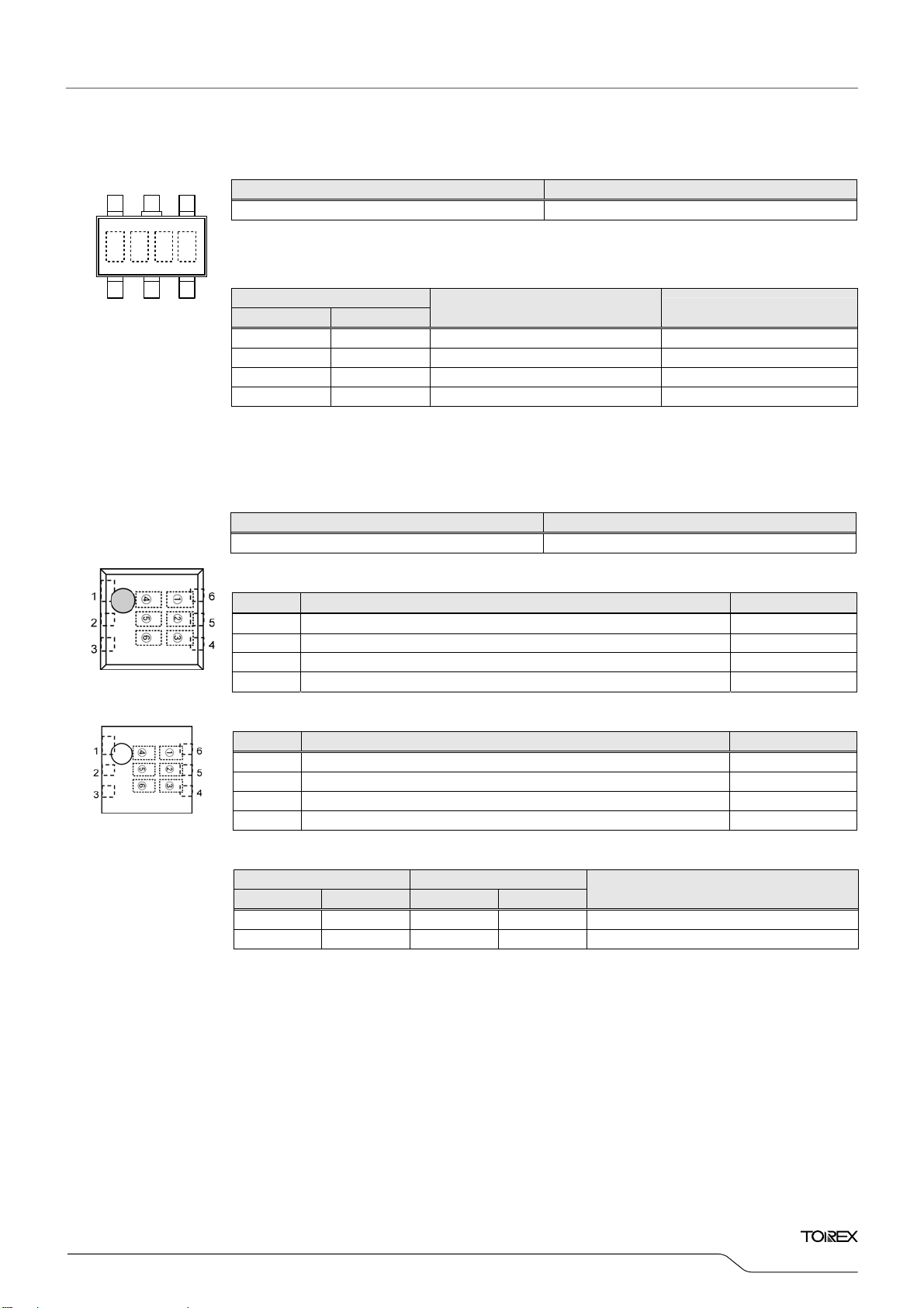
■PIN CONFIGURATION
■PIN ASSIGNMENT
SOT-26W USP-6B/C
1 3 EN1 ON/OFF Control 1
2 2 VIN Power Input
3 1 EN2 ON/OFF Control 2
4 6 VOUT2 Output 2
5 4 VSS Ground
6 5 VOUT1 Output 1
■PRODUCT CLASSIFICATION
●Selection Guide
The following options for the Regulator 1, 2, the EN pin logic, internal pull-up / down are available.
●Ordering Information
XC6401①②③④⑤⑥-⑦
DESIGNATOR DESCRIPTION SYMBOL DESCRIPTION
③④
⑤⑥-⑦
(*1)
The “-G” suffix indicates that the products are Halogen and Antimony free as well as being fully RoHS compliant.
(*2)
The device orientation is fixed in its embossed tape pocket.
For reverse orientation, please contact your local Torex sales office or representative.
(Standard orientation: ⑤R-⑦, Reverse orientation: ⑤L-⑦)
VSSVOUT1
56
12
SOT-26W
(TOP VIEW)
PIN NUMBER
①
②
VOUT2
4
3
EN2VINEN1
USP-6B /USP-6C
(BOTTOM VIEW)
PIN NAME FUNCTION
(*1)
E High Active with pull-down resistor
Regulator1,
EN type
F High Active with no pull-down resistor
G Low Active with pull-up resistor
H Low Active with no pull-up resistor
E High Active with pull-down resistor
Regulator2,
EN type
F High Active with no pull-down resistor
G Low Active with pull-up resistor
H Low Active with no pull-up resistor
Output Voltage 01~
MR SOT-26W
MR-G SOT-26W
Packages
Taping Type
(*2)
DR USP-6B
DR-G USP-6B
ER USP-6C
ER-G USP-6C
*The dissipation pad for the USP-6B/C packages
should be solder-plated in recommended mount
pattern and metal masking so as to enhance
mounting strength and heat release.
If the pad needs to be connected to other pins, it
should be connected to the V
Internally set sequential number relating output voltage of
each regulators
Regulator 1 Output Voltage Range: 0.8 ~ 5.0 V (0.05V increments)
Regulator 2 Output Voltage Range: 0.8 ~ 5.0 V (0.05V increments)
SS pin.
2/24

A
■
BSOLUTE MAXIMUM RATINGS
PARAMETER SYMBOL RATINGS UNITS
Input Voltage VIN 6.5 V
Output Current IOUT1 + IOUT2 700 mA
Output Voltage VOUT VSS -0.3 ~ VIN +0.3 V
EN Pin Voltage VEN VSS -0.3 ~ 6.5 V
SOT-26W 250
Power Dissipation
USP-6B 100
Pd
USP-6C
Operating Temperature Range Topr -40 ~ +85
Storage Temperature Range Tstg -55 ~ +125
* Sum of IOUT1 and IOUT2.
** Pd=(V
■ELECTRICAL CHARACTERISTICS
XC6401FFxx
Regulator 1, Regulator 2
IN-VOUT1)xIOUT1+(VIN-VOUT2)xIOUT2
XC6401
Series
Ta = 25℃
mW
100
℃
℃
Ta=25℃
PARAMETER SYMBOL CONDITIONS MIN. TYP. MAX. UNITS CIRCUIT
Output Voltage (*3) VOUT (E) VIN=VOUT (T) + 1.0V IOUT=30mA 0.98 VOUT(T) 1.02 V 1
Maximum Output Current IOUTMAX VIN=VOUT (T) + 1.0V 150 - - mA 1
Load Regulation △VOUT 1mA≦IOUT≦100mA - 15 60 mV 1
Dropout Voltage
Supply Current ISS
Vdif1 IOUT=30mA E-1 mV
Vdif2 I
OUT=100mA E-2 mV
IN=VEN=VOUT (T) + 1.0V,
V
I
OUT=0mA
- 25 45 μA 2
1
Standby Current ISTB VIN=VOUT (T) + 1.0V, VEN=VSS - 0.01 0.10 μA 3
Line Regulation (*7)
△VOUT VOUT(T)+1.0V≦VIN≦6.0V
△V
IN ・ VOUT VEN=VIN, IOUT=30mA
- 0.01 0.20 % / V 1
Input Voltage VIN 1.5 - 6.0 V -
Output Voltage △VOUT IOUT=30mA
- ±100 - ppm/℃ 1
Temperature Characteristics △Topr ・ VOUT -40℃≦Topr≦85℃
IN=[VOUT(T)+1.0]VDC+0.5Vp-pAC
Ripple Rejection Rate(*8) PSRR
V
IOUT=30mA, f=1kHz
- 70 - dB 5
Current Limiter Ilim VIN=VOUT (T) + 1.0V, VEN=VIN - 300 - mA 1
Short-Circuit Current Ishort VIN=VOUT (T) + 1.0V, VEN=VIN - 30 - mA 1
EN "High" Voltage VENH 1.30 - 6.0 V 4
EN "Low" Voltage VENL - - 0.25 V 4
EN "High" Current IENH VIN=VEN=VOUT (T) + 1.0V -0.10 - 0.10 μA 4
EN "Low" Current IENL VIN= VOUT (T) + 1.0V, VEN=VSS -0.10 - 0.10 μA 4
NOTE *1: VOUT(T)=Specified output voltage
*2: V
OUT(E)=Effective output voltage
(I.e. the output voltage when "V
OUT (T)≦1.45V, MIN VOUT (T) - 30mV, MAX VOUT (T) + 30mV
*3: If V
*4: Vdif={V
OUT1=A voltage equal to 98% of the output voltage whenever an amply stabilized IOUT {VOUT(T)+1.0V} is input.
*5: V
IN1=the input voltage when VOUT1 appears as input voltage is gradually decreased.
*6: V
*7: When V
*8: When V
*9: Unless otherwise stated, V
(*6)
IN1
OUT(T)>4.5V, 5.5V<VIN<6.0V
OUT(T)>4.8V, VIN=5.75VDC+0.5Vp-pAC
-VOUT1
(*5)
}
OUT(T)+1.0V" is provided at the VIN pin while maintaining a certain IOUT value).
IN=VOUT(T)+1.0V
3/24

XC6401 Series
■ELECTRICAL CHARACTERISTICS (Continued)
●Dropout Voltage
E-1 E-2
80 400 240 500
65 300 200 400
60 200 180 300
55 100 165 250
50 75 150 200
45 65 140 180
40 60 120 170
35 55 110 160
SETTING OUTPUT VOLTAGE
(V) VOUT Vdif 1 Vdif 2
VOUT(T) MIN. MAX. TYP. MAX. TYP. MAX.
0.80 0.770 0.830
0.85 0.820 0.880
0.90 0.870 0.930
0.95 0.920 0.980
1.00 0.970 1.030
1.05 1.020 1.080
1.10 1.070 1.130
1.15 1.120 1.180
1.20 1.170 1.230
1.25 1.220 1.280
1.30 1.270 1.330
1.35 1.320 1.380
1.40 1.370 1.430
1.45 1.420 1.480
1.50 1.470 1.530
1.55 1.519 1.581
1.60 1.568 1.632
1.65 1.617 1.683
1.70 1.666 1.734
1.75 1.715 1.785
1.80 1.764 1.836
1.85 1.813 1.887
1.90 1.862 1.938
1.95 1.911 1.989
2.00 1.960 2.040
2.05 2.009 2.091
2.10 2.058 2.142
2.15 2.107 2.193
2.20 2.156 2.244
2.25 2.205 2.295
2.30 2.254 2.346
2.35 2.303 2.397
2.40 2.352 2.448
2.45 2.401 2.499
2.50 2.450 2.550
2.55 2.499 2.601
2.60 2.548 2.652
2.65 2.597 2.703
2.70 2.646 2.754
2.75 2.695 2.805
2.80 2.744 2.856
2.85 2.793 2.907
2.90 2.842 2.958
2.95 2.891 3.009
DETECT VOLTAGE
(V) (mV) (mV)
DROPOUT VOLTAGE 1 DROPOUT VOLTAGE 2
300 700 400 800
200 600 350 700
100 500 270 600
4/24

■DROPOUT VOLTAGE CHART (Continued)
●Dropout Voltage (Continued)
SETTING OUTPUT VOLTAGE
(V) VOUT Vdif 1 Vdif 2
VOUT(T) MIN. MAX. TYP. MAX. TYP. MAX.
3.00 2.940 3.060
3.05 2.989 3.111
3.10 3.038 3.162
3.15 3.087 3.213
3.20 3.136 3.264
3.25 3.185 3.315
3.30 3.234 3.366
3.35 3.283 3.417
3.40 3.332 3.468
3.45 3.381 3.519
3.50 3.430 3.570
3.55 3.479 3.621
3.60 3.528 3.672
3.65 3.577 3.723
3.70 3.626 3.774
3.75 3.675 3.825
3.80 3.724 3.876
3.85 3.773 3.927
3.90 3.822 3.978
3.95 3.871 4.029
4.00 3.920 4.080
4.05 3.969 4.131
4.10 4.018 4.182
4.15 4.067 4.233
4.20 4.116 4.284
4.25 4.165 4.335
4.30 4.214 4.386
4.35 4.263 4.437
4.40 4.312 4.488
4.45 4.361 4.539
4.50 4.410 4.590
4.55 4.459 4.641
4.60 4.508 4.692
4.65 4.557 4.743
4.70 4.606 4.794
4.75 4.655 4.845
4.80 4.704 4.896
4.85 4.753 4.947
4.90 4.802 4.998
4.95 4.851 5.049
5.00 4.900 5.100
DETECT VOLTAGE
(V) (mV) (mV)
DROPOUT VOLTAGE 1 DROPOUT VOLTAGE 2
30 45 100 150
XC6401
Series
E-1 E-2
5/24

XC6401 Series
■OPERATIONAL EXPLANATION
<Output Voltage Control>
The voltage divided by resistors R1 & R2 is compared with the internal reference voltage by the error amplifier. T he
P-channel MOSFETs, which are connected to the V
signal. The output voltages at the VOUT1 and VOUT2 pins are controlled and stabilized by a system of negative
feedback. The current limit circuit and short protect circuit operate in relation to the level of output current. Further, the
IC's internal circuitry can be shutdown via the EN pin's signal.
EN1
ON/OFF
Control
VR1
each
circuit
V
IN
V
SS
EN2
VR2
each
circuit
ON/OFF
Control
Voltage
Reference
<Low ESR Capacitors>
With the XC6401 series, a stable output voltage is achievable even if used with low ESR capacitors as a phase
compensation circuit is built-in. In order to ensure the effectiveness of the phase compensation, we suggest that output
capacitors (CL1, CL2) is connected as close as possible to the output pins (V
Please use an output capacitor with a capacitance value of at least 1μF. Also, please connect an input capacitor (C
1μF between the VIN pin and the VSS pin in order to ensure a stable power input.
<Current Limiter, Short-Circuit Protection>
The XC6401 series includes a combination of a fixed current limiter circuit & a foldback circuit which aid the operations of
the current limiter and circuit protection. When the load current reaches the current limit level, the fixed current limiter
circuit operates and output voltage drops. As a result of this drop in output voltage, the foldback circuit operates, output
voltage drops further and output current decreases. When the output pin is shorted, a current of about 30mA flows.
<EN Pins>
The IC's internal circuitry can be shutdown via the signal from the EN1 and EN2 pins with the XC6401 series. In
shutdown mode, output at the V
The operational logic of the IC's EN1 and EN2 pins are selectable (please refer to the selection guid e). Note that as the
standard XC6401FF type's regulator 1 and 2 are both ' High Active/No Pull Down', operati ons will become unstable with
the EN1 or EN2 pins open. Although the EN1 and EN2 pins are equal to an inverter input with CMOS hysteresis, with
either the pull-up or pull-down options, the EN1 and EN2 pins input current will increase when the IC is in operation.
We suggest that you use this IC with either a V
used with the correct specifications for the EN1 and EN2 pins, the operational logic is fixed and the IC will operate
normally. However, supply current may increas e as a result o f through current in the IC's internal circuitry.
■NOTES ON USE
1. Please use this IC within the stated absolute maximum ratings.
The IC is liable to malfunction should the ratings be exceeded.
2. Where wiring impedance is high, operations may become unstable due to noise and/or phase lag
depending on output current. Please keep the resistance low between V
3. Please wire the input capacitor (C
OUT1 and VOUT2 pins will be pulled down to the VSS level via R11 & R12 and R21 & R22.
IN) and the output capacitors (CL1, CL2) as close to the IC as possible.
OUT1 and VOUT2 pins, are then driven by the subsequent output
-
Error
Amp1
+
-
Error
Amp2
+
IN voltage or a VSS voltage input at the EN1 and EN2 pins. If this IC is
Current
Limit
Current
Limit
OUT1
V
R11
R12
V
OUT2
R21
R22
OUT1 and VOUT2) and the VSS pin.
IN and VSS wiring in particular.
IN) of
6/24

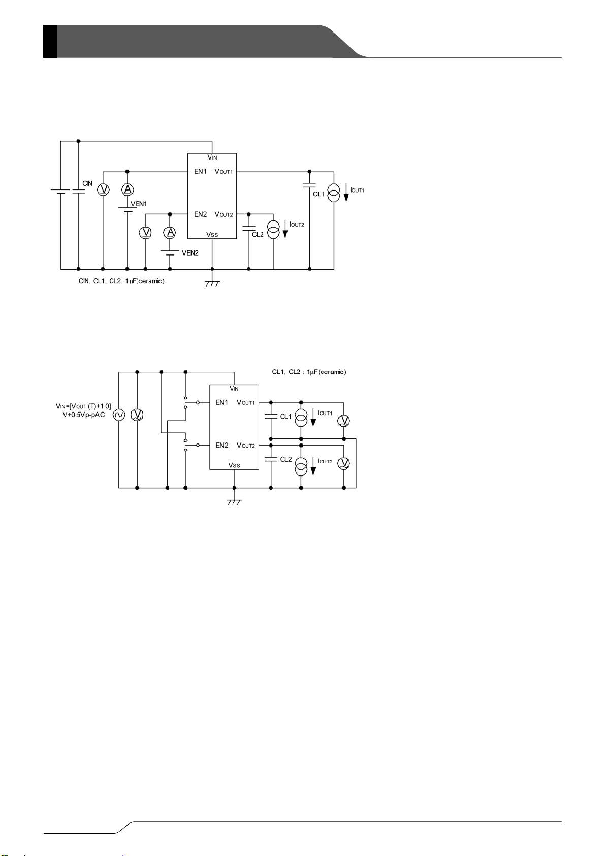
■TEST CIRCUITS
Circuit ①
V
Circuit ②
Circuit ③
CIN
EN1
EN2
CIN, CL 1 , CL2 : 1 μF(ceramic)
V
IN
V
OUT1
V
OUT2
V
SS
CL1
CL2
XC6401
Series
A
I
OUT1
V
RL1
A
I
OUT2
V
RL2
EN1/EN2 :
High Active = EN=V
Low Active = EN=V
IN
SS
EN1/EN2 :
1. High Active with pull-down resistor built-in
VR1 Supply Current I
SS1=I1 (Note:EN1=ON, EN2=OFF)
VR2 Supply Current ISS2=I1 (Note:EN1=OFF, EN2= ON)
2. High Active with no pull-down resistor built-in
VR1 Supply Active Current I
SS1=I1
(Note:EN1=ON, EN2=OFF)
VR2 Supply Current I
SS2=I1 (Note:EN1=OFF, EN2=ON)
3. Low Active with pull-up resistor built-in
VR1 Supply Current I
SS1=I1+I2
(Note:EN1=ON, EN2=OFF)
VR2 Supply Current I
SS2=I1+I3
(Note:EN1=OFF, EN2=ON)
4. Low Active with no pull-up resistor built-in
VR1 Supply Current I
VR2 Supply Current I
SS1=I1 (Note:EN1=ON, EN2=OFF)
SS2=I1 (Note:EN1=OFF, EN2=ON)
EN1/EN2:
High Active = EN= V
Low Active = EN= V
SS
IN
7/24
)
XC6401 Series
■TEST CIRCUITS (Continued
Circuit ④
Circuit ⑤
EN1/EN2 :
High Active = EN=V
Low Active = EN=V
IN
SS
8/24

)
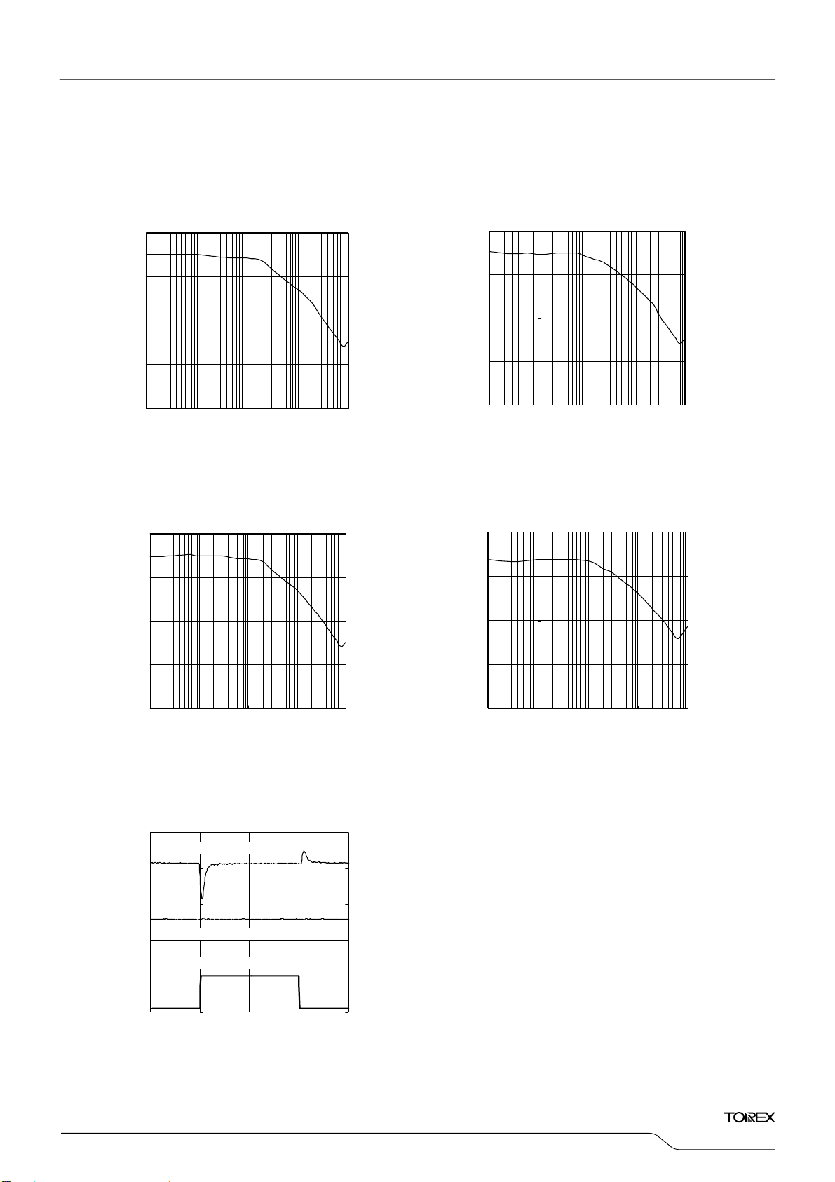
■TYPICAL PERFORMANCE CHARACTERISTICS
(1) Output Voltage vs. Output Current
1.0
XC 6401 (0.8V
VIN=1. 8V
CIN=1uF (cerami c s ), CL= 1uF (ceram ic s )
CIN=1uF (ceram ic s ), CL= 1uF (ceram ic s )
1.0
0.8
0.6
0.4
Topr = 85OC
= 25
= - 40
O
O
C
C
0.8
VIN = 6.0V
0.6
0.4
Output Volt age V OUT (V)
0.2
Output Volt age V OUT (V)
0.2
0.0
0 50 100 150 200 250 300 350
Output Current IOUT (mA)
0.0
0 50 100 150 200 250 300 350
CIN=1uF (ceramics ), CL= 1uF (ceram ic s )
4.0
3.5
3.0
2.5
2.0
1.5
1.0
Output Volt age V OUT (V)
0.5
0.0
0 50 100 150 200 250 300 350
XC 6401 ( 2 .85 V)
Topr = 85OC
O
= 25
C
O
= - 40
C
Output Current IOUT (mA)
VIN=3.85V
CIN=1uF (cerami c s ), CL= 1uF (ceram ic s )
4.0
3.5
3.0
2.5
2.0
1.5
1.0
Output Volt age V OUT (V)
0.5
0.0
VIN = 6. 0V
0 50 100 150 200 250 300 350
XC6401
Series
XC 6401 ( 0 .8V)
VIN=4.0V
= 1.8V
= 1.8V
= 1.5V
Output Current IOUT (mA)
XC 6401 ( 2 .85 V)
VIN=4. 0V
= 4.0V
= 3.15V
Output Current IOUT (mA)
XC6401(3.0V)
CIN=1uF (ceramics ), CL= 1uF (ceram ic s )
4.0
3.5
3.0
2.5
2.0
1.5
1.0
Output V ol t age V OUT (V )
0.5
0.0
Topr = 85OC
0 50 100 150 200 250 300 350
Output Current IOUT (m A)
= 25
= - 40
O
C
O
C
VIN=4.0V
CIN=1uF (ceram ic s ), CL= 1uF (ceram ic s )
4.0
3.5
3.0
2.5
2.0
1.5
1.0
Output Voltage VOUT (V)
0.5
0.0
0 50 100 150 200 250 300 350
XC 6401 (3.0V)
VIN=4.0V
VIN = 6. 0V
= 4.0V
= 3..3V
Output Current IOUT (m A)
9/24

)
XC6401 Series
■TYPICAL PERFORMANCE CHARACTERISTICS (Continued)
(1) Output Voltage vs. Output Current (Continued)
CIN=1uF (ceramic s ), CL= 1uF (c eramics )
6.0
5.0
4.0
3.0
2.0
Output Volt age V O UT (V )
1.0
0.0
0 50 100 150 200 250 300 350
(2) Output Voltage vs. Input Voltage
Output V ol tage VOUT (V )
CIN=1uF (ceramic s ), CL= 1uF (ceram ic s )
1.2
1.1
1.0
0.9
0.8
0.7
0.6
0.5
0.5 1.0 1. 5 2. 0 2.5
CIN=1uF (ceramic s ), CL= 1uF (ceram ic s )
3.05
2.85
2.65
2.45
2.25
Output Volt age V O UT (V )
2.05
2.35 2. 85 3.35
XC6401( 5.0V)
Topr = 85OC
O
C
= 25
O
= - 40
C
Output Current IOUT (mA)
XC6401(0.8V
IOUT = 0mA
= 30m A
= 100m A
Input Voltage V IN (V)
XC6401( 2.85V)
IOUT = 0mA
Input Voltage V IN (V)
VIN=6.0V
Topr = 25OC
Topr = 25OC
= 30m A
= 100mA
XC6401( 5.0V)
CIN=1uF (ceramic s ), CL= 1uF (ceram ic s )
6.0
5.0
4.0
3.0
2.0
Output Volt age V O UT (V )
1.0
0.0
0 50 100 150 200 250 300 350
VIN = 6.0V
= 5.3V
Output Current IOUT (mA)
VIN=4.0V
XC6401( 0.8V)
CIN=1uF (ceramic s ), CL= 1uF (c eramic s)
0.90
0.85
0.80
0.75
Output V ol tage VOUT (V )
0.70
0.65
1.5 2.0 2.5 3.0 3.5 4. 0 4. 5 5.0 5.5 6.0
Input Voltage V IN (V)
Topr = 25OC
IOUT = 0mA
= 30mA
= 100mA
XC6401( 2 .85V)
CIN=1uF (ceramic s ), CL= 1uF (ceram ic s )
2.95
2.90
2.85
2.80
2.75
Output Volt age V O UT (V )
2.70
3.0 3.5 4.0 4.5 5.0 5.5 6.0
Input Voltage V IN (V)
Topr = 25OC
IOUT = 0mA
= 30m A
= 100mA
10/24

■TYPICAL PERFORMANCE CHARACTERISTICS (Continued)
(2) Output Voltage vs. Input Voltage (Continued)
CIN=1uF (ceramics ), CL=1uF (ceram ic s )
3.2
3.0
2.8
2.6
Output V ol tage VOUT (V )
2.4
XC6401(3.0V)
IOUT = 0mA
Top r = 2 5
= 30mA
= 100m A
O
C
Output Volt age VOUT (V)
CIN=1uF (ceram ics ), CL= 1uF (c erami c s )
3.10
3.05
3.00
2.95
2.90
XC6401(3.0V)
IOUT = 0mA
= 30mA
= 100m A
2.2
2.5 3.0 3.5
Input Volt age V IN (V)
2.85
3.5 4.0 4. 5 5.0 5.5 6.0
Input Volt age VIN (V)
5.2
XC6401(5.0V)
Topr = 25OC
CIN=1uF (ceramics ), CL= 1uF (ceram ics )
5.10
CIN=1uF (ceramics ), CL=1uF (ceram ic s )
XC6401(5.0V)
5.0
5.05
4.8
4.6
IOUT = 0mA
= 30mA
= 100m A
5.00
4.95
IOUT = 0mA
= 30mA
= 100mA
4.4
Output Voltage VOUT (V)
Output V ol tage VOUT (V )
4.90
(3) Dropout Voltage vs. Output Current
4.2
4.5 5.0 5.5
Input Volt age V IN (V)
XC6401(0.8V)
CIN=1uF (ceramics ), CL=1uF (ceram ic s )
1.0
0.8
Top r = 85OC
0.6
= 25
= - 40
O
C
O
C
4.85
5.5 6.0
Input Voltage VIN (V)
XC6401(2.85V)
CIN=1uF (ceramics ), CL= 1uF (ceram ic s )
0.5
0.4
Topr = 85OC
0.3
0.4
0.2
Dropout Vol tage Vdif (V)
0.2
Dropout Voltage Vdi f (V)
0.1
0.0
0 50 100 150 200
Output Current IOUT (m A)
0.0
0 50 100 15 0 200
Output Current IOUT (mA)
Top r = 2 5OC
Top r = 2 5OC
O
= 25
C
O
C
= - 40
XC6401
Series
11/24

XC6401 Series
■TYPICAL PERFORMANCE CHARACTERISTICS (Continued)
(3) Dropout Voltage vs. Output Current (Continued)
XC6401(3.0V)
CIN=1uF (ceramic s ), CL= 1uF (c eramics )
0.5
0.4
0.3
0.2
Dropout Voltage V di f (V )
0.1
0.0
0 50 100 150 200
Output Current IOUT (mA)
Topr = 85OC
(4) Supply Current vs. Input Voltage
XC6401(0.8V)
100
80
60
Topr = 85OC
= 25
= - 40
= 25
= - 40
XC6401(5.0V)
CIN=1uF (ceramic s ), CL= 1uF (c eramic s )
0.5
O
C
O
C
0.4
0.3
0.2
Dropout V ol tage V di f (V)
0.1
0.0
0 50 100 150 200
Output Current IOUT (mA)
Topr = 85OC
= 25
= - 40
O
C
O
C
XC6401(2.85V)
100
O
C
O
C
80
60
Topr = 8 5OC
= 25
= - 40
O
C
O
C
40
Supply Current ISS (uA)
20
0
0123456
Input Voltage V IN (V)
XC6401(3.0V)
100
80
60
40
Supply Current ISS (uA)
20
0
0123456
Input Voltage V IN (V)
Topr = 85OC
= 25
= - 40
O
C
O
C
40
Supply Current ISS (uA)
20
0
0123456
Intput Voltage V IN (V)
XC6401(5.0V)
100
80
60
40
Supply Current ISS (uA)
20
0
0123456
Topr = 8 5OC
= 25
= - 40
Input Voltage VIN (V)
O
C
O
C
12/24

X
V
)
■TYPICAL PERFORMANCE CHARACTERISTICS (Continued)
(5) Output Voltage vs. Ambient Temperature
XC6401
Series
XC6401(0.8V)
CIN=1uF (ceram ics ), CL=1uF (c eram ic s)
0.84
0.82
0.80
IOUT = 0mA
= 10mA
0.78
Output V oltage V OUT (V)
0.76
-50-25 0 25 50 75100
Am bient Temperat ure Topr (
= 30mA
= 100mA
VIN = 1. 8V
O
C)
CIN=1uF (ceram ic s), CL= 1u F (c eram ic s)
2.95
2.90
2.85
2.80
Output V oltage V OUT (V)
2.75
-50-250255075100
XC6401(3.0V)
CIN=1uF (ceram ics ), CL= 1uF (c eram ic s)
3.10
3.05
VIN = 4.0V
CIN=1uF (ceram ic s ), CL=1uF (c eram ic s )
5.20
5.10
XC6401(2.85V)
IOUT = 0mA
= 10mA
= 30mA
= 100m A
Am bient Temperature Topr (
C6401(5.0
VIN = 4.0V
O
C)
VIN = 5.0V
3.00
2.95
Output Volt age VOUT (V)
2.90
-50-25 0 25 50 75100
IOUT = 0mA
= 10mA
= 30mA
= 100m A
Am bient Temperat ure Topr (
(6) Supply Current vs. Ambient Temperature
XC6401(0.8V)
30
28
A)
μ
26
24
Supply Current IDD (
22
20
-50-250 255075100
Ambient Temperature Topr (
VIN = 1.8V
5.00
4.90
Output V oltage V OUT (V)
4.80
O
C)
-50-250255075100
IOUT = 0mA
= 10m A
= 30m A
= 100mA
Am bient Temperature Topr (
O
C)
XC6401(2.85V)
30
28
A)
μ
26
24
Supply Current IDD (
22
20
O
C)
-50-250 255075100
Ambient Temperature Topr (
VIN = 3.85V
O
C)
13/24

XC6401 Series
■TYPICAL PERFORMANCE CHARACTERISTICS (Continued)
(6) Supply Current vs. Ambient Temperature (Continued)
XC6401(3.0V)
30
28
A)
μ
26
24
Supply Current I DD (
22
20
-50-250 255075100
Ambient Temperature Topr (
VIN = 4.0V
XC6401(5.0V)
VIN = 6. 0V
30
28
A)
μ
26
24
Supply Current I DD (
22
20
O
C)
-50 -25 0 25 50 75 100
Am bient Temperature Topr (
O
C)
14/24

■TYPICAL PERFORMANCE CHARACTERISTICS (Continued)
(7) Input Transient Response
XC6401
Series
Output V ol t age V OUT (V )
1.00
0.95
0.90
0.85
0.80
0.75
0.70
1.00
0.95
0.90
XC 6401(0.8V)
tr=t f=5use
CL=1uF (c eram ic s ), IOUT=100uA
Input Voltage
Output Voltage
Time (200usec / div)
XC 6401(0.8V)
tr=t f=5use
CL=1uF (c eram ic s ), IOUT=100mA
Input Voltage
XC6401(0.8V)
4
3
2
1
0
Input Voltage VIN (V)
-1
-2
1.00
0.95
0.90
0.85
0.80
Output Vol tage V OUT (V )
0.75
0.70
CL=1uF (c eram ic s ), IOUT=30mA
Input Voltage
Output Voltage
Time (40usec / div)
tr=t f=5use
4
3
2
1
0
Input V ol t age V IN (V)
-1
-2
XC6401(2.85V)
4
3
2
3.05
3.00
2.95
CL=1uF (c eram ic s ), IOUT=100uA
Input Voltage
tr=t f=5use
6
5
4
Output Vol tage V OUT (V )
Output V ol t age V OUT (V )
0.85
0.80
0.75
0.70
3.05
3.00
2.95
2.90
2.85
2.80
2.75
Output Voltage
Time (40usec /div)
XC 64 01 (2.85V)
tr=t f=5use
CL=1uF (c eram ic s ), IOUT=30mA
Input Voltage
Output V olt age
Time (40usec / div)
1
0
Input Voltage VIN (V)
-1
-2
2.90
2.85
Output Vol tage V OUT (V )
2.80
2.75
Output Voltage
Time (200usec /di v)
3
2
Input V ol t age V IN (V)
1
0
XC6401(2.85V)
6
5
4
3
2
Input V o l tage VIN (V)
1
0
3.05
3.00
2.95
2.90
2.85
Output V ol t age V OUT (V )
2.80
2.75
CL=1uF (c erami cs ), IOUT=100mA
Input Voltage
Output Voltage
Time (40usec/div)
tr=tf=5use
6
5
4
3
2
Input Voltage VIN (V)
1
0
15/24

XC6401 Series
■TYPICAL PERFORMANCE CHARACTERISTICS (Continued)
(7) Input Transient Response (Continued)
Output Vol tage V OUT (V)
3.20
3.15
3.10
3.20
3.15
3.10
3.05
3.00
2.95
2.90
XC6401(3.0V)
tr=tf= 5use
CL=1uF (c erami c s ), IOUT=100uA
Input Voltage
Output Voltage
Time (200usec /d iv)
XC6401(3.0V)
tr=tf= 5use
CL=1uF (ceram ic s ), IOUT=100m A
Input Voltage
XC6401(3.0V)
6
5
4
3
2
Input Voltage VIN (V)
1
0
3.20
3.15
3.10
3.05
3.00
Input Voltage VIN (V)
2.95
2.90
CL=1uF (c erami c s ), IOUT=30m A
Input Voltage
Output Voltage
Time (40usec /d iv)
tr=t f= 5use
6
5
4
3
2
Input Voltage VIN (V)
1
0
XC6401(5.0V)
6
5
4
5.20
5.15
5.10
CL=1uF (ceram ic s ), IOUT=100uA
Input Voltage
tr=tf= 5use
8
7
6
Output Volt ag e VOUT (V)
Output Voltage VOUT (V)
3.05
3.00
2.95
2.90
5.20
5.15
5.10
5.05
5.00
4.95
4.90
Output V o ltage
Time (40usec/div)
XC6401(5.0V)
tr=tf= 5use
CL=1uF (c eram ic s ), IOUT=30m A
Input Voltage
Output Voltage
Time (40usec/div)
3
2
Input Voltage VIN (V)
1
0
5.05
5.00
Output Voltage VOUT (V)
4.95
4.90
Output Voltage
Time (200usec / div)
5
4
Input Voltage VIN (V)
3
2
XC6401(5.0V)
8
7
6
5
4
Input Voltage VIN (V)
3
2
Output Vol tage V OUT (V)
5.20
5.15
5.10
5.05
5.00
4.95
4.90
CL=1uF (ceram ic s ), IOUT=100m A
Input Voltage
Output Voltage
Time (40usec /di v)
tr=tf= 5use
8
7
6
5
4
Input Voltage VIN (V)
3
2
16/24

■TYPICAL PERFORMANCE CHARACTERISTICS (Continued)
(8) Load Transient Response
0.90
XC 6401( 0 .8V)
VIN=1.8V , tr= tf=5us e
CIN=CL=1uF (c eramics )
250
0.90
XC6 401(0.8V)
VIN=1.8V , tr= tf=5use
CIN=CL=1uF (c eramic s )
0.80
0.70
Output V olt age
200
150
0.80
Output V olt age
0.70
XC6401
Series
250
200
150
0.60
Output Volt ag e V OUT (V)
0.50
0.40
50mA
10mA
Output Current
Time (40usec/ div)
100
50
0
0.60
Output Current IOUT (mA)
Output Vol tage VO UT (V )
0.50
0.40
XC 6401(2.85V)
VIN=4.0V , tr= tf=5us e
2.95
2.85
2.75
2.65
2.55
Output Voltage VOUT (V)
2.45
50mA
10mA
CIN=CL=1uF (c eramics )
Output V olt age
Output Current
Time (40usec/ div)
250
200
150
100
50
0
2.95
2.85
2.75
2.65
2.55
Output Current I OUT (m A)
Output Vol tage VO UT (V )
2.45
100mA
10mA
100mA
10mA
Output Current
Time (40usec/ div)
XC 6401(2.85V)
VIN=4.0V , tr= tf= 5us e
CIN=CL=1uF (c eramic s )
Output V olt age
Output Current
Time (40usec/div)
100
50
0
250
200
150
100
50
0
Output Current IOUT (mA)
Output Current IOUT (mA)
XC6 401(3.0V)
VIN=4.0V , t r= tf=5us e
3.10
3.00
2.90
2.80
50mA
Output Volt age VOUT (V)
2.70
2.60
10mA
CIN=CL=1uF (ceram ic s )
Output V olt age
Output Current
Time (40usec/ div)
250
200
150
100
50
0
Output Current IOUT (mA)
Output Volt age V OUT (V)
3.10
3.00
2.90
100mA
2.80
2.70
10mA
2.60
XC 6401( 3 .0V)
VIN=4.0V , tr= tf= 5us e
CIN=CL=1uF (c eramic s )
Output Voltage
Output Current
Time (40usec/ div)
250
200
150
100
50
0
Output Current IOUT (mA)
17/24

XC6401 Series
■TYPICAL PERFORMANCE CHARACTERISTICS (Continued)
(8) Load Transient Response (Continued)
5.10
XC6401( 5.0V)
VIN=6. 0V , tr= t f=5us e
CIN=CL=1uF (ceramic s )
250
5.10
XC6401(5.0V)
VIN=6. 0V , t r= t f=5us e
CIN=CL=1uF (c eram ic s )
250
5.00
Output V olt ag e
4.90
4.80
Output V ol t age VOUT (V)
4.70
4.60
50mA
10mA
Output Current
Time (40usec/div)
200
150
100
50
0
Output Current IOUT (mA)
5.00
Output V oltage
4.90
100mA
4.80
Output V ol t age VOUT (V)
4.70
10mA
4.60
Output Current
Time (40usec/div)
200
150
100
50
0
Output Current IOUT (mA)
18/24
■TYPICAL PERFORMANCE CHARACTERISTICS (Continued)
(9) Ripple Rejection Rate
80
XC 64 01(0.8V)
VIN=1.8V DC+ 0.5Vp-pAC
IOUT=30mA, CL= 1uF (c eram ic s )
XC 64 01 (2.85V)
VIN=3.85V DC+ 0.5Vp-pAC
80
IOUT=30mA, CL= 1uF (c eram ic s )
60
60
40
40
20
Ripple Rejec tion Rate RR (dB)
0
0.01 0.1 1 10 100
Ripple Frequency f (kHz )
20
Ripple Rej ection Ra te RR (dB)
0
0.01 0.1 1 10 100
Ripple Frequenc y f (kHz )
80
XC6401(3.0V)
VIN=4.0V DC+ 0.5Vp-pAC
IOUT=30mA, CL= 1uF (c eram ic s )
XC 64 01(5.0V)
VIN=5.75V DC+ 0.5Vp-pAC
80
IOUT=30mA, CL= 1uF (c eram ic s )
60
60
40
40
20
Ripple Rej ection Ra te RR (dB)
0
0.01 0.1 1 10 100
Ripple Frequency f (kHz )
20
Ripple Rej e ct ion Rate RR (dB)
0
0.01 0.1 1 10 100
Ripple Frequenc y f (kHz )
(10) Cross Talk
XC6401 (VR1:3.0V, VR2:2.85V)
3.1
3.0
2.9
2.8
Output Volt age VOUT (V)
2.7
2.6
VIN=4.0V, CIN= CL=1uF (c eram ic s )
VR1 Output Voltage (3.0V)
V R2 Output Voltage (2.85V )
100mA
10mA
V R1 Output Current
Time ( 4 0 u sec/d i v)
500
400
300
200
100
0
Output Current 1 I OUT (mA )
XC6401
Series
19/24
XC6401 Series
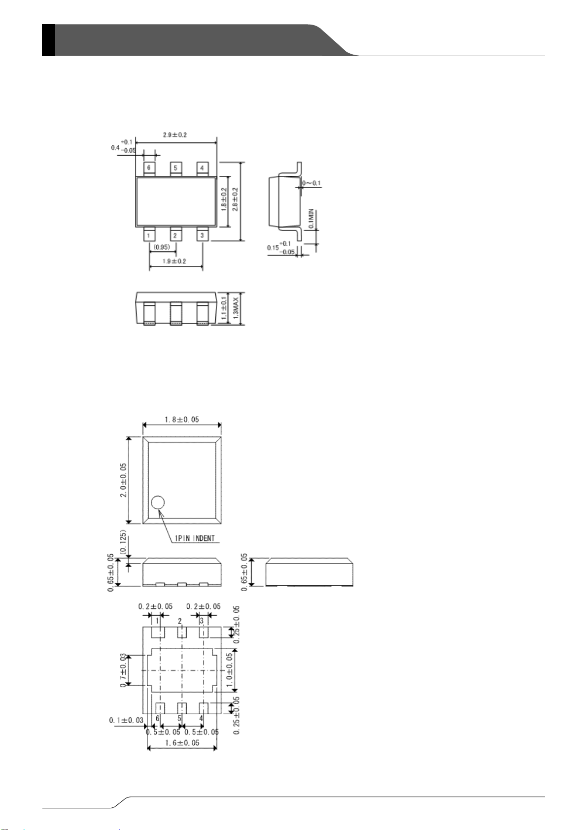
■PACKAGING INFORMATION
●SOT-26W
●USP-6B
Unit : mm
20/24
Unit : mm

■PACKAGING INFORMATION (Continued)
●USP-6C
2.0±0.05
0.6MAX
1.0±0.1
0.70±0.05
0.10±0.05
1.8±0.05
0.30±0.05
0.50
1.4±0.1
1pin INDENT
(0.10)
0.25±0.05
0.20±0.05
Unit : mm
XC6401
Series
21/24
XC6401 Series
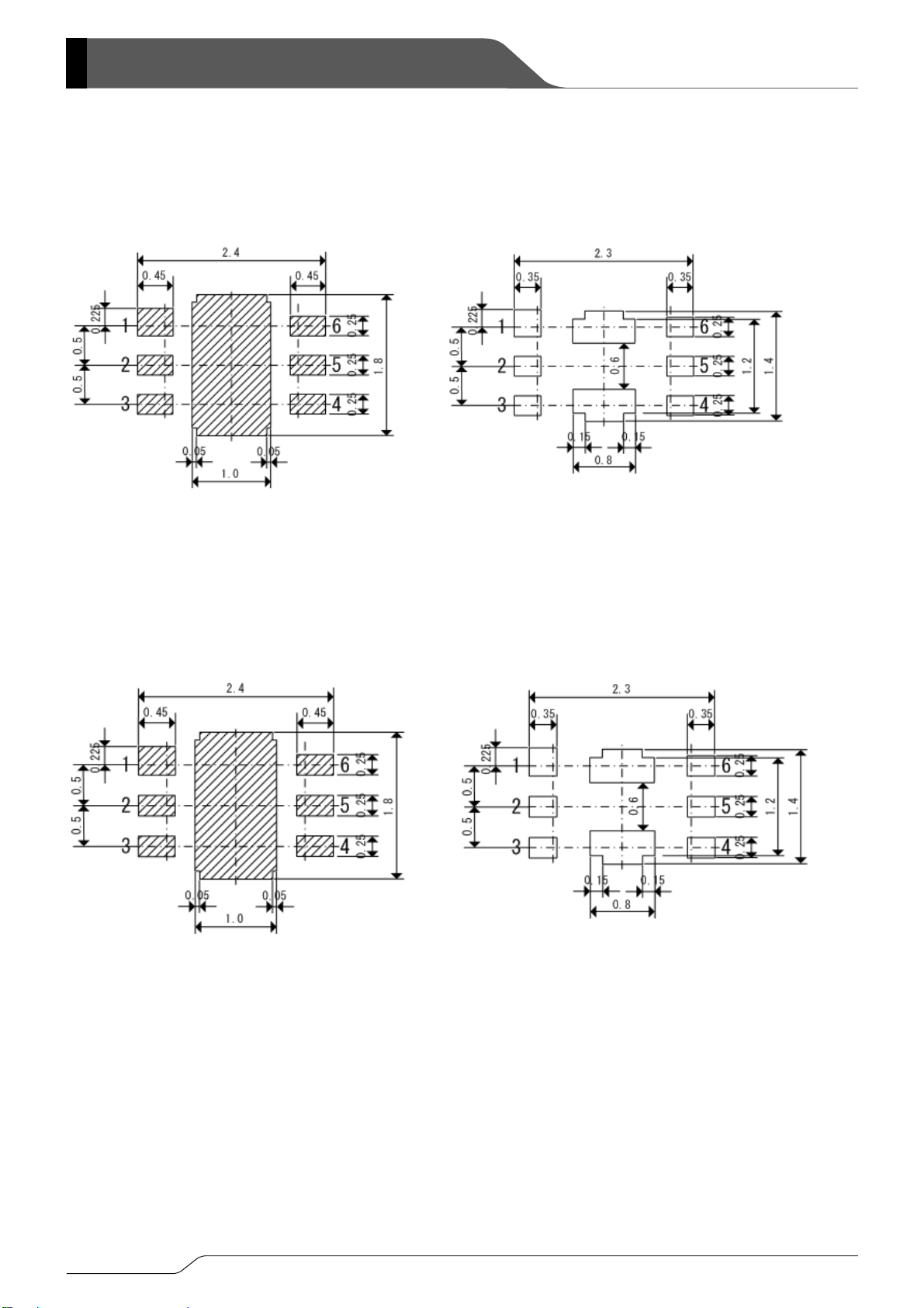
■PACKAGING INFORMATION (Continued)
●USP-6B Reference Pattern Layout
●USP-6C Reference Pattern Layout ●USP-6C Reference Metal Mask Design
●USP-6B Reference Metal Mask Design
22/24
■MARKING RULE
●SOT-26W
654
① ② ③ ④
123
SOT-26W
(TOP VIEW)
●USP-6B,USP-6C
USP-6B
(TOP VIEW)
USP-6C
(TOP VIEW)
① represents product series
②③ represents internally set sequential number
ex.)
④ represents production lot number
① represents product series
② represents type of VR1 reg ulator
③ represents type of VR2 reg ulator
④⑤ represents VR output voltage (serial number ex.)
⑥ represents production lot number
XC6401
Series
MARK PRODUCT SERIES
1 XC6401xxxxMx
MARK
② ③
C 2 C2 XC6401EED5
C 0 C0 XC6401EED6
0 1 01 XC6401FF36
1 8 18 XC6401FF37
0 to 9, A to Z reverse character 0 to 9, A to A repeated (G, I, J, O, Q, W excluded).
MARK PRODUCT SERIES
1 XC6401xxxxxx
MARK OPTIONAL FUNCTIONS PRODUCT SERIES
E EN1: High Active with pull-down resistor XC6401Exxxxx
F EN1: High Active with no pull-down resistor XC6401Fxxxxx
Z EN1: Low Active with pull-up resistor XC6401Gxxxxx
H EN1: Low Active with no pull-up resistor XC6401Hxxxxx
MARK OPTIONAL FUNCTIONS PRODUCT SERIES
E EN1: High Active with pull-down resistor XC6401xExxxx
F EN1: High Active with no pull-down resistor XC6401xFxxxx
Z EN1: Low Active with pull-up resistor XC6401xGxxxx
H EN1: Low Active with no pull-up resistor XC6401xHxxxx
MARK OUTPUT VOLTAGE
④ ⑤ VR1 (V) VR2 (V)
0 1 2.85 2.10 XC6401xx01xx
0 2 2.85 2.85 XC6401xx02xx
0 to 9, A to Z repeated (G, I, J, O, Q, W excluded)
Note: No character inversion used
INTERNALLY SET SEQUENTIAL
NUMBER
PRODUCT SERIES
PRODUCT SERIES
23/24
XC6401 Series
1. The products and product specification s containe d herein are subject to change without
notice to improve performance characteristics. Consult us, or our representatives
before use, to confirm that the information in this datasheet is up to date.
2. We assume no responsibility for any infringement of patents, patent rights, or other
rights arising from the use of any information and circuitry in this datasheet.
3. Please ensure suitable shipping controls (including fail-safe designs and aging
protection) are in force for equipment employing products listed in this datasheet.
4. The products in this datasheet are not developed, designed, or approved for use with
such equipment whose failure of malfunction can be reasonably expected to directly
endanger the life of, or cause significant injury to, the user.
(e.g. Atomic energy; aerospace; transport; combustion and associated safety
equipment thereof.)
5. Please use the prod ucts listed in this datasheet within the specified ranges.
Should you wish to use the products under conditions exceeding the specifications,
please consult us or our representatives.
6. We assume no responsibility for damage or loss due to abnormal use.
7. All rights reserved. No part of this datasheet may be copied or reproduced without the
prior permission of TOREX SEMICONDUCTOR LTD.
24/24
 Loading...