

TOREX XC6365, XC6366 User Manual
XC6365/XC6366 Series
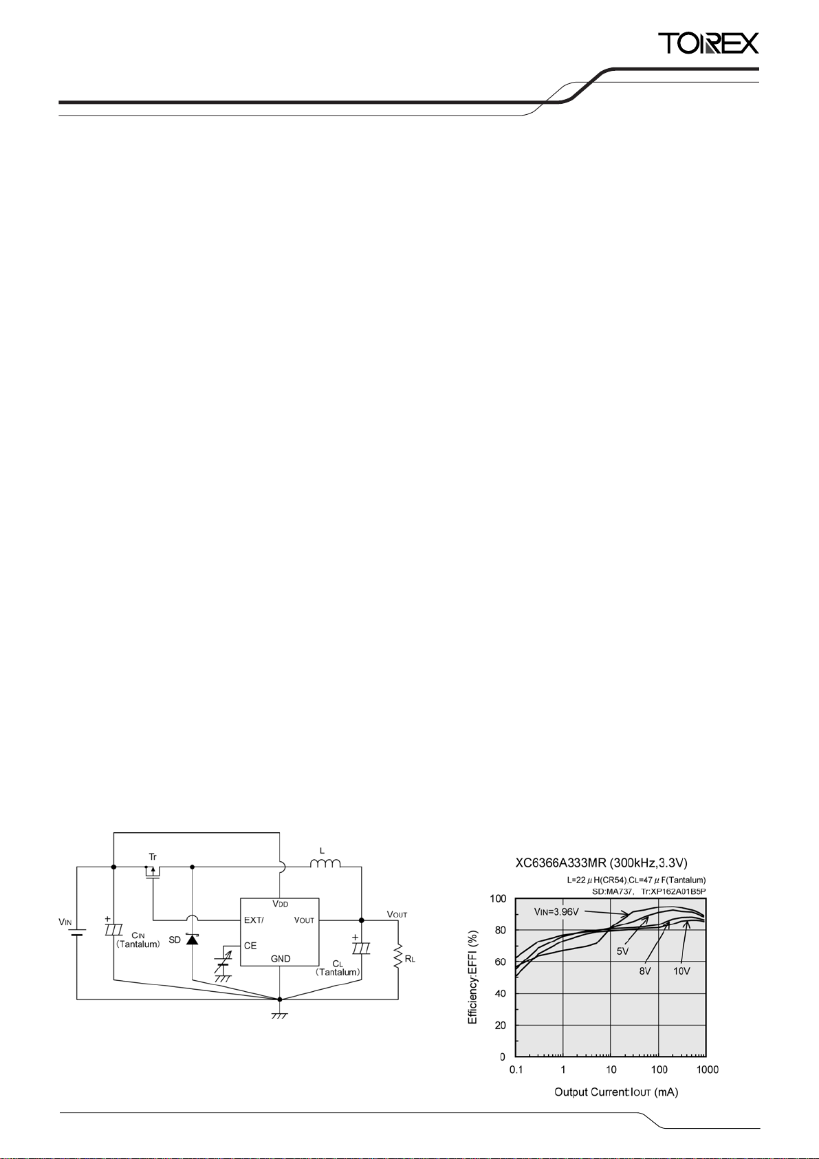
ETR0501_005a
PWM Controlled, PWM/PFM Switchable Step-Down DC/DC Controllers
■GENERAL DESCRIPTION
The XC6365/XC6366 series are multi-functional step-down DC/DC controllers which have 1A output current capability by
using an externally connected transistor, coil, diode and capacitor.
Output voltage is programmable in 0.1V increments between 1.5V to 6.0V (V
standard voltage supply internal and using externally connected components, output voltage can be set up freely (FB). With
a 300kHz switching frequency, the size of the external components can be reduced.
Control switches from PWM to PFM during light loads with the XC6366 (PWM/PFM switchable) and the series is highly
efficient from light loads to large output currents.
Soft start time of XC6365/ XC6366A, B series is internally set to 10ms and XC6365/66C, D series regulate soft-start time by
connecting resistors and capacitors externally.
During stand-by time (CE pin "Low" ), current consumption is reduced to less than 0.5μA.
With UVLO internal, the external transistor will be forcibly switched off if used below the stipulated voltage.
■APPLICATIONS
●Electronic information organizers
●Palmtops
●Cellular and portable phones
●Portable audio systems
●Various multi-function power supplies
■TYPICAL APPLICATION CIRCUIT
■FEATURES
Input Voltage Range : 2.2V ~ 10V (VOUT type)
Output Voltage Range
Oscillation Frequency
Output Current : More than 1.0A (V
High Efficiency : 92% (TYP.)
Stand-by Capability : I
Selection : Soft-start set-up external
Maximum Duty Cycle : 100%
Packages : SOT-25, USP-6C
Environmentally Friendly :
■TYPICAL PERFORMANCE
CHARACTERISTICS
OUT) (±2.5% accuracy). Further, with 1.0V of
☆GreenOperation Compatible
: 1.5V ~ 6.0V (0.1V increments) (±2.5%)
: 300kHz (±15%)
Custom products for 180, 500kHz
IN=5.0V, VOUT=3.0V)
=0.5μA (MAX.)
STB
Output voltage set-up internal (V
Output voltage set-up external (FB)
PWM/PFM Control (XC6366)
EU RoHS Compliant, Pb Free
OUT)
1/24
XC6365/XC6366 Series
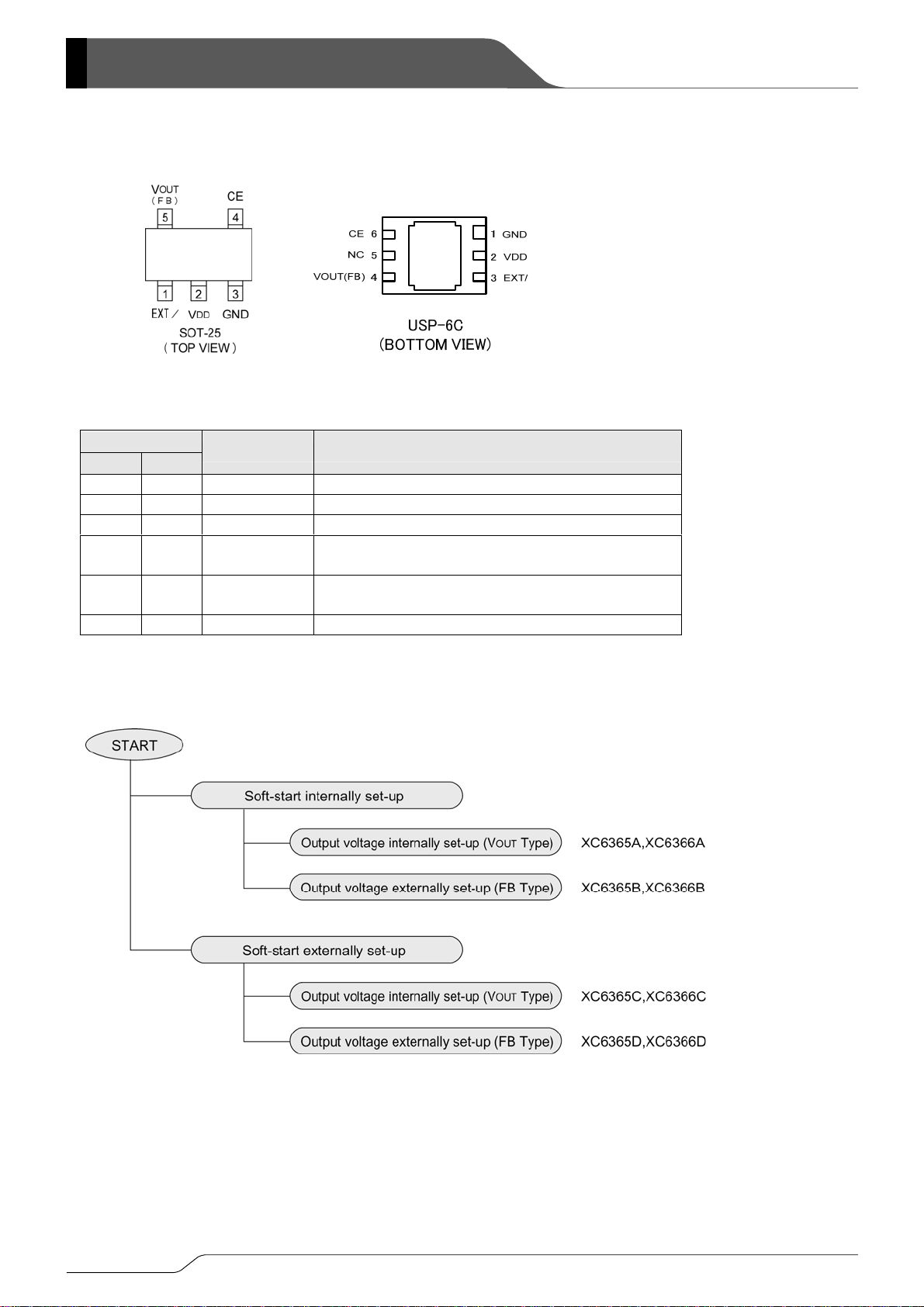
■PIN CONFIGURATION
■PIN ASSIGNMENT
PIN NUMBER
SOT-25
USP-6
PIN NAME FUNCTION
1 3 EXT/ External Transistor Connection
2 2 VDD Power Supply
3 1 GND Ground
4 6 CE
5 4 VOUT (FB)
-
■PRODUCT CLASSIFICATION
●Selection Guide
5 NC No Connection
Chip Enable Soft-Start Capacitor Connection
with Soft-Start Externally Set-Up Types (C, D)
Output Voltage Monitor FB with Externally
Set-Up Types (B, D)
*The dissipation pad of the USP-6C package
should be left open. If the circuit needs to be
connected to other pin, it should be connected to
the V
DD (No.2) pin.
2/24

■PRODUCT CLASSIFICATION (Continued)
●Ordering Information
XC6365①②③④⑤⑥-⑦
XC6366①②③④⑤⑥-⑦
(*1)
PWM control
(*1)
PWM/PFM switching control
DESIGNATOR ITEM SYMBOL DESCRIPTION
A VOUT type: Internally set-up, soft-start internally set-up
①
Type of DC/DC Converter
B FB type: Externally set-up, soft-start internally set-up
C VOUT type: Internally set-up, soft-start externally set-up
D FB type: Externally set-up, soft-start internally set-up
②③
Output Voltage
15~60 VOUT type: 3.0V output → ②=3, ③=0
10
FB type: 10 fixed → ②=1, ③=0 fixed
3 300kHz
④
Oscillation Frequency
5 500kHz (custom)
2 180kHz (custom)
MR SOT-25 (3,000/Reel)
⑤⑥-⑦
Packages
(Order Unit)
MR-G SOT-25 (3,000/Reel)
ER USP-6C (3,000/Reel)
ER-G USP-6C (3,000/Reel)
(*1)
The “-G” suffix indicates that the products are Halogen and Antimony free as well as being fully RoHS compliant.
XC6365/XC6366
Series
3/24
XC6365/XC6366 Series
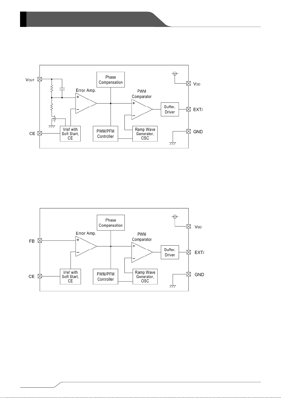
■BLOCK DIAGRAMS
XC6365, XC6366 Series A, C type (VOUT)
XC6365, XC6366 Series B, D type (FB)
4/24
XC6365/XC6366
Series
■ABSOLUTE MAXIMUM RATINGS
PAR AMETER SYMBOL RATINGS UNITS
VIN Pin Voltage VDD -0.3 ~ +12 V
VOUT Pin Voltage VOUT -0.3 ~ VIN +0.3 V
FB Pin Voltage VFB -0.3 ~ VIN +0.3 V
CE Pin Voltage VCE -0.3 ~ VIN +0.3 V
EXT/ Pin Voltage VEXT/ -0.3 ~ VIN +0.3 V
EXT/ Pin Current
Power Dissipation
SOT-25 150
USP-6C
IEXT/
Pd
±100
100
Operating Temperature Range Topr -30 ~ +80
Storage Temperature Range Tstg -40 ~ +125
Note: Voltage is all ground standardized.
■ELECTRICAL CHARACTERISTICS
XC6365A333MR, XC6366A333MR
(VOUT=3.3V, f
=300kHz)
OSC
PAR AMETER SYMBOL CONDITIONS MIN. TYP. MAX. UNITS
Output Voltage VOUT 3.218 3.300 3.383 V
Maximum Input Voltage VIN 10.0 - - V
UVLO Voltage
(Minimum Operating
Voltage)
V
UVLO
Same as I
Voltage which EXT/pin voltage holding “H” level
DD1,
0.9 - 2.2 V
Supply Current 1 IDD1 No external components, CE=VDD, VOUT=0V - 57 102
Supply Current 2 IDD2
No external components,
CE=V
OUT=VDD
XC6365 - 57 102
XC6366 - 15 27
Stand-by Current ISTB No external components, CE=VOUT=0V - - 0.5
Oscillation Frequency f
OSC
Measuring of EXT/ waveform,
VIN=output voltage + 0.1V
255 300 345 kHz
Maximum Duty Ratio MAXDTY 100 - - %
PFM Duty Ratio PFMDTY No load (XC6366 only) 15 25 35 %
CE "High" Voltage VCEH
CE "Low" Voltage VCEL
No external components, V
Voltage which EXT/pin voltage holding “L” level
No external components, V
Voltage which EXT/pin voltage holding “H” level
OUT=0V,
OUT=0V,
0.65 - - V
- - 0.20 V
EXT "High" ON Resistance REXTBH Same as IDD2, VEXT/=VDD-0.4V - 16 22
EXT "Low" ON Resistance REXTBL Same as IDD1, VEXT/=0.4V - 14 19
Efficiency EFFI
Soft-Start Time tSS
Conditions: 1. Unless otherwise stated, connect external components. VIN=VDD = 5.0V, IOUT = 220mA
2. XC6365/66C series external components: C
Use of a XP162A12A6 transistor
recommended
Connect R
(When V
SS, CSS, CE, 0V→ 3.0V
IN≦3.0V, VIN=3.0V)
SS=0.033μF, R SS=470kΩ
- 92 - %
5 10 20
Ta = 2 5℃
mA
mW
℃
℃
Ta =2 5℃
μA
μA
μA
μA
μA
μA
ms
5/24
XC6365/XC6366 Series
■ELECTRICAL CHARACTERISTICS (Continued)
XC6365A503MR, XC6366A503MR
PAR AMETER SYMBOL CONDITIONS MIN. TYP. MAX. UNITS
Output Voltage VOUT 4.875 5.000 5.125 V
Maximum Input Voltage VIN 10.0 - - V
UVLO Voltage
(Minimum Operating Voltage)
VUVLO
Same as IDD1,
Voltage which EXT/pin voltage holding “H” level
Supply Current 1 IDD1 No external components, CE=VDD, VOUT=0V - 67 122
Supply Current 2 IDD2
No external components,
CE=V
OUT=VDD
Stand-by Current ISTB No external components, CE=VOUT=0V - - 0.5
Oscillation Frequency f
OSC
Measuring of EXT/ waveform,
V
IN=output voltage + 0.1V
Maximum Duty Ratio MAXDTY 100 - - %
PFM Duty Ratio PFMDTY No load (XC6366 only) 15 25 35 %
CE "High" Voltage VCEH
CE "Low" Voltage VCEL
No external components, VOUT=0V,
Voltage which EXT/pin voltage holding “L” level
No external components, VOUT=0V,
Voltage which EXT/pin voltage holding “H” level
EXT "High" ON Resistance REXTBH Same as IDD2, VEXT/=VIN-0.4V - 12 17
EXT "Low" ON Resistance REXTBL Same as IDD1, VEXT/=0.4V - 10 14
Efficiency EFFI
Soft-Start Time tSS
Conditions: 1. Unless otherwise stated, connect external components. VIN=VDD = 7.5V, IOUT = 330mA
2. XC6365/66C series external components: C
Use of a XP162A12A6
transistor recommended
Connect R
(When V
SS, CSS, CE, 0V→ 3.0V
IN≦3.0V, VIN=3.0V)
SS=0.033μF, R SS=470kΩ
(VOUT=5.0V, f
XC6365 - 67 122
XC6366 - 16 29
=300kHz)
OSC
Ta =2 5℃
0.9 - 2.2 V
μA
μA
μA
μA
255 300 345 kHz
0.65 - - V
- - 0.20 V
μA
μA
- 93 - %
5 10 20 ms
6/24
XC6365/XC6366
Series
■ELECTRICAL CHARACTERISTICS (Continued)
XC6365B103MR, XC6366B103MR
PAR AMETER SYMBOL CONDITIONS MIN. TYP. MAX. UNITS
Output Voltage VOUT 2.925 3.000 3.075 V
Maximum Input Voltage VIN 10.0 - - V
UVLO Voltage
(Minimum Operating Voltage)
VUVLO
Same as IDD1,
Voltage which EXT/pin voltage holding “H” level
Supply Current 1 IDD1 No external components, CE=VIN, VOUT=0V - 55 100
Supply Current 2 IDD2
No external components,
CE=V
DD, FB=1.2V
Stand-by Current ISTB No external components, CE=FB=0V - - 0.5
Oscillation Frequency f
OSC
Measuring of EXT/ waveform,
V
IN=output voltage + 0.1V
Maximum Duty Ratio MAXDTY 100 - - %
PFM Duty Ratio PFMDTY No load (XC6366 only) 15 25 35 %
CE "High" Voltage VCEH
CE "Low" Voltage VCEL
No external components, FB=0V,
Voltage which EXT/pin voltage holding “L” level
No external components, VOUT=0V,
Voltage which EXT/pin voltage holding “H” level
EXT "High" ON Resistance REXTBH Same as IDD2, VEXT/=VIN-0.4V - 17 24
EXT "Low" ON Resistance REXTBL Same as IDD1, VEXT/=0.4V - 15 20
Efficiency EFFI
Soft-Start Time tSS
Conditions: 1. Unless otherwise stated, connect external components. VIN=VDD = 4.5V, IOUT = 200mA
2. XC6365/66C series external components: C
3. R
FB1 = 400kΩ, RFB2 = 200kΩ, CFB = 100ppF
Use of a XP162A12A6
transistor recommended
Connect R
(When V
SS, CSS, CE, 0V→ 3.0V
IN≦3.0V, VIN=3.0V)
SS=0.033μF, R SS=470kΩ
(VOUT=3.0V, f
=300kHz) Ta=25℃
OSC
0.9 - 2.2 V
XC6365 - 55 100
XC6366 - 15 27
255 300 345 kHz
0.65 - - V
- - 0.20 V
- 92 - %
5 10 20 ms
μA
μA
μA
μA
μA
μA
7/24

XC6365/XC6366 Series
■TEST CIRCUITS
Circuit 1. XC6365A, XC6366A
Circuit 2. XC6365B, XC6366B
Circuit 3. XC6365C, XC6366C
8/24
 Loading...