

XC62E Series
ETR0311_003
Boosting Voltage Regulators
■GENERAL DESCRIPTIO N
The XC62E series are a group of positive output voltage regulators that can suppl y up to 1A of output current using an
external transistor. Low power and high accuracy are achieved through CMOS process and laser trimming technologies.
The series consists of a high precision voltage reference, an error correction circuit and a short-circuit protected output driver.
In stand-by mode, supply current can be dramatically cut. Since the input-output voltage differential is small, loss c ontrol
efficiency is good.
The XC62E is particularly suited for use with battery operated portable products, and products where supply current
regulation is required.
The series are available in an ultra small SOT-25 package.
In connection with the CE function, apart from the negative logic XC62EP series, a positive logic XC62ER series (custom) is
also available.
■APPLICATIONS
●Portable cameras and video recorders
●Battery powered equipment
●Palmtops
●Reference voltage sources
■TYPICAL APPLICATION CIRCUIT
■FEATURES
Dropout Voltage : 0.1A@100
(Performance depends on the
external transistor characteristics.)
Maximum Output Current
Output Voltage Range
Highly Accurate : Setting voltage ±2%
Low Power Consumption
: 0.2μA (Stand-by) (TYP.)
Output Voltage Temperature Characteristics
: ±100ppm/ ℃ (TYP.)
Line Regulation : 0.1%/V (TYP.)
CMOS Low Power Consumption
Package : SOT-25
Environmentally Friendly
: 1000mA
:
1.5V~6.0V in 100mV increments
: 50μA (VOUT=5.0V) (TYP.)
: EU RoHS Compliant
mA
■TYPICAL PERFORMANCE
CHARACTERISTICS
1/12
XC62E Series
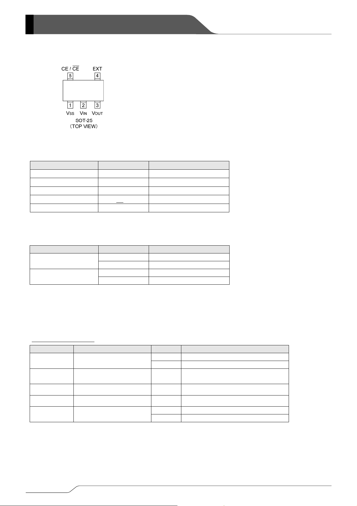
■PIN CONFIGURATION
■PIN ASSIGNMENT
PIN NUMBER PIN NAME FUNCTION
1 VSS Ground
2 VIN Supply Voltage Input
3 VOUT Regulated Voltage Output
4 EXT Base Current Control
5
■FUNCTION
SERIES CE OUTPUT VOLTAGE
XC62ER
XC62EP
H=High level
L=Low level
■PRODUCT CLASSIFICATION
●Ordering Information
XC62E①②③④⑤⑥⑦-⑧
DESIGNATOR DESCRIPTION SYMBOL DESCRIPTION
①
②③
④
(*1)
CE Pin Logic
Output Voltage 15 ~ 60
Temperature Characteristics 0
CE/CE
H ON
L OFF
H OFF
L ON
Chip Enable
R Positive
P Negative
e.g. VOUT 1.5Vt②=1, ③=5
VOUT 6.0Vt②=6, ③=0
±100ppm (TYP.)
⑤
⑥⑦-⑧
(*1)
The “-G” suffix indicates that the products are Halogen and Antimony free as well as being fully RoHS compliant.
(*2)
The device orientation is fixed in its embossed tape pocket. For reverse orientation, please contact your local Torex sales office or
representative. (Standard orientation: ⑥R-⑧, Reverse orientation: ⑥L-⑧)
Output Voltage Accuracy 2
Packages
Taping Type
(*2)
MR SOT-25
MR-G SOT-25
±2%
2/12
A
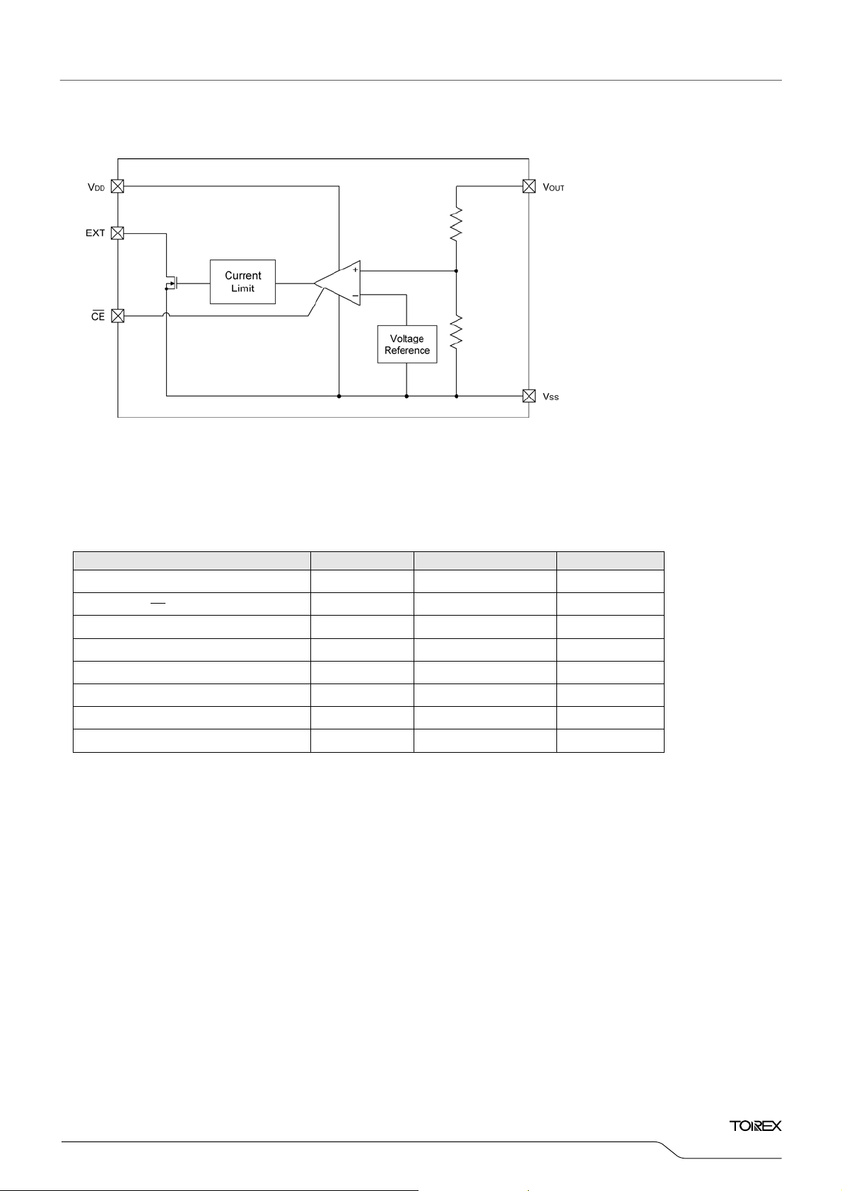
■BLOCK DIAGRAM
■
BSOLUTE MAXIMUM RATINGS
PARAMETER SYMBOL RATINGS UNITS
VIN Input Voltage VIN 12.0 V
VOUT Output Voltage VOUT VSS-0.3~VIN+0.3 V
CE/CE Input Voltage VCE VSS-0.3~VIN+0.3 V
EXT Output Voltage VEXT 12.0 V
EXT Output Current IEXT 50 mA
Power Dissipation Pd 150 mW
Operating Temperature Range Topr -30~+80 ℃
Storage Temperature Range Tstg -40~+125 ℃
Ta = 25℃
XC62E
Series
3/12
XC62E Series
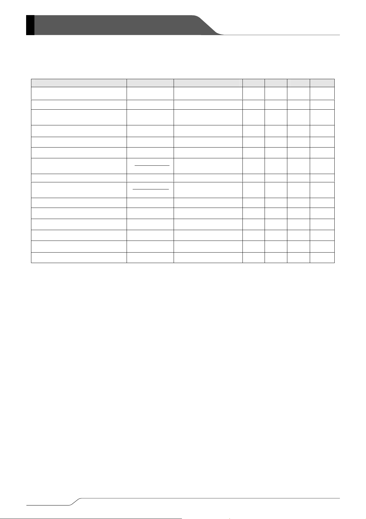
■ELECTRICAL CHARACTERISTICS
XC62EP3002
Maximum Output Current* IOUT max VIN=4.0V - 1000 - mA
VOUT(T)=3.0V
PARAMETER SYMBOL CONDITIONS MIN. TYP. MAX. UNITS
Output Voltage
Load Regulation
(*6)
Dropout Voltage (*3) Vdif
(*1)
OUT(E)
△V
OUT
(*2)
V
Ta=25℃
OUT=50mA
I
V
IN=4.0V
V
IN=4.0V
1mA≦IOUT≦100mA
OUT=100mA - 100 - mV
I
2.940 3.000 3.060 V
-60 - 60 mV
Supply Current 1 ISS1 VIN=4.0V, VCE=VSS - 50 80
Supply Current 2 ISS2 VIN=8.0V,VCE=VIN - - 0.6
Line Regulation
(*6)
Input Voltage
Output Voltage
Temperature Characteristics
(*6)
△V
OUT
△V
IN・VOUT
IN
△V
△V
OUT
△Topr・V
OUT
IOUT=50mA
4.0V≦VIN≦8.0V
- - 8.0 V
IOUT=10mA
-30℃≦Topr≦80℃
- 0.1 0.3 %V
-
±100
-
EXT Output Voltage VEXT - - 8.0 V
EXT Leak Current ILEAK - - 0.5
CE "High" Level Voltage VCEH 1.5 - - V
CE "Low" Level Voltage VCEL - - 0.25 V
CE "High" Level Current ICEH VCE=VIN - - 0.1
CE "Low" Level Current ICEL VCE=VSS -0.2 -0.05 0
The characteristics for the XC62ER series are the same as above except for the CE operating logic, which is the opposite.
NOTE:
OUT(T)=Specified output voltage.
*1: V
*3: Vdif= {V
*4: V
*5: V
*6: The characteristics for the parameters are liable to vary depending on which transistor is used.
*7: The maximum output current value is not a value representing continuous output due to the limitations of the 2AS1213
OUT(E)=Effective output voltage (i.e. the output voltage when "VOUT(T)+1.0V" is provided at the VIN pin while maintaining
*2: V
a certain I
Please use a transistor with a low saturation voltage level and hFE equal to 100 or more.
transistor's power dissipation.
OUT value).
(*5)
IN1
OUT1= A voltage equal to 98% of the output voltage whenever an amply stabilized IOUT {VOUT(T)+1.0V} is input.
IN1=The input voltage when VOUT1 appears as input voltage is gradually decreased.
-VOUT1
(*4)
}
μA
μA
ppm/℃
μA
μA
μA
4/12

■ELECTRICAL CHARACTERISTICS (Continued)
XC62EP4002
VOUT(T)=4.0V(*1)
Ta=25℃
PARAMETER SYMBOL CONDITIONS MIN. TYP. MAX. UNITS
I
Output Voltage VOUT(E)
(*2)
OUT=50mA
V
IN=5.0V
3.920 4.000 4.080 V
Maximum Output Current (*6) IOUT max VIN=5.0V - 1000 - mA
V
Load Regulation
(*6)
△VOUT
1mA≦I
IN=5.0V
OUT≦100mA
-60 - 60 mV
Dropout Voltage (*3) Vdif IOUT=100mA - 100 - mV
Supply Current 1 ISS1 VIN=5.0V, VCE=VSS - 50 80 μA
Supply Current 2 ISS2 VIN=8.0V,VCE=VIN - - 0.6 μA
Line Regulation
(*6)
△V
OUT
IN・VOUT
IOUT=50mA
5.0V≦V
IN≦8.0V
- 0.1 0.3 %V
△V
Input Voltage VIN - - 8.0 V
Output Voltage
Temperature Characteristics
(*6)
OUT
△V
△Topr・V
OUT
IOUT=10mA
-30℃≦Topr≦80℃
- ±100 - ppm/℃
EXT Output Voltage VEXT - - 8.0 V
EXT Leak Current ILEAK - - 0.5 μA
CE "High" Level Voltage VCEH 1.5 - - V
CE "Low" Level Voltage VCEL - - 0.25 V
CE "High" Level Current ICEH VCE=VIN - - 0.1 μA
CE "Low" Level Current ICEL VCE=VSS -0.2 -0.05 0 μA
XC62EP4002
OUT(T)=5.0V(*1)
V
Ta=25℃
PARAMETER SYMBOL CONDITIONS MIN. TYP. MAX. UNITS
I
Output Voltage VOUT(E)
(*2)
OUT=50mA
V
IN=6.0V
4.940 5.000 5.100 V
Maximum Output Current (*6) IOUT max VIN=6.0V - 1000 - mA
Load Regulation (*6) △VOUT
1mA≦I
IN=6.0V
OUT≦100mA
-60 - 60 mV
V
Dropout Voltage (*3) Vdif IOUT=100mA - 100 - mV
Supply Current 1 ISS1 VIN=6.0V, VCE=VSS - 50 80 μA
Supply Current 2 ISS2 VIN=8.0V,VCE=VIN - - 0.6 μA
Line Regulation (*6)
△V
OUT
IN・VOUT
IOUT=50mA
6.0V≦V
IN≦8.0V
- 0.1 0.3 %V
△V
Input Voltage VIN - - 8.0 V
Output Voltage
Temperature Characteristics (*6)
OUT
△V
△Topr・V
OUT
IOUT=10mA
-30℃≦Topr≦80℃
- ±100 - ppm/℃
EXT Output Voltage VEXT - - 8.0 V
EXT Leak Current ILEAK - - 0.5 μA
CE "High" Level Voltage VCEH 1.5 - - V
CE "Low" Level Voltage VCEL - - 0.25 V
CE "High" Level Current ICEH VCE=VIN - - 0.1 μA
CE "Low" Level Current ICEL VCE=VSS -0.2 -0.05 0 μA
The characteristics for the XC62ER series are the same as above except for the CE operating logic, which is the opposite.
Note: *1. V
*2. V
*3. Vdif= {V
*4. V
*5. V
*6. The characteristics for the parameters are liable to vary depending on which transistor is used.
*7. The maximum output current value is not a value representing continuous output due to the limitations of the 2AS1213
OUT(T)=Specified output voltage.
OUT(E)=Effective output voltage (i.e. the output voltage when "VOUT(T)+1.0V" is provided at the VIN pin while maintaining a
OUT value).
certain I
OUT1= A voltage equal to 98% of the output voltage whenever an amply stabilized IOUT {VOUT(T)+1.0V} is input.
IN1= The input voltage when VOUT1 appears as input voltage is gradually decreased.
Please use a transistor with a low saturation voltage level and hFE equal to 100 or more.
transistor's power dissipation.
IN1
(*5)
-VOUT1
(*4)
}
XC62E
Series
5/12

V
XC62E Series
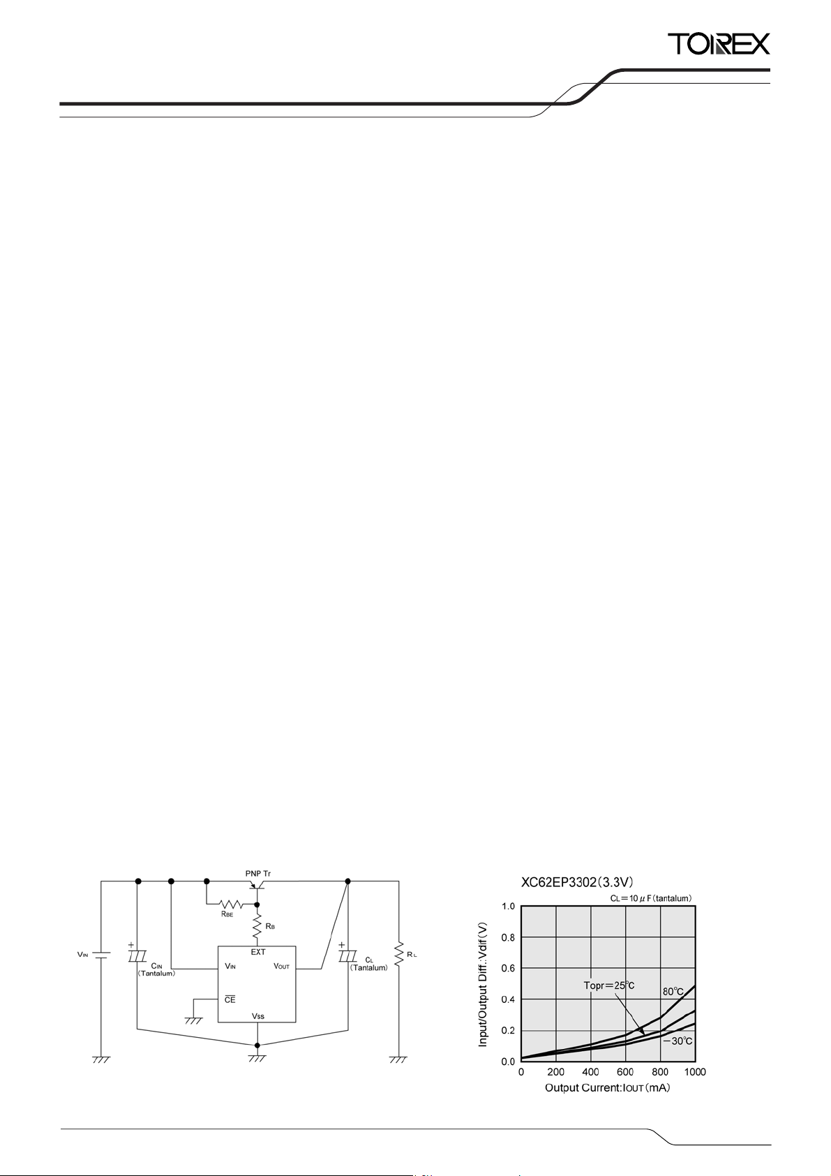
■TYPICAL APPLICATION CIRCUIT
●Standa rd Circuit
IN
■OPERATIONAL EXPLANATION
Output voltage (VOUT) can be fixed by revising the external transistor's base current. This can be done by comparing the
detected voltage level and the setting voltage power supply level.
With the XC62EP (CE negative voltage), if a voltage above the CE pin's "H" level is applied, the IC will enter stand-by mode
where the base and differential amplifier's currents are regulated.
C
IN
(Tantalum)
PNP Tr
R
BE
R
B
EXT
V
IN
CE
Vss
V
OUT
L
C
(Tantalum)
External Components:
L
R
PNP Tr.: 2SA1213
RBE: 20kΩ ~ 47kΩ
RB: Please refer to Note 2 on the following page.
C
IN: 10μF (Tantalum)
CL: 47μF (Tantalum) 10μF minimum
■NOTES ON USE
1. PNP Transistor
The selection of a transistor should take into account output current, input voltage and power dissipation for each specific
application. It is recommended that a transistor that has a low output saturated voltage (V
characteristics be used.
2. RB Resistor
Although the IC unit is protected by a base current remitter circuit, it is recommended that a resistor (R
between the transistor's base and the IC's EXT pin to protect the transistor.
Required output current can be calculated using the follo wing equation althou gh characteristic variation s and conditions
of use should be carefully checked before use. The following equation also indicates the conditions needed to obtain I
(MAX.) at V
3. RBE Resistor, CL Capacitor
To prevent oscillation due to output load variation, use of a phase compensation c apacitor CL is recommended. Please
use a Tantalum capacitor of at least 10mF. Please also use an RBE resistor of less than 47kΩ.
An RBE resistor of between 20kΩ and 47kΩ is recommended for less power consumption.
4. Input Impedance
In order to control oscillation brought about as a result of impedance at the power supply line, connect a capacitor of
10μF or more (Tantalum) between the external transistor's emitter and the ground pin.
●Protection Circuit
IN (MIN.). However, the larger the input current, the larger the output current (IOUT) that can be obtained.
VIN (MIN.)-1.2(V)
B
R
0.7(V)
RBE
IOUT (MAX.)
hFE
The built-in protection circuit is to protect the IC only. Therefore to prevent output shorts and overshoot current through
the transistor, use of a resistor RB or an overshoot current protection circuit is recommended.
Care should also be taken with the transistor's power dissipation.
CE) and high hFE
B) be connected
OUT
6/12

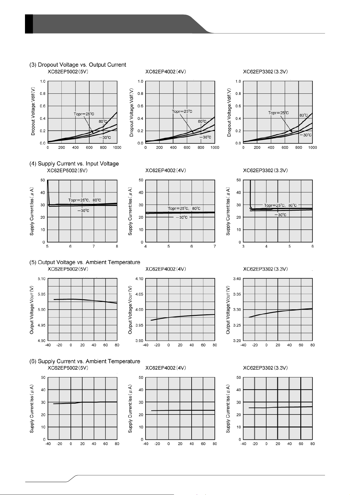
■TYPICAL PERFORMANCE CHARACTERISTICS
XC62E
Series
7/12
)
)
)
)
)
)
XC62E Series
■TYPICAL PERFORMANCE CHARACTERISTICS (Continued)
CL=10μF (tantalum
Output Current: IOUT (mA)
Input Voltage: VIN (V)
Input Voltage: VIN (V) Input Voltage: VIN (V)
IOUT=100mA, CL=10μF (tantalum
VIN=6V
IOUT=100mA, CL=10μF (tantalum
VIN=6V VIN=5V VIN=4.3V
Ambient Temperature: Topr (℃) Ambient Temperature: T opr (℃) Ambient Temperature: Topr (℃)
CL=10μF (tantalum
Output Current: IOUT (mA)
VIN=5V
IOUT=100mA, CL=10μF (tantalum
Ambient Temperature: Topr (℃) Ambient Temperature: Topr (℃) Ambient Temperature: Topr (℃)
CL=10μF (tantalum
VIN=4.3V
8/12

■TYPICAL PERFORMANCE CHARACTERISTICS (Continued)
(7) Input Transient Respon se
XC62E
Series
9/12
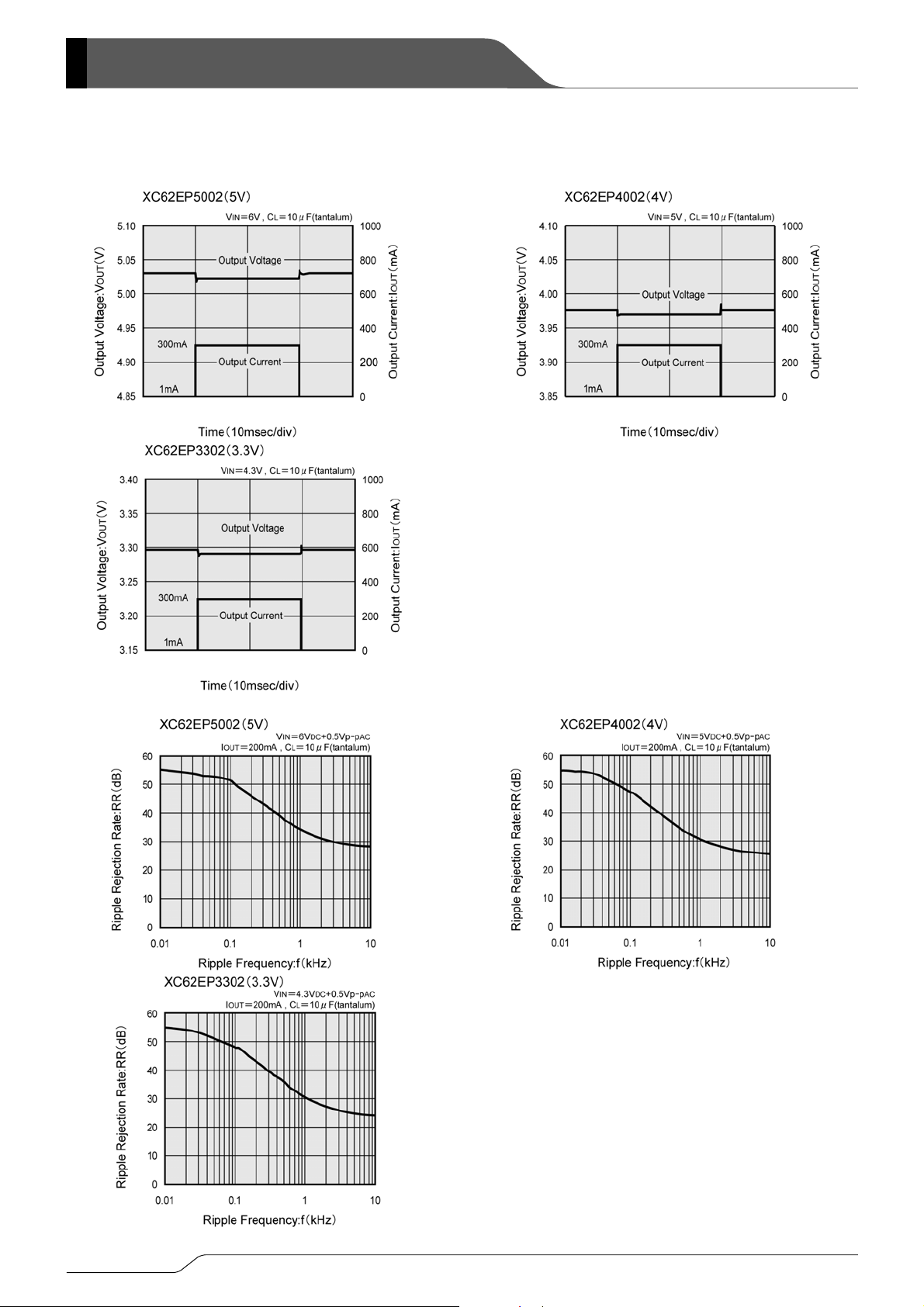
XC62E Series
■TYPICAL PERFORMANCE CHARACTERISTICS (Continued)
(8) Load Transient Response
(9) Ripple Rejection Rate
10/12
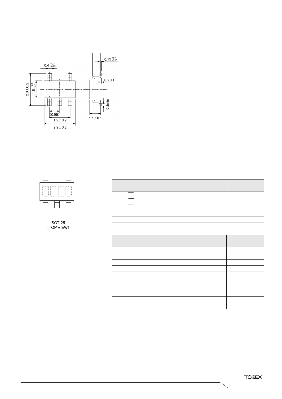
■PACKAGING INFORMATION
●SOT-25
■MARKING RULE
●SOT-25
54
① ② ③ ④
123
① not used
② represents integer of output voltage
③ represents decimal number of output voltage
MARK
(XC62ER Type)
VOLTAGE (V)
2 2.x 2 2.x
3 3.x 3 3.x
4 4.x 4 4.x
5 5.x 5 5.x
6 6.x 6 6.x
MARK
(XC62ER Type)
VOLTAGE (V)
0 x.0 0 x.0
1 x.1 1 x.1
2 x.2 2 x.2
3 x.3 3 x.3
4 x.4 4 x.4
5 x.5 5 x.5
6 x.6 6 x.6
7 x.7 7 x.7
8 x.8 8 x.8
9 x.9 9 x.9
④ based on internal standards
MARK
(XC62EP Type)
MARK
(XC62EP Type)
XC62E
Series
VOLTAGE (V)
VOLTAGE (V)
11/12

XC62E Series
1. The product s and product specification s contained he rein are subject to change without
notice to improve performance characteristics. Consult us, or our representatives
before use, to confirm that the information in this datasheet is up to date.
2. We assume no responsibility for any infringement of patents, patent rights, or other
rights arising from the use of any information and circuitry in this datasheet.
3. Please ensure suitable shipping controls (including fail-safe designs and aging
protection) are in force for equipment employing products listed in this datasheet.
4. The products in this datasheet are not developed, designed, or approved for use with
such equipment whose failure of malfunction can be reasonably expected to directly
endanger the life of, or cause significant injury to, the user.
(e.g. Atomic energy; aerospace; transport; combustion and associated safety
equipment thereof.)
5. Please use the products listed in this datasheet within the specified ranges.
Should you wish to use the products under conditions exceeding the specifications,
please consult us or our representatives.
6. We assume no responsibility for damage or loss due to abnormal use.
7. All rights reserved. No part of this datasheet may be copied or reproduced without the
prior permission of TOREX SEMICONDUCTOR LTD.
12/12
 Loading...