

XC6225 Series
30mA High Speed LDO Regulator
■GENERAL DESCRIPTION
The XC6225 series is a high accuracy, low noise, and low dropout CMOS LDO regulator. The series includes a
reference voltage source, an error amplifier, a driver transistor, a current limiter, and a phase compensation circuit.
The CE function enables the entire circuit to be turned off by a low level input signal to the CE pin. In this stand-by
state, the XC6225B series can discharge the electric charge stored at the output capacitor through the internal
auto-discharge switch, and as a result the V
(CL) is also compatible with low ESR ceramic capacitors. Output voltage is selectable in 0.05V increments within a
range of 0.8V~5.0V. The current limit fold-back circuit works as a short circuit protection as well as the output current
limiter. The series achieves a fast response with only 25μA of low power consumption. The current limit is set to
50mA (TYP.) so that the device is optimized to protect the circuit from over-current. It is ideally suited for applications
requiring 30 mA or less.
A small USP-4 package makes high density mounting possible.
■APPLICATIONS
● Cellular phones
● Cordless phones,
Wireless communication equipment
● Portable games
● Cameras, VCRs
● Portable AV equipment
● PDAs
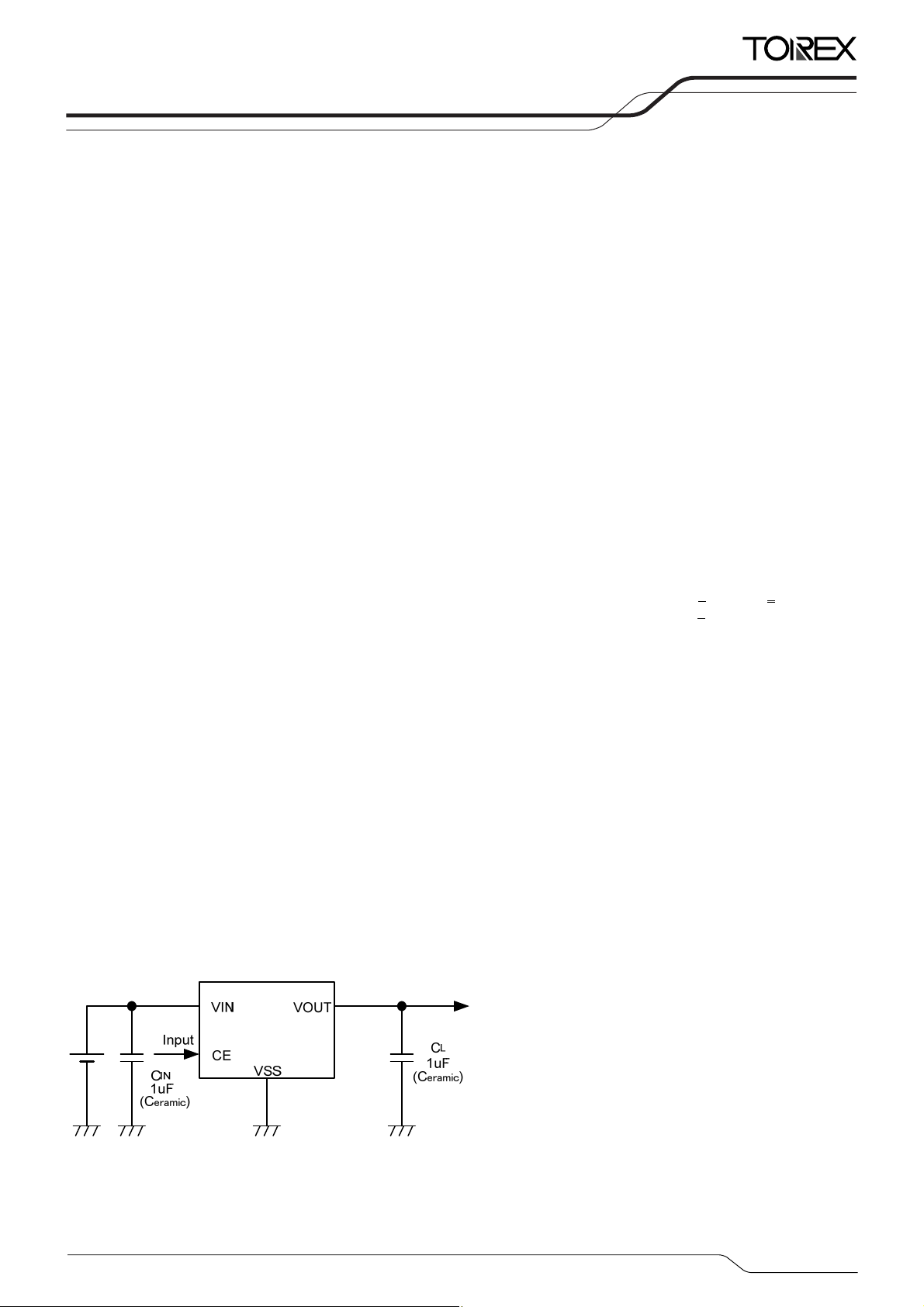
■TYPICAL APPLICATION CIRCUIT
OUT pin quickly returns to the VSS level. The output stabilization capacitor
■FEATURES
Output Current : 30mA <50mA (TYP.) Limit>
Dropout Voltage : 70mV@ IOUT=30mA, VOUT=3.2V
Operating Voltage Range : 2.5V ~ 6.0V
: 0.8V~5.0V (0.05V increments) Output Voltage Range
Accuracy
Low Power Consumption
Stand-by Current
High Ripple Rejection : 70dB @ 1kHz
Operating Temperature
Range
Output Capacitor : 1.0μF ceramic capacitor
CL High-Speed Auto-Discharge (XC6225B)
Low Output Noise
Packages : USP-4, SOT-25
Environmentally Friendly
2% (VOUT>1.5V)
: +
0.03V (VOUT≦1.45V)
+
: 25μA (TYP.)
: Less than 0.1μA
: -40℃~+85℃
SSOT-24
: EU RoHS Compliant, Pb Free
(under development)
ETR0342-003
1/15
XC6225 Series
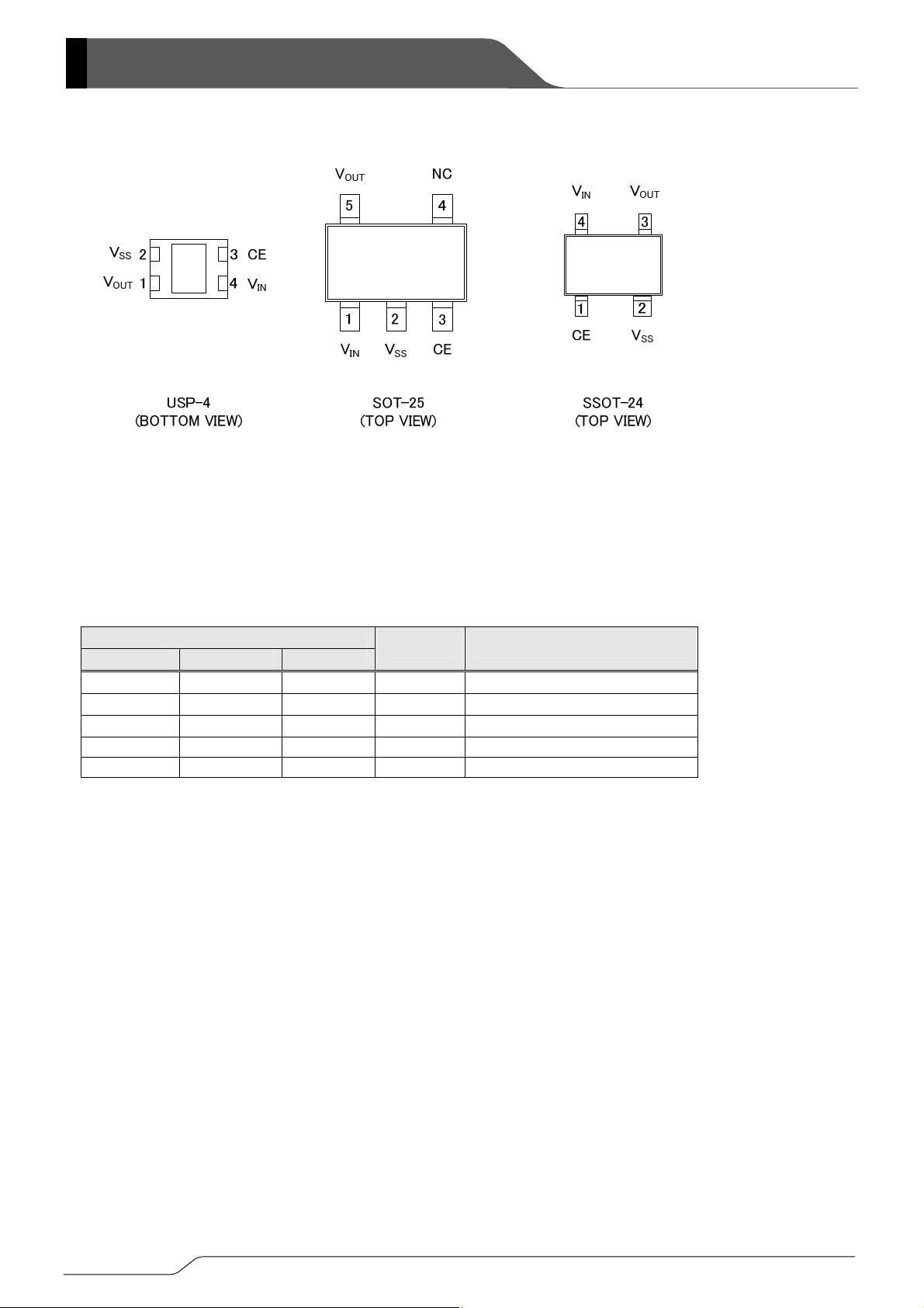
■PIN CONFIGURATION
*The heat sink pad of the USP-4 is recommended
to be soldered to enhance the strength. Please
refer to the reference mount pattern and metal
mask pattern. This pad should be electrically
opened or connected to the V
SS (No.2) pin.
(under development)
■PIN ASSIGNMENT
PIN NUMBER
USP-4 SOT-25 SSOT-24
4 1 4 VIN
1 5 3 V
2 2 2 VSS
3 3 1 CE ON/OFF Control
- 4 - NC No Connection
*SSOT-24 is under development.
PIN NAME FUNCTIONS
Power Input
OUT
Output
Ground
2/15
■PRODUCT CLASSIFICATION
●Ordering Information
XC6225①②③④⑤⑥-⑦
DESIGNATOR DESCRIPTION SYMBOL DESCRIPTION
①
② ③
④
Type of Regulator
(*1)
Output Voltage
Output Voltage
Accuracy
A CE High Active, Without CL discharge function
B CE High Active, With CL discharge function
08~50 e.g. 3.0V → ①=3, ②=0
nd
2
A
Output voltage is { x.x0V } (the 2
2% (V
≧1.5V), Within ±0.03V (V
OUT(T)
Output voltage is { x.x5V } (the 2
±2% (V
≧1.55V), Within ±0.03V (V
OUT
decimal place is “0”)
OUT(T)
nd
decimal place is “5”)
OUT
XC6225
Series
≦1.40V)
≦1.45V)
⑤⑥-⑦
(*1)
The ”-G” suffix indicates that the products are Halogen and Antimony free as well as being fully RoHS compliant.
(*2)
The device orientation is fixed in its embossed tape pocket.
For reverse orientation, please contact your local Torex sales office or representative.
(Standard orientation: ⑤R-⑦, Reverse orientation: ⑤L-⑦)
Packages
Taping Type
(*2)
GR-G USP-4
MR-G SOT-25
NR-G
SSOT-24(under development)
3/15
XC6225 Series
■BLOCK DIAGRAMS
*Diodes inside the circuit are an ESD protection diode and a parasitic diode.
●XC6225A Series
●XC6225B Series
■ABSOLUTE MAXIMUM RATINGS
PAR AMET ER SYMBOL RATINGS UNITS
Input Voltage VIN V
Output Current I
Output Voltage V
CE Input Voltage VCE VSS-0.3~+6.5 V
Power Dissipation
Operating Temperature Range Topr -40~+85 ℃
Storage Temperature Range Tstg -55~+125 ℃
(*1)
I
≦ Pd / (VIN-V
OUT
*SSOT-24 is under development.
OUT
)
USP-4 120
SOT-25 250
SSOT-24
OUT
OUT
Pd
-0.3~+6.5 V
SS
400
V
SS
(*1)
mA
-0.3~VIN+0.3 V
150
Ta=25℃
mW
4/15
XC6225
Series
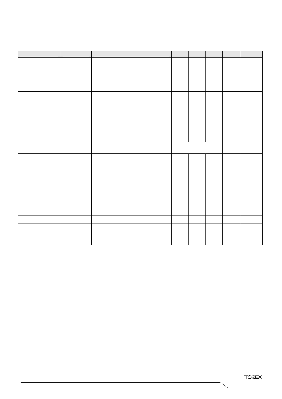
■ELECTRICAL CHARACTERISTICS
●XC6225A/B Series Ta=25℃
PAR AMET ER SYMBOL CONDITIONS
V
≧1.50V
OUT(T)
Output Voltage
V
OUT(E)
(*2)
V
V
V
CE=VIN
OUT(T)
CE=VIN
, I
=10mA
OUT
≦1.45V
, I
=10mA
OUT
VCE=VIN
V
IN
Output Current I
OUTMAX
1.5V≦V
V
CE=VIN
V
IN
0.8V≦V
V
Load Regulation ΔV
Dropout Voltage
(*5)
Vdif I
OUT
Supply Current ISS V
CE=VIN
0.1mA≦I
OUT
IN=VOUT
= V
=2.5V
=30mA, VCE=VIN
OUT(T)
OUT(T)
OUT(T)
+1.0V, I
+1.0V
≦30mA
OUT
≦5.0V
≦1.45V
=0mA - 25 50 μA ②
OUT
MIN. TYP. MAX.
(*4)
×1.02
+0.03
×0.98
(*3)
-0.03
(*3)
V
OUT(T)
30 50 - mA ①
- 5 12 mV ①
DROPOUT VOLTAGE
CHART
UNITS CIRCUIT
(*3)
(*3)
mV ①
V ①
Stand-by Current
Line Regulation
(ΔV
V
I
STBY
ΔV
/
OUT
IN・VOUT
=6.0V, VCE=VSS - 0.01 0.1 μA ②
IN
V
+0.5V≦VIN≦6.0V
OUT(T)
V
≧2.0V,
OUT(T)
V
)
2.5V≦VIN≦6.0V
V
V
CE=VIN
OUT(T)
CE=VIN
, I
=10mA
OUT
≦1.95V
, I
=10mA
OUT
- 0.01 0.20 %/V ①
Input Voltage VIN 2.5 - 6.0 V ①
Output Voltage
Temperature
Characteristics
ΔV
OUT
(ΔTa ・V
/
OUT
V
CE=VIN
-40℃≦Ta ≦85℃
)
, I
OUT
=30mA
- ±100 -
ppm/
℃
①
5/15

XC6225 Series
■ELECTRICAL CHARACTERISTICS (Continued)
●XC6225A/B Series (Continued)
PAR AMET ER SYMBOL CONDITIONS
VIN=5.75VDC+0.5Vp-pAC
Ripple Rejection
Rate
Limit Current1
Limit Current2
Limit Current3
(*9)
I
(*9, *10)
(*9, *10)
Short Current
CE High Level
Voltage
CE Low Level Voltage
CE High Level
Current
I
I
5.0V≧V
V
CE=VIN
VIN={V
4.75V≧V
V
PSRR
CE=VIN
VIN={V
4.0V≧V
V
CE=VIN
VIN=2.75VDC+0.5Vp-pAC
1.7V≧V
V
CE=VIN
V
=6.0V, VCE=V
LIM1
LIM 2
IN
5.0V≧V
VIN=V
OUT(T)
5.0V≧V
VIN=2.5V
1.45V≧V
VIN=V
OUT(T)
5.0V≧V
LIM 3
VIN=2.5V
2.35V≧V
V
I
SHORT
V
CEH
V
- - 0.3 V
CEL
I
VCE=VIN -0.1 - 0.1 μA ④
CEH
CE=VIN
V
OUT is short-circuited at the VSS level
≧4.8V
OUT(T)
, I
=30mA, f=1kHz
OUT
+1.0}VDC+0.5Vp-pAC
OUT(T)
≧4.05V
OUT(T)
, I
=30mA, f=1kHz
OUT
+1.0}VDC+0.5Vp-pAC
OUT(T)
≧1.75V
OUT(T)
, I
=30mA, f=1kHz
OUT
≧0.8V
OUT(T)
, I
=30mA, f=1kHz
OUT
IN
≧0.8V
OUT(T)
+1.0V, VCE=V
≧1.5V
OUT(T)
≧0.8V
OUT(T)
+0.1V
≧2.4V
OUT(T)
≧1.55V
OUT(T)
IN
Ta =2 5℃
MIN. TYP. MAX.
UNITS CIRCUIT
- 60 -
dB ③
- 70 -
30 50 70
30 50 70
mA ①
- 50 70
- 15 - mA ①
1.2 - 6.0 V ④
④
CE Low Level Current
CL Auto-Discharge
Resistance
NOTE:
* 1: Unless otherwise stated regarding input voltage conditions, 1.5V≦V
* 2: V
OUT (E) = Effective output voltage (Refer to the voltage chart)
(I.e. the output voltage when stabilized "V
* 3: The output voltage V
* 4: V
OUT (T) = Nominal output voltage
* 5: Vdif ={V
* 6: V
OUT1=A voltage equal to 98% of the output voltage when an amply stabilized {VOUT (T) +1.0V} is input.
* 7: V
IN1= The input voltage when VOUT1 appears at the V
* 8: For the XC6225B series only. The XC6225A series discharges by using the two resistors R1 and R2 shown in the block diagram.
*9: Limit current is defined as the output current when V
*10: The device may not satisfy the specification values when it is used with the input voltages lower than the conditions of I
IN1
(*8)
(*7)
-VOUT1
I
VCE=VSS -0.1 - 0.1 μA ④
CEL
R
VIN=6.0V, V
DCHG
OUT (E) is shown in the voltage chart.
(*6)
}
OUT
OUT (T) +1.0V" is provided at the VIN pin while maintaining a certain IOUT value.)
OUT
OUT(E)
=4.0V, VCE= VSS - 780 - Ω ①
≦5.0V is VIN=V
OUT(T)
pin while input voltage is gradually decreased.
x 0.95 is impressed at the V
+1.0V, and 0.8V≦V
OUT(T)
pin.
OUT
≦1.45V is VIN=2.5V.
OUT(T)
(1.45V≧V
LIM2
≧0.8V) and I
OUT(T)
LIM3
.
6/15

■OUTPUT VOLTAGE CHART
●Voltage Table1
NOMINAL
OUTPUT
VOLTAGE
(V)
V
OUT(T)
OUTPUT VOLTAGE
±2% (V)
V
Vdif
OUT(E)
MIN. MAX. TYP. MAX.
0.80 0.7700 0.8300 1700
0.85 0.8200 0.8800
0.90 0.8700 0.9300 1600
0.95 0.9200 0.9800
1.00 0.9700 1.0300 1500
1.05 1.0200 1.0800
1.10 1.0700 1.1300 1400
1.15 1.1200 1.1800
DROPOUT VOLTAGE
Vdif
(mV)
325
235
160
115
1650
1550
1450
1350
1.20 1.1700 1.2300 1300
1.25 1.2200 1.2800 1250
1.30 1.2700 1.3300 1200
1.35 1.3200 1.3800 1150
85
1.40 1.3700 1.4300 1100
1.45 1.4200 1.4800
1050
1.50 1.4700 1.5300 1000
1.55 1.5190 1.5810 950
1.60 1.5680 1.6320 900
1.65 1.6170 1.6830 850
50
1.70 1.6660 1.7340 800
1.75 1.7150 1.7850
750
1.80 1.7640 1.8360 700
1.85 1.8130 1.8870 650
1.90 1.8620 1.9380 600
1.95 1.9110 1.9890 550
2.00 1.9600 2.0400 500
2.05 2.0090 2.0910 450
2.10 2.0580 2.1420 400
2.15 2.1070 2.1930 350
40
2.20 2.1560 2.2440 300
2.25 2.2050 2.2950 250
2.30 2.2540 2.3460 200
2.35 2.3030 2.3970 150
2.40 2.3520 2.4480
2.45 2.4010 2.4990
2.50 2.4500 2.5500
2.55 2.4990 2.6010
2.60 2.5480 2.6520
2.65 2.5970 2.7030
2.70 2.6460 2.7540
2.75 2.6950 2.8050
70
120
2.80 2.7440 2.8560
2.85 2.7930 2.9070
2.90 2.8420 2.9580
2.95 2.8910 3.0090
XC6225
Series
7/15

)
XC6225 Series
■OUTPUT VOLTAGE CHART (Continued
●Voltage Table2
NOMINAL
OUTPUT
VOLTAGE
(V)
V
OUT(T)
OUTPUT VOLTAGE
±2% (V)
V
Vdif
OUT(E)
MIN. MAX. TYP. MAX.
3.00 2.9400 3.0600
3.05 2.9890 3.1110
3.10 3.0380 3.1620
3.15 3.0870 3.2130
3.20 3.1360 3.2640
3.25 3.1850 3.3150
3.30 3.2340 3.3660
3.35 3.2830 3.4170
3.40 3.3320 3.4680
3.45 3.3810 3.5190
3.50 3.4300 3.5700
3.55 3.4790 3.6210
3.60 3.5280 3.6720
3.65 3.5770 3.7230
3.70 3.6260 3.7740
3.75 3.6750 3.8250
3.80 3.7240 3.8760
3.85 3.7730 3.9270
3.90 3.8220 3.9780
3.95 3.8710 4.0290
4.00 3.9200 4.0800
4.05 3.9690 4.1310
4.10 4.0180 4.1820
4.15 4.0670 4.2330
4.20 4.1160 4.2840
4.25 4.1650 4.3350
4.30 4.2140 4.3860
4.35 4.2630 4.4370
4.40 4.3120 4.4880
4.45 4.3610 4.5390
4.50 4.4100 4.5900
4.55 4.4590 4.6410
4.60 4.5080 4.6920
4.65 4.5570 4.7430
4.70 4.6060 4.7940
4.75 4.6550 4.8450
4.80 4.7040 4.8960
4.85 4.7530 4.9470
4.90 4.8020 4.9980
4.95 4.8510 5.0490
5.00 4.9000 5.1000
8/15
DROPOUT VOLTAGE
Vdif
(mV)
70 120
95 170

XC6225
Series
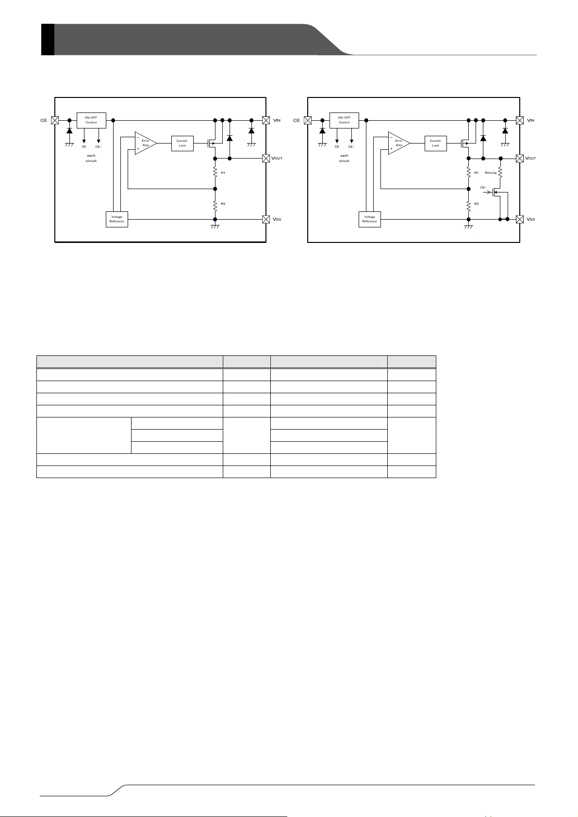
■OPERATIONAL EXPLANATION
The voltage divided by resistors R1 & R2 is compared with the internal reference voltage by the error amplifier. The P-channel
MOSFET connected to the V
controlled and stabilized by a system of negative feedback. The current limit circuit and short-circuit protection circuit operate in
relation to the level of output current. Further, the IC’s entire circuitry is turned off by the input signal to the CE pin.
●BLOCK DIAGRAM
CE V
ON/OFF
Control
CE CE/
each
circuit
Voltage
Reference
<Input and Output Capacitors>
The XC6225 needs an output capacitor C
the chart below. If a loss of the capacitance happens, the stable phase compensation may not be obtained. Please ensure to
use a capacitor which does not depend on bias or temperature too much. For a stable power input, please connect an input
capacitor CIN of 1.0μF between the VIN pin and the VSS pin.
OUTPUT VOLTAGE OUTPUT CAPACITOR
0.8V~1.15V CL=4.7μF
1.2V~1.35V CL=2.2μF
1.4V~4.0V CL=1.0μF
4.05V~5.0V CL=2.2μF
<C
Auto-Discharge Function>
L
XC6225B series can discharge the electric charge in the output capacitor (C
the whole IC circuit to be turned off, is inputted via the N-channel transistor located between the V
to BLOCK DIAGRAM). The C
time of the output capacitor (C
constant of the C
L auto-discharge resistance value [R
voltage after discharge via the N-channel transistor is calculated by the following formula.
V= V
OUT(E)
OUT pin, is then driven by the subsequent output signal. The output voltage at the VOUT pin is
IN
-
Error
Amp
+
auto-discharge resistance value is set at 780Ω(VOUT=4.0V @ VIN=6.0V at TYP.). The discharge
L
L) is set by the C
-t / τ
×e
or t= τln(V/ V
Current
Limit
OUT
V
R1
Rdischg
CE/
R2
SS
V
for phase compensation. Values required for the phase compensation are shown in
L
L), when a low signal to the CE pin, which enables
OUT pin and the VSS pin (refer
auto-discharge resistance (R) and the output capacitor (CL). By setting the time
L
] and the output capacitor value (CL) as τ(τ=C x R
OUT(E)
DCHG
)
DCHG
Where
V: Output voltage after discharge
V
: Output voltage
OUT (E)
t : Discharge time,
τ: C
auto-discharge resistance R
L
×Output capacitor (CL)value C
DCHG
), the output
9/15

XC6225 Series
■OPERATIONAL EXPLANATION (Continued)
<Current Limiter, Short-Circuit Protection>
The XC6225 series’ fold-back circuit operates as an output current limiter and a short protection circuit for the output pin. When
the load current reaches the current limit level, the fixed current limiter circuit operates and output voltage drops. When the output
pin is short-circuited to the V
<CE Pin>
The IC's internal circuitry can be shutdown via the signal from the CE pin with the XC6225 series. In the shutdown state, output
at the V
OUT pin will be pulled down to the VSS level via R1 & R2. However, with the XC6225B series, the CL auto-discharge
resistor is connected in parallel to R1 and R2 while the power supply is applied to the V
reaches the V
SS level is shorter.
The output voltage is in an undefined state when the CE pin is left open. If this IC is used with the correct voltage for the CE pin,
the logic is fixed and the IC will operate normally. However, the supply current may increase as a result of shoot-through current
in the IC's internal circuitry when a medium voltage is input.
■NOTES ON USE
1. Please use this IC within the stated absolute maximum ratings. The IC is liable to malfunction should the ratings be exceeded.
2. Where wiring impedance is high, operations may become unstable due to noise and/or phase lag depending on output current.
Please wire the input capacitor (C
10/15
SS pin, the current falls and reaches about 15mA.
IN pin. Therefore, time until the VOUT pin
IN) and the output capacitor (CL) as close to the IC as possible.

■TEST CIRCUITS
●Circuit①: Output Voltage, Output Current, Dropout Voltage, Line Regulation, Load Regulation, Current Limit,
Short Current, CL Discharge Resistance
●Circuit②: Supply Current, Stand-by Current
・測定回路 2(消費電流・スタンバイ電流)
●Circuit③: Ripple Rejection Rate
・測定回路 3(リップル除去率)
XC6225
Series
11/15

XC6225 Series
■TEST CIRCUITS (Continued)
●Circuit④: CE “High” “Low” Level Voltage, CE “High” “Low” Level Current
・測定回路 4(CE”H”L”レベル電圧・CE”H”L”レベル電流)
12/15

■PACKAGING INFORMATION
●USP-4 (unit: mm) ●SOT-25 (unit: mm)
●SSOT-24 (unit: mm)
(under development)
+0.2
XC6225
Series
-0.1
1.6
2.8±0.2
0.2MIN
1.3MAX
1.1±0.1
13/15

XC6225 Series
■PACKAGING INFORMATION(Continued)
●USP-4 Reference Pattern Layout ●USP-4 Reference Metal Mask Design
14/15

XC6225
Series
1. The products and product specifications contained herein are subject to change without
notice to improve performance characteristics. Consult us, or our representatives
before use, to confirm that the information in this datasheet is up to date.
2. We assume no responsibility for any infringement of patents, patent rights, or other
rights arising from the use of any information and circuitry in this datasheet.
3. Please ensure suitable shipping controls (including fail-safe designs and aging
protection) are in force for equipment employing products listed in this datasheet.
4. The products in this datasheet are not developed, designed, or approved for use with
such equipment whose failure of malfunction can be reasonably expected to directly
endanger the life of, or cause significant injury to, the user.
(e.g. Atomic energy; aerospace; transport; combustion and associated safety
equipment thereof.)
5. Please use the products listed in this datasheet within the specified ranges.
Should you wish to use the products under conditions exceeding the specifications,
please consult us or our representatives.
6. We assume no responsibility for damage or loss due to abnormal use.
7. All rights reserved. No part of this datasheet may be copied or reproduced without the
prior permission of TOREX SEMICONDUCTOR LTD.
15/15
 Loading...