


XC6224 Series
ETR0340-005
1.2V Low Voltage Operation,150mA High Speed LDO Voltage Regulator
■GENERAL DESCRIPTION
The XC6224 series is a high speed LDO regulator that features high accurate, low noise, high ripple rejection, low dropout
and low power consumption. The series consists of a voltage reference, an error amplifier, a driver transistor, a current limiter,
and a phase compensation circuit.
This IC is suitable for a local power supply placed in adjacent to the system logic LSI or others, because of low input voltage
operation, using an ultra small package USPN-4B02 (0.75mm x 0.95mm) and stable operation with a small phase
compensation capacitor (C
Also, this IC has fast transient response and high ripple rejection (70dB @ 1kHz).
The CE function enables the circuit to be in stand-by mode by inputting low level signal. In the stand-by mode, the series
enables the electric charge at the output capacitor C
quickly returns to the V
The over current protection circuit is integrated and operates when the output current reaches current limit level.
■APPLICATIONS
●Cell phones
●Digital still cameras
●Portable electronic devices
●Portable media players
●Bluetooth
●Wireless LAN
●Terrestrial digital TV tuners
■TYPICAL APPLICATION CIRCUIT
) 0.47μF.
L
SS level.
L to be discharged via the internal switch, and as a result the VOUT pin
■FEATURES
Maximum Output Current : 150mA
Operating Voltage Range : 1.2V~3.6V
High Accuracy : ±1.5% (V
: ±20mV (V
=1.25V~3.0V)
OUT
= 0.8V~1.20V)
OUT
Low Power Consumption : 33μA (TY P.)
Stand-by Current : 0.1μA
High Ripple Rejection : 70dB@1kHz
Dropout Voltage : 210mV@150mA (V
OUT
=2.8V)
Operating Temperature Range : -40℃~+85℃
Protection Circuits : Current Limiter
Short Circuit Protection
ON/OFF Control : Active High
C
Auto Discharge Function
L
Output Capacitor : Low ESR Capacitor
Packages : USPN-4B02
SSOT-24
SOT-25
Environmentally Friendly : EU RoHS Compliant, Pb Free
■TYPICAL PERFORMANCE
CHARACTERISTICS
500
450
400
[mA]
350
OUT
300
250
200
150
100
Output Current: I
50
0
XC6224x181
I
= 1 mA ⇔ 15 0mA, tr =t f=0.5 μs,
OUT
= 2.80V, Ta=25℃, CIN=CL=0.47μF
V
IN
Output Voltage
Output Current
Time [10us/div]
1.95
1.90
1.85
1.80
1.75
1.70
1.65
1.60
1.55
1.50
1.45
[V]
OUT
Output Voltage: V
1/26

XC6224 Series
■PIN CONFIGURATION
5 4
VIN
CE
14
23
VOUT
VSS
USPN-4B02
(BOTTOM VIEW)
■PIN ASSIGNMENT
PIN NUMBER
USPN-4B02 SSOT-24 SOT-25
4 4 1 VIN
1 3 5 V
4
VIN VOUT
CE
1
3
VSS
2
SSOT-24
(TOP VIEW)
VOUT
VIN
1
VSS
2
N.C.
CE
3
SOT-25
(TOP VIEW)
PIN NAME FUNCTIONS
Power Input
Output
OUT
2 2 2 VSS
3 1 3 CE
- - 4 NC
■PRODUCT CLASSIFICATION
●Ordering Information
XC6224①②③④⑤⑥-⑦
DESIGNATOR ITEM SYMBOL DESCRIPTION
①
②③
④
(*1)
CE Active High, with CL Discharge, ±1% Accuracy
Type of Regulator
Output Voltage
Output Voltage
(The 2nd Decimal Place)
A
(The Recommended Type)
B With CE pull-down
08~30 ex.) 2.5V → ②=2, ③=5
1 {x.x0V} (the 2nd decimal place is “0”)
B {x.x5V} (the 2nd decimal place is “5”)
7R-G USPN-4B02 (5,000/Reel)
Ground
ON/OFF Control
No Connection
Without CE pull-down
2/26
⑤⑥-⑦
(*1)
The “-G” suffix indicates that the products are Halogen and Antimony free as well as being fully RoHS compliant.
Packages (Order Unit)
MR-G SOT-25 (3,000/Reel)
NR-G SSOT-24 (3,000/Reel)

■BLOCK DIAGRAMS
(1) XC6224Axxxxx
XC6224
Series
(2) XC6224Bxxxxx
VIN
CE
CurrentLimit
ON/OFF
Control
each
circuit
Error
Amp
CFB
+
-
Voltage
Reference
R1
Rdischg
R2
CE
VOUT
VSS
■ABSOLUTE MAXIMUM RATINGS
PAR AMETER SYMBOL RATINGS UNITS
Input Voltage
Output Current
Output Voltage
CE Input Voltage
USPN-4B02
Power Dissipation
SSOT24
SOT-25
Operating Temperature Range
Storage Temperature Range
*1: Please use within the range of I
*2: This is a reference data taken by using the test board. Please refer to page 20~22 for details.
≦Pd/(VIN-V
OUT
VIN
CurrentLimit
CE
VIN V
180
I
OUT
V
V
OUT
VCE V
ON/OFF
Control
SS
-0.3~VIN+0.3 V
SS
SS
each
circuit
-0.3~+4.6 V
(*1)
mA
-0.3~4.6 V
Error
Amp
CFB
+
-
Voltage
Reference
R1
Rdischg
R2
CE
100
(*2)
(*2)
mW
Pd
550 (PCB mounted)
150
500 (PCB mounted)
250
600 (PCB mounted)
(*2)
Topr -40~+85 ℃
Tst g - 55~+125 ℃
)
OUT
VOUT
VSS
3/26

XC6224 Series
■ELECTRICAL CHARACTERISTICS
●XC6224Axxxxx
PAR AMET ER SYMBOL CONDITIONS MIN. TYP. MAX. UNITS
V
≧1.25V
OUT(T
V
Output Voltage
Maximum Output
Current
Load Regulation ΔV
Dropout Voltage
(*4)
OUT(E)
(*3)
I
OUTMAX
OUT
Vdif
Supply Current IDD V
Stand-by Current
Line Regulation
I
(ΔV
STBY
ΔV
OUT
IN・VOUT
V
CE=VIN, IOUT
V
OUT(T
V
CE=VIN
VCE=V
V
CE=VIN
0.1mA≦I
I
OUT
V
CE=VIN, VIN=VOUT(E)
CE=VIN, IOUT
VCE=VSS 0.01 0.4 μA ②
V
OUT(T
V
OUT(T)
/
V
CE=VIN
)
V
OUT(T
1.6V≦V
V
CE=VIN
)
=10mA
≦1.2V
)
, I
=10mA
OUT
150 - - mA ①
IN
≦150mA
OUT
=150mA
=0mA
≧1.10V
)
+0.5V≦VIN≦3.6V
, I
=10mA
OUT
≦1.05V
)
≦3.6V
IN
, I
=10mA
OUT
×0.98
(*2)
(*2)
(*3)
V
×0.985
OUT(T)
(*7)
-20mV
- 5 20 mV ①
- 33 77 μA ②
- 0.04 0.37 %/V ①
Input Voltage VIN 1.2 - 3.6 V ①
Output Voltage
Temperature
Characteristics
Ripple Rejection Rate
PSRR
Current Limit I
Short Current I
CE High Level Voltage
CE Low Level Voltage
V
V
CE High Level
Current
CE High Level
Current
CL Discharge
Resistance
V
/
ΔV
(ΔTa ・V
OUT
OUT
CE=VIN, IOUT
)
-40℃≦Ta ≦85℃
V
CE=VIN
・When 0.80V≦V
V
=3.0V+0.5Vp-pAC
IN
・2.65V≦V
V
I
OUT
VCE=VIN 150 250 - mA ①
LIM
VCE=V
SHORT
1.0 - 3.6 V ④
CEH
- - 0.3 V ④
CEL
V
I
CEH
VCE=V
I
CEL
VIN=3.6V, VCE=VSS - 450 - Ω ①
R
DCHG
CE=VIN
A Type
OUT(T
=3.3V+0.25Vp-pAC
IN
=30mA, f=1kHz
IN, VOUT
-0.1 0 0.1 μA ④
SS
(*1)
=30mA
OUT(T
≦3.00V
)
(*2)
≦2.60V,
)
- ±100 - ppm/℃ ①
- 70 - dB ③
is connected to VSS - 35 - mA ①
-0.1 0 0.1 μA ④
NOTE:
*1: Unless otherwise specified, input voltage conditions are;
0.80V≦V
2.65V≦V
2.85V≦V
*2: V
*3: V
*4: Vdif={V
*5: V
*6: V
*7: V
: Nominal output voltage
OUT(T)
: Effective output voltage
OUT(E)
This output voltages are measured at the constant current when the input voltages are stable as Note 1.
IN1
OUT1
OUT(T)
{*5}
IN1
=The input voltage when V
=A voltage equal to 98% of the output voltage whenever an amply stabilized I
±20mV is the specification value of output voltage where V
≦2.60V : {VIN=V
OUT(T)
≦2.80V : {VIN=3.3V}
OUT(T)
≦3.00V : {VIN=3.5V}
OUT(T)
{*6}
-V
OUT1
}
appears as input voltage is gradually decreased.
OUT1
OUT(T)
+1.0V}
OUT(T)
OUT
≦1.20V
{V
(*2)
OUT(T)
V
V
OUT(T)
(*2)
OUT(T)
(*2)
V
OUT(T)
+20mV
×1.015
(*7)
(*2)
V ①
E-1 mV ①
+1.0V} is input
Ta =2 5℃
CURCUITS
4/26

XC6224
■ELECTRICAL CHARACTERISTICS (Continued)
●XC6224Bxxxxx
PAR AMET ER SYMBOL CONDITIONS MIN. TYP. MAX. UNITS
V
≧1.25V
OUT(T
Output Voltage
Maximum Output
Current
V
I
Load Regulation ΔV
Dropout Voltage
(*4)
Supply Current IDD
Stand-by Current
Line Regulation
I
ΔV
(ΔV
OUT(E)
(*3)
VCE=V
OUTMAX
OUT
Vdif
VCE=VSS - 0.01 0.4 μA ②
STBY
/
OUT
)
IN・VOUT
)
, I
V
CE=VIN
OUT
V
≦1.2V, VIN=2.5V
OUT(T
)
, I
V
CE=VIN
OUT
(*1)
IN
(*1)
V
CE=VIN
0.1mA≦I
I
OUT
V
V
V
I
OUT
V
V
V
V
1.6V≦V
V
OUT
=150mA,
CE=VIN
IN=VOUT(E)
(*1)
CE=VIN
=0mA
≧1.10V
OUT(T
)
+0.5V≦VIN≦3.6V
OUT(T)
CE=VIN、IOUT
≦1.05V
OUT(T
)
≦3.6V
IN
CE=VIN、IOUT
=10mA
=10mA
150 - - mA ①
≦150mA
(*3)
×0.98
(*2)
=10mA
=10mA
(*2)
V
OUT(T)
-20mV
×0.985
(*7)
(*2)
V
(T)
OUT
V
OUT
(T)
(*2)
V
OUT(T)
(*2)
+20mV
×1.015
(*7)
(*2)
- 5 20 mV ①
E-1 mV ①
- 33 77 μA ②
- 0.04 0.37 %/V ①
Input Voltage VIN 1.2 - 3.6 V ①
Output Voltage
Temperature
Characteristics
Ripple Rejection Rate
PSRR
Current Limit I
Short Current I
CE High Level
Voltage
CE Low Level Voltage
V
CE High Level
Current
CE High Level
Current
CL Discharge
Resistance
ΔV
(ΔTa ・V
OUT
OUT
V
/
CE=VIN, IOUT
)
-40℃≦Ta ≦85℃
V
CE=VIN
・When 0.80V≦V
V
=3.0V+0.5Vp-pAC
IN
・2.65V≦V
V
I
OUT
V
LIM
VCE=V
SHORT
V
CEH
- - 0.3 V ④
CEL
I
CEH
V
I
CEL
VIN=3.6V, VCE=VSS - 450 - Ω ①
R
DCHG
CE=VIN
V
CE=VIN
B Type
CE=VSS
OUT(T
=3.3V+0.25Vp-pAC
IN
=30mA、f=1kHz
150 250 - mA ①
IN, VOUT
-0.1 0 0.1 μA ④
(*1)
=30mA
OUT(T
≦3.00V
)
(*2)
≦2.60V
)
is connected to V
- ±100 -
- 70 - dB ③
SS
- 35 - mA ①
1.0 - 3.6 V ④
- 5.5 13.0 μA ④
NOTE:
*1: Unless otherwise specified, input voltage conditions are;
0.80V≦V
2.65V≦V
2.85V≦V
*2: V
*3: V
*4: Vdif={V
*5: V
*6: V
*7: V
: Nominal output voltage
OUT(T)
: Effective output voltage
OUT(E)
This output voltages are measured at the constant current when the input voltages are stable as Note 1.
IN1
OUT1
OUT(T)
{*5}
IN1
=The input voltage when V
=A voltage equal to 98% of the output voltage whenever an amply stabilized I
±20mV is the specification value of output voltage where V
≦2.60V : {VIN=V
OUT(T)
≦2.80V : {VIN=3.3V}
OUT(T)
≦3.00V : {VIN=3.5V}
OUT(T)
{*6}
-V
OUT1
}
+1.0V}
OUT(T)
appears as input voltage is gradually decreased.
OUT1
≦1.20V.
OUT(T)
OUT
{V
OUT(T)
+1.0V} is input
Ta =2 5℃
V ①
ppm/
℃
Series
CURCUITS
①
5/26

XC6224 Series
■ELECTRICAL CHARACTERISTICS (Continued)
●Voltage Table
NOMINAL
OUTPUT
VOLTAGE (V)
V
OUT(T)
0.80 0.7800 0.8200 - -
0.85 0.8300 0.8700 - -
0.90 0.8800 0.9200 - -
0.95 0.9300 0.9700 - -
1.00 0.9800 1.0200 - -
1.05 1.0300 1.0700
1.10 1.0800 1.1200 - -
1.15 1.1300 1.1700 - -
1.20 1.1800 1.2200
1.25
1.30
1.35
1.40
1.45
1.50
1.55
1.60
1.65
1.70
1.75
1.80
1.85
1.90
1.95
2.00
2.05
2.10
2.15
2.20
2.25
2.30
2.35
2.40
2.45
2.50
2.55
2.60
2.65
2.70
2.75
2.80
2.85
2.90
2.95
3.00
OUTPUT VOLTAGE
V
OUT(E)
(V)
MIN. MAX. TYP.
1.2313 1.2687
1.2805 1.3195
1.3298 1.3702
1.3790 1.4210
1.4283 1.4717
1.4775 1.5225
1.5268 1.5732
1.5760 1.6240
1.6253 1.6747
1.6745 1.7255
1.7238 1.7762
1.7730 1.8270
1.8223 1.8777
1.8715 1.9285
1.9208 1.9792
1.9700 2.0300
2.0193 2.0807
2.0685 2.1315
2.1178 2.1822
2.1670 2.2330
2.2163 2.2837
2.2655 2.3345
2.3148 2.3852
2.3640 2.4360
2.4133 2.4867
2.4625 2.5375
2.5118 2.5882
2.5610 2.6390
2.6103 2.6897
2.6595 2.7405
2.7088 2.7912
2.7580 2.8420
2.8073 2.8927
2.8565 2.9435
2.9058 2.9942
2.9550 3.0450
(*1)
DROPOUT VOLTAGE (E-1)
(mV)
Vdif
MAX.
-
400 500
300 430
210 410
-
6/26
(*1) When V
When V
≦1.20V, the output voltage accuracy is ±20mV.
OUT(T)
≧1.25V, the output voltage accuracy is ±1.5%.
OUT(T)

p
XC6224
■ OPERATIONAL EXPLANATION
(1) XC6224Axxxxx
The voltage divided by resistors R1 & R2 is compared with the internal reference voltage by the error amplifier. The
P-channel MOSFET which is connected to the V
at the V
protection operate in relation to the level of output current. Further, the IC’s internal circuitry can be shutdown via the CE
■ NOTES ON USE
OUT pin is controlled and stabilized by a system of negative feedback. The current limit circuit and short circuit
in signal.
<Low ESR Capacitor>
The XC6224 needs an output capacitor C
to ensure the stable phase compensation, please place an output capacitor C
as possible. For a stable power input, please connect an input capacitor C
pin.
<Current Limiter, Short-Circuit Protection>
The protection circuit operates as a combination of an output current limiter and fold-back short circuit protection.
When load current reaches the current limit level, the output voltage drops. As a result, the load current starts to reduce
with showing fold-back curve. The output current finally falls at the level of 35mA when the output pin is short-circuited.
<CE Pin>
The IC's internal circuitry can be shutdown via the signal from the CE pin. In shutdown mode, output at the V
be pulled down to the V
SS level in the XC6224B series. When the CE pin is open, the output voltage becomes undefined
state in the XC6224A series because of a high active and no pull-down. Although the CE pin is equal to CMOS input
configuration, the CE pin input current which flows into a pull-down resistor will increase in the XC6224B series
1. For temporary, transitional voltage drop or voltage rising phenomenon, the IC is liable to malfunction should the ratings
be exceeded.
2. Torex places an importance on improving our products and its reliability.
However, by any possibility, we would request user fail-safe design and post-aging treatment on system or equipment.
3. Where wiring impedance is high, operations may become unstable due to the noise and/or phase lag depending on
output current. Please strengthen VIN and VSS wiring in particular.
4. The input capacitor C
IN and the output capacitor CL should be placed to the IC as close as possible with a shorter wiring.
OUT pin is then driven by the subsequent output signal. The output voltage
L and a built-in phase compensation circuit for phase compensation. In order
(2) XC6224Bxxxxx
of 0.47μF or bigger at the V
L
IN of 0.47μF between the VIN pin and the VSS
pin as close
OUT
OUT pin will
Series
7/26

XC6224 Series
■TEST CIRCUITS
●Circuit ①
VIN
CIN:0.47μF
(ceramic)
V
CE
VSS
VOUT
CL:0.47μF
(ceramic)
A
IOUT
V
●Circuit ②
●Circuit ③
8/26
●Circuit ④
CIN:0.47μF
(ceramic)
VIN
CE
A
V
VSS
VOUT
CL:0.47μF
(ceramic)
V

V
■TYPICAL PERFORMANCE CHARACTERISTICS
(1) Output Voltage vs. Output Current
XC6224
Series
XC6224x121
1.4
VIN=2.2V CIN=CL=0.47μF
1.2
[V]
1.0
OUT
0.8
0.6
0.4
Output Voltage: V
0.2
0.0
0 50 100 150 200 250 300 350 400 450 500
Output Current: I
XC6224x181
2.1
[mA]
OUT
VIN=2.8V CIN=CL=0.47μ
1.8
[V]
1.5
OUT
1.2
0.9
0.6
Output Voltage: V
0.3
0.0
0 50 100 150 200 250 300 350 400 450 500
Output Current: I
OUT
[mA]
-40℃
25℃
85℃
-40℃
25℃
85℃
XC6224x121
1.4
1.2
[V]
1.0
OUT
0.8
Ta=25℃ CIN=CL=0.47μF
VIN=1.3V
VIN=1.7V
VIN=2.2V
VIN=3.6V
0.6
0.4
Output Voltage: V
0.2
0.0
0 50 100 150 200 250 300 350 400 450 500
Output Current: I
OUT
[mA]
XC6224x181
2.1
Ta=25℃ CIN=CL=0.47μF
1.8
[V]
1.5
OUT
1.2
0.9
0.6
Output Voltage: V
0.3
0.0
0 50 100 150 200 250 300 350 400 450 500
Output Current: I
OUT
[mA]
VIN=1.9V
VIN=2.3V
VIN=2.8V
VIN=3.6
XC6224x251
3.0
2.5
[V]
OUT
2.0
VIN=3.5V CIN=CL=0.47μF
1.5
1.0
Output Voltage: V
0.5
0.0
0 50 100 150 200 250 300 350 400 450 500
Output Current: I
OUT
[mA]
-40℃
25℃
85℃
XC6224x251
3.0
2.5
[V]
OUT
2.0
Ta=25℃ CIN=CL=0.47μF
1.5
1.0
Output Voltage: V
0.5
0.0
0 50 100 150 200 250 300 350 400 450 500
Output Current: I
OUT
[mA]
VIN=2.6V
VIN=3.0V
VIN=3.5V
VIN=3.6V
9/26
A
XC6224 Series
■TYPICAL PERFORMANCE CHARACTERISTICS (Continued)
(2) Output Voltage vs. Input Voltage
XC6224x121
I
=30mA CIN=CL=0.47μF
1.4
OUT
1.2
[V]
1.0
OUT
0.8
0.6
0.4
Output Voltage: V
0.2
-40℃
25℃
85℃
0.0
0.0 0.4 0.8 1.2 1.6 2.0 2.4 2.8 3.2 3.6
Input Voltage: V
[V]
IN
XC6224x181
I
=30mA CIN=CL=0.47μF
2.1
OUT
1.8
[V]
1.5
OUT
1.2
0.9
0.6
Output Voltage: V
0.3
0.0
0.0 0.4 0.8 1.2 1.6 2.0 2.4 2.8 3.2 3.6
Input Voltage: V
[V]
IN
-40℃
25℃
85℃
XC6224x121
1.4
Ta=25℃ CIN=CL=0.47μF
1.2
[V]
1.0
OUT
0.8
0.6
IOUT=1mA
0.4
Output Voltage: V
0.2
IOUT=30mA
IOUT=100mA
0.0
0.0 0.4 0.8 1.2 1.6 2.0 2.4 2.8 3.2 3.6
Input Voltage: V
[V]
IN
XC6224x181
Ta=25℃ CIN=CL=0.47μF
2.1
1.8
[V]
1.5
OUT
1.2
0.9
0.6
Output Volt age: V
0.3
IOUT=1 mA
IOUT=30mA
IOUT=100m
0.0
0.0 0.4 0.8 1.2 1.6 2.0 2.4 2.8 3.2 3.6
Input Voltage: V
[V]
IN
10/26
XC6224x251
I
=30mA CIN=CL=0.47μF
3.0
OUT
2.5
[V]
OUT
2.0
1.5
1.0
Output Voltage: V
0.5
-40℃
25℃
85℃
0.0
0.0 0.4 0.8 1.2 1.6 2.0 2.4 2.8 3.2 3.6
Input Voltage: V
[V]
IN
XC6224x251
3.0
Ta=25℃ CIN=CL=0.47μF
2.5
[V]
OUT
2.0
1.5
1.0
Output Voltage : V
0.5
IOUT=1mA
IOUT=30mA
IOUT=100mA
0.0
0.00.4 0.81.21.62.02.42.8 3.23.6
Input Voltage: V
[V}
IN
■TYPICAL PERFORMANCE CHARACTERISTICS (Continued)
(3) Dropout Voltage vs. Output Current
XC6224
Series
XC6224x121
1000
800
600
400
200
Dro pout Vo ltage: Vdif[V]
0
0 25 50 75 100 125 150
300
250
200
150
-40℃
25℃
85℃
Output Current: I
XC6224x251
-40℃
25℃
85℃
OUT
[mA]
CIN=CL=0.47μF
CIN=CL=0.47μF
XC6224x181
500
-40℃
400
300
200
100
Dropout Voltage: Vdif[V]
0
0 25 50 75 100 125 150
25℃
85℃
Output Current: I
OUT
CIN=CL=0.47μF
[mA]
100
Dropout Voltage: Vdif[V]
50
0
0 25 50 75 100 125 150
Output Current: I
(4) Supply Current vs. Input Voltage
XC6224x121
100
-40℃
25℃
75
50
25
Supply Current: Iss[μA]
0
0.0 0.4 0.8 1.2 1.6 2.0 2.4 2.8 3.2 3.6
85℃
Input Voltage: V
[mA]
OUT
I
=0mA CIN=CL=0.47μF
OUT
[V]
IN
XC6224x181
I
=0mA CIN=CL=0.47μF
100
-40℃
75
50
25
Supply Current: Iss[μA]
0
0.0 0.4 0.8 1.2 1.6 2.0 2.4 2.8 3.2 3.6
25℃
85℃
Input Voltage: V
OUT
[V]
IN
11/26

XC6224 Series
■TYPICAL PERFORMANCE CHARACTERISTICS (Continued)
(4) Supply Current vs. Input Voltage (Continued)
XC6224x251
I
=0mA CIN=CL=0.47μF
100
-40℃
75
25℃
85℃
50
25
Su pply Cur ren t : Iss [μA]
0
0.0 0.4 0.8 1.2 1.6 2.0 2.4 2.8 3.2 3.6
Input Voltage: V
OUT
[V]
IN
(5) Output Voltage vs. Ambient Temperature
XC6224x121
1.30
1.28
1.26
[V]
1.24
OUT
1.22
1.20
1.18
1.16
Output Vo ltage: V
1.14
1.12
1.10
-50 -25 0 25 50 75 100
IOUT=1mA
IOUT=10mA
IOUT=30mA
Ambient Temperature: Ta[℃]
XC6224x251
2.60
IOUT=1mA
IOUT=10mA
IOUT=30mA
[V]
OUT
2.58
2.56
2.54
2.52
2.50
2.48
2.46
Output Voltage: V
2.44
2.42
2.40
-50 -25 0 25 50 75 100
Ambient Temperature: Ta[℃]
VIN=2.2V CIN=CL=0.47μF
VIN=3.5V CIN=CL=0.47μF
XC6224x181
1.90
1.88
1.86
[V]
1.84
OUT
1.82
1.80
1.78
1.76
Output Voltage: V
1.74
1.72
1.70
-50 -25 0 25 50 75 100
IOUT=1 mA
IOUT=10mA
IOUT=30mA
Ambient Temperature: Ta[℃]
VIN=2.8V CIN=CL=0.47μF
12/26
■TYPICAL PERFORMANCE CHARACTERISTICS (Continued)
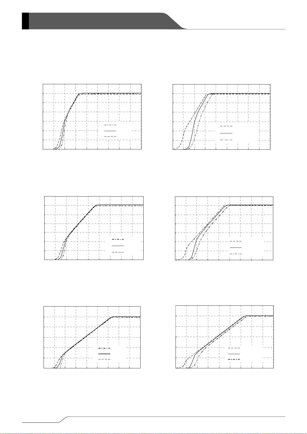
(6) Rising Response Time
XC6224x181
tr=5μs, Ta=25℃, CIN=CL=0.47μF
Input Voltage
Output Voltage
IOUT=1mA
IOUT=30mA
IOUT=100mA
Time [10us/div]
[V]
IN
Input Voltage :V
XC6224x121
4
3
2
1
0
-1
-2
-3
-4
tr=5μs, Ta=25℃, CIN=CL=0.47μF
Input Voltage
Output Voltage
IOUT=1mA
IOUT=30mA
IOUT=100mA
Time [10μs/div]
2.4
2.1
1.8
1.5
1.2
0.9
0.6
0.3
0.0
[V]
OUT
Output Voltage : V
4
3
2
[V]
IN
1
0
-1
Input Voltage : V
-2
-3
-4
XC6224
3.2
2.8
2.4
[V]
OUT
2.0
1.6
1.2
0.8
Output Voltage : V
0.4
0.0
Series
XC6224x251
tr=5μs, Ta=25℃, CIN=CL=0.47μF
4
3
2
[V]
IN
1
0
-1
Input Voltage : V
-2
-3
-4
Time [10us/div]
(7) Input Transient Response
XC6224x121
8.0
7.0
6.0
[V]
IN
5.0
Output Voltage
Input Voltage
Output Volt age
IOUT=1 mA
IOUT=30mA
IOUT=100mA
VIN = 1.7V ⇔ 2.7V, tr=tf=5μs,
=30mA, Ta=25℃, CIN=CL=0.47μF
I
OUT
4.0
3.5
3.0
2.5
2.0
1.5
1.0
0.5
0.0
1.22
1.21
1.20
1.19
[V]
OUT
Output Voltage : V
XC6224x181
V
= 2.30V ⇔ 3.30V, tr=tf=5μs,
IN
I
=30mA, Ta=25℃, CIN=CL=0.47μF
9.0
8.0
[V]
OUT
7.0
[V]
IN
6.0
OUT
Output Voltage
1.82
1.81
1.80
1.79
[V]
OUT
4.0
3.0
Input Voltage: V
2.0
Input Voltage
1.0
0.0
Time [10μs/div]
1.18
1.17
1.16
1.15
1.14
5.0
4.0
Input Voltage: V
Output Voltage : V
3.0
Input Voltage
2.0
1.0
1.78
1.77
1.76
1.75
1.74
Output Voltage: V
Time [10us/div]
13/26

XC6224 Series
■TYPICAL PERFORMANCE CHARACTERISTICS (Continued)
(7) Input Transient Response (Continued)
XC6224x251
VIN = 3.00V ⇔ 3.60V, tr=tf=5μs,
I
=30mA, Ta=25℃, CIN=CL=0.47μF
9.0
OUT
2.52
8.0
Output Voltage
7.0
[V]
IN
6.0
5.0
4.0
Input Voltage V
3.0
Input Voltage
2.0
1.0
Time [10us/div]
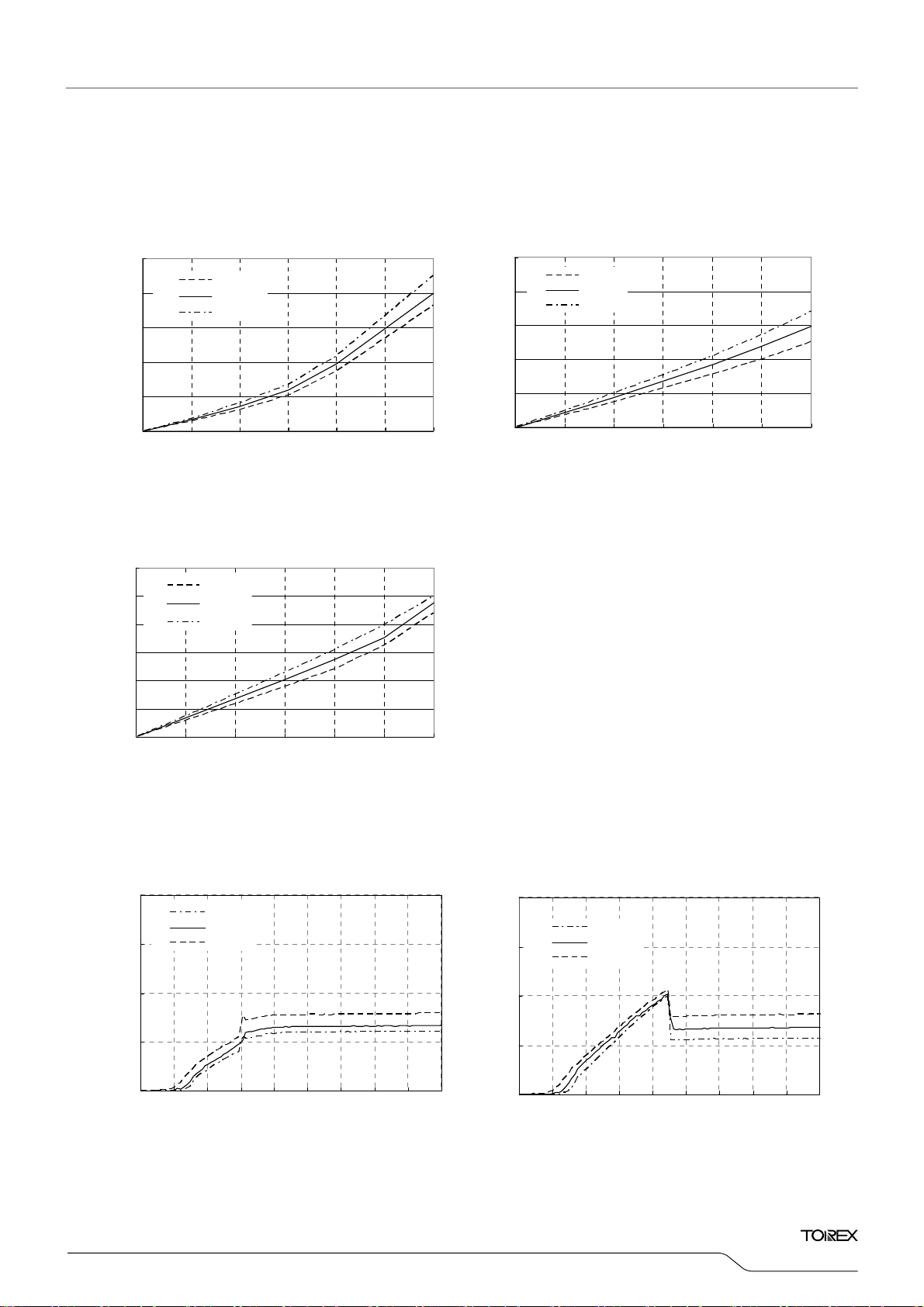
(8) Load Transient Response
XC6224x121
500
450
400
350
[mA]
OUT
300
250
200
150
Output Current: I
100
50
0
Output Voltage
Output Current
Time [10us/div]
I
= 1mA ⇔ 150mA, tr=tf=0.5μs,
OUT
=2.25V, Ta=25℃, CIN=CL=0.47μF
V
IN
2.51
2.50
2.49
2.48
2.47
2.46
2.45
2.44
1.40
1.35
1.30
1.25
1.20
1.15
1.10
1.05
1.00
0.95
0.90
[V]
OUT
Output Voltage V
XC6224x121
I
= 50mA ⇔ 100mA, tr=tf=0.5μs,
OUT
= 2.25V, Ta=25℃, CIN=CL=0.47μF
V
500
450
400
[V]
[mA]
350
OUT
OUT
300
250
200
150
Output Voltage: V
Output Current: I
100
50
0
IN
Output Volt age
Output Current
1.40
1.35
1.30
1.25
1.20
1.15
1.10
1.05
1.00
0.95
0.90
[V]
OUT
Output Voltage: V
Time [10us/div]
[mA]
OUT
Output Current: I
14/26
500
450
400
350
300
250
200
150
100
50
XC6224x181
I
= 1 mA ⇔ 15 0mA, tr =t f=0 .5μs,
OUT
V
= 2.80V, Ta=25℃, CIN=CL=0.47μF
IN
1.95
1.90
1.85
Output Voltage
1.80
1.75
1.70
Output Current
1.65
1.60
1.55
1.50
0
1.45
500
450
400
[V]
350
[mA]
OUT
OUT
300
250
200
150
Output Voltage: V
Output Current: I
100
50
0
Time [10us/div]
XC6224x181
I
= 50mA ⇔ 100mA, tr=tf=0.5μs,
OUT
V
= 2.80V, Ta=25℃, CIN=CL=0.47μF
IN
Output Voltage
Output Current
Time [10us/div]
1.95
1.90
1.85
1.80
1.75
1.70
1.65
1.60
1.55
1.50
1.45
[V]
OUT
Output Voltage: V
■TYPICAL PERFORMANCE CHARACTERISTICS (Continued)
(8) Load Transient Response (Continued)
XC6224
Series
XC6224x251
I
OUT
500
V
450
400
350
[mA]
OUT
300
Output Voltage
250
200
Output Current
150
Output Current: I
100
50
0
Time [10us/div]
(9) CE Rising Response Time
XC6224x121
VCE=0 →1V, tr=tf=5μs, I
V
4.0
3.5
[V]
3.0
OUT
2.5
2.0
1.5
1.0
Output Voltage : V
0.5
0.0
IN
Time [10us/div]
= 1 mA ⇔ 15 0mA, tr=tf= 0.5 μs,
= 3.3 0V, Ta=25 ℃, CIN=CL=0.47μF
IN
= 3 0mA
= 2.25V, Ta=25℃, CIN=CL=0.47μF
CE Input Voltage
Output Voltage
OUT
2.65
2.60
2.55
2.50
2.45
2.40
2.35
2.30
2.25
2.20
2.15
2.0
1.5
1.0
0.5
0.0
-0.5
-1.0
-1.5
-2.0
XC6224x251
I
= 50mA ⇔ 100mA, tr=tf=0.5μs,
OUT
V
= 3.30V, Ta=25℃, CIN=CL=0.47μF
500
450
400
[V]
OUT
350
[mA]
OUT
300
250
200
150
Output Voltage: V
Output Current: I
100
50
0
IN
Output Voltage
Output Current
2.65
2.60
2.55
2.50
2.45
2.40
2.35
2.30
2.25
2.20
2.15
[V]
OUT
Output Voltage: V
Time [10us/div]
XC6224x181
VCE=0 →1V, tr=tf=5μs, IOUT = 30mA
= 2.80V, Ta=25℃, CIN=CL=0.47μF
V
4.0
3.5
[V]
3.0
[V]
CE
OUT
2.5
IN
CE Input Voltage
2.0
1.5
CE Voltage : V
1.0
Output Voltage : V
0.5
Output Voltage
0.0
2.0
1.5
1.0
0.5
0.0
-0.5
-1.0
-1.5
-2.0
[V]
CE
CE Voltage : V
Time [10us/div]
XC6224x251
VCE=0 →1V, tr=tf=5μs, I
V
= 3.50V, Ta=25℃, CIN=CL=0.47μF
4.0
3.5
[V]
3.0
OUT
2.5
2.0
1.5
1.0
Output Voltage: V
IN
CE Input Voltage
Output Voltage
0.5
0.0
OUT
= 3 0mA
2.0
1.5
1.0
0.5
0.0
-0.5
-1.0
-1.5
-2.0
[V]
CE
CE Voltage : V
Time [10us/div]
15/26

XC6224 Series
■TYPICAL PERFORMANCE CHARACTERISTICS (Continued)
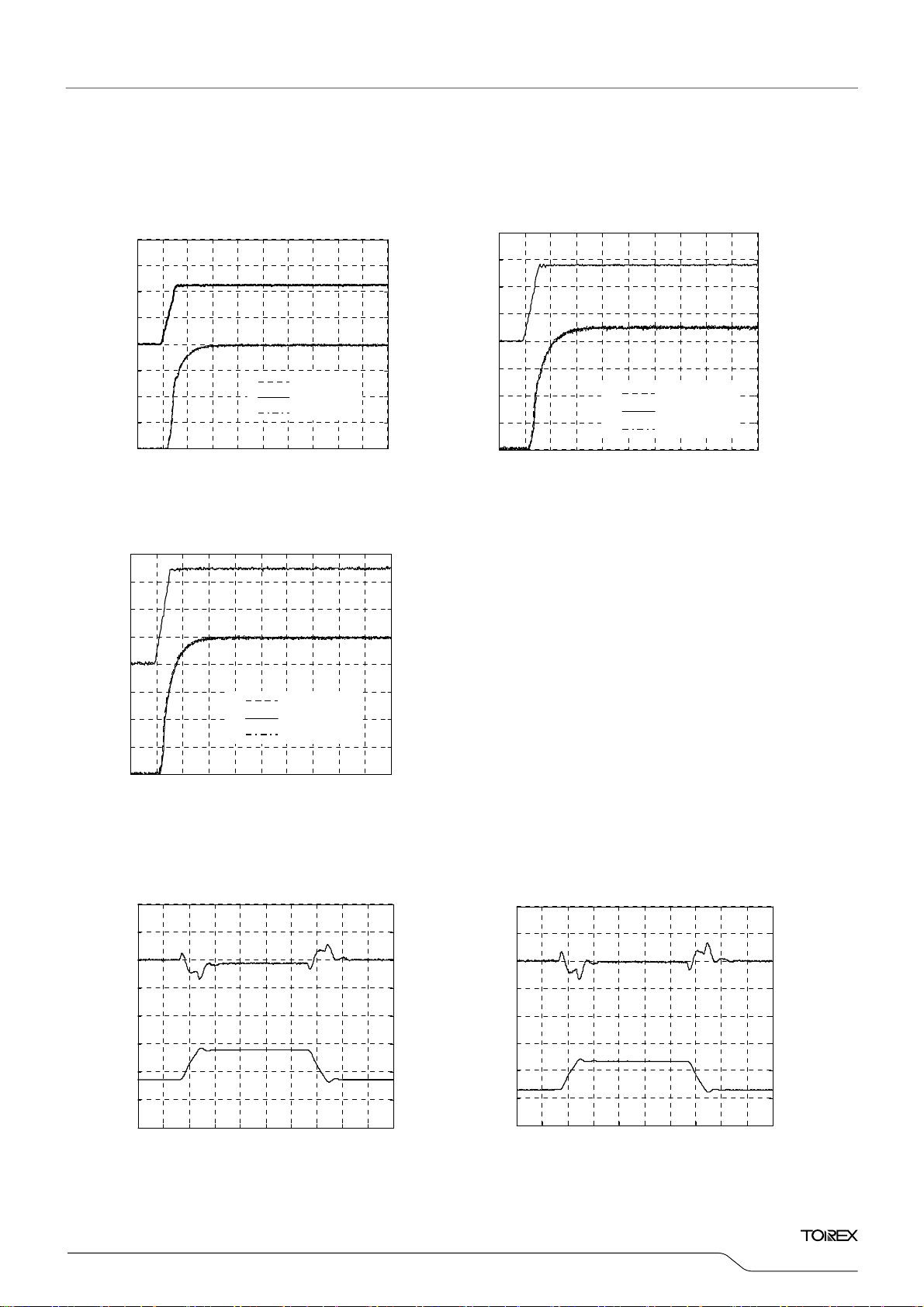
(10) CL Discharge Response Time
XC6224x121
VCE=1 →0V, tr=tf=5μs
V
= 2 .2 V, Ta=25 ℃, CIN=CL=0.47μF
4.0
3.5
3.0
[V]
OUT
2.5
2.0
1.5
Output Voltage : V
1.0
0.5
0.0
IN
CE Input Voltage
Output Voltage
Time [500us/div]
3
2
1
[V]
CE
0
-1
-2
-3
CE Input Voltage : V
-4
-5
4.0
3.5
3.0
[V]
OUT
2.5
2.0
1.5
Output Voltage : V
1.0
0.5
0.0
XC6224x181
VCE=1 →0V, tr=tf=5μs
V
= 2 .8 0V, Ta=2 5℃, CIN=CL=0.47μF
IN
CE Input Voltage
Output Voltage
Time [500us/div]
3
2
1
[V]
CE
0
-1
-2
-3
CE Input Voltage : V
-4
-5
XC6224x251
VCE=1 →0V, tr=tf=5μs,
= 3 .50V, Ta=2 5℃, CIN=CL=0.47μF
V
4.8
4.2
3.6
3.0
IN
CE Input Voltage
3
2
1
0
2.4
1.8
1.2
Output Voltage : VOUT[V]
0.6
0.0
(11) Ripple Rejection Rate
90
80
70
60
50
40
30
20
10
Ripple Rejec tion Rate: RR[dB]
0
100 1k 10k 100k
IOUT=30mA
IOUT=100mA
Output Voltage
Time [500us/div]
XC6224x121
Ta=25℃, VIN=3.0VDC+0.5Vp-p
C=C=0.47μF
Ripple Frequency: f[Hz]
-1
-2
VCE Voltage : VCE[V]
-3
-4
-5
X6224x181
AC
90
80
70
60
50
40
30
20
Ripple Rejection Rate: RR[dB]
10
0
100 1k 10k 100k
IOUT=30mA
IOUT=100mA
Rippl e Fr equen cy: f[Hz ]
Ta=25℃, VIN=3.0VDC+0.5Vp-p
C=C=0.47μF
AC
16/26
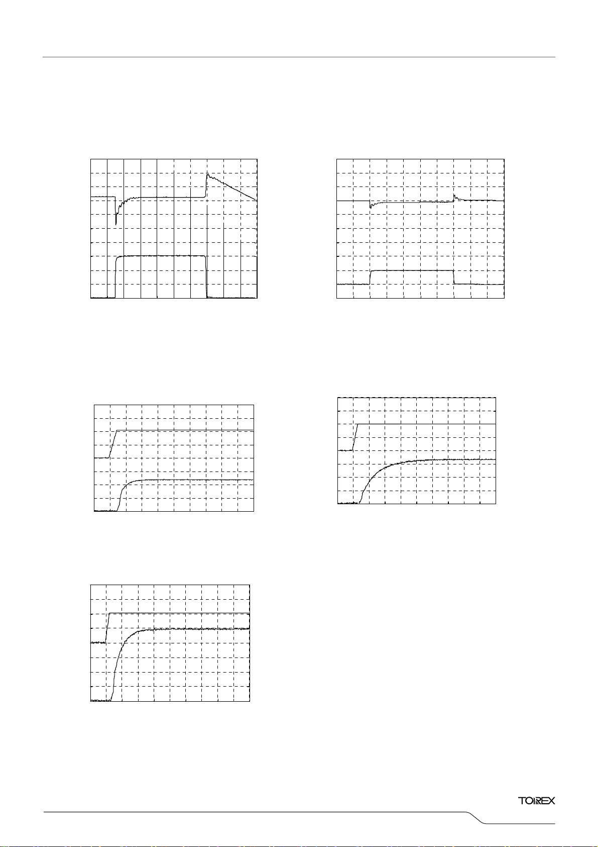
■TYPICAL PERFORMANCE CHARACTERISTICS (Continued)
(11) Ripple Rejection Rate
XC6224
Series
XC6224x251
90
80
70
60
50
40
30
20
10
Ripple Rejec tion Rate: RR[dB]
0
100 1k 10k 100k
IOUT=30mA
IOUT=100mA
Rippl e Fr equen cy: f[Hz ]
Ta=25℃, VIN=3.0VDC+0.5Vp-p
CIN=CL=0.47μF
AC
(12) The Minimum Operating Voltage
2.00
[V]
IN
Input Voltage : V
1.80
1.60
1.40
1.20
1.00
0.80
0.60
0.40
0.20
0.00
0.8V Operation Area
0 30 60 90 120 150
XC6224x081
Output Current : I
Ta=25℃, CIN=CL=0.47μF
[mA]
OUT
* The graph shows minimum input voltages as a function of output current. The vales are influenced by a driver ON resistance.
17/26
XC6224 Series
■PACKAGING INFORMATION
USPN-4B02
(unit : mm)
SOT-25
(unit : mm)
+0.1
0.4
-0.05
+0.02
0.75±0.05
0.95±0.05
-0.03
0.18±0.05
0.38
12
C0.07
43
(0.4)
2.9±0.2
5 4
1
(0.95)
1pin INDENT
0.2±0.05
2
0.325±0.05
+0.2
-0.1
1.6
2.8±0.2
3
0.25
0.25
SSOT-24
(unit : mm)
+0.15
-0.1
+0.15
-0.1
+0.1
0.15
-0.05
2.0±0.1
1.3±0.2
0~0.1
+0.15
0.25
-0.1
+0.1
0
-0
+0.2
-0.1
1.25
2.1±0.3
+0
+0.1
0.125
+0.15
-0.1
0.35
0.05
1.1MAX
0.9±0.1
0.2MIN
-0.05
-0.2
0.3
18/26
1.9±0.2
1.3MAX
1.1±0.1

■PACKAGING INFORMATION (Continued)
●USPN-4B02 Reference Pattern Layout ●USPN-4B02 Reference Metal Mask Design
●USPN-4B02 参考パターンレイアウト
0.14 0.4 0.14
0.23 0.23
●USPN-4B02 参考メタルマスクデザイン
0.18 0.18
0.115 0.4 0.115
XC6224
Series
19/26

)
XC6224 Series
■PACKAGING INFORMATION (Continued
● SSOT-24 Power Dissipation
Power dissipation data for the SSOT-24 is shown in this page.
The value of power dissipation varies with the mount board conditions.
Please use this data as one of reference data taken in the described
condition.
1. Measurement Condition (Reference data)
20/26
Condition: Mount on a board
Ambient: Natural convection
Soldering: Lead (Pb) free
Board: Dimensions 40 x 40 mm (1600 mm
Copper (Cu) traces occupy 50% of the board area
In top and back faces
Package heat-sink is tied to the copper traces
Material: Glass Epoxy (FR-4)
Thickness: 1.6 mm
Through-hole: 4 x 0.8 Diameter
2. Power Dissipation vs. Ambient temperature
Board Mount (Tj max = 125℃)
Ambient Temperature(℃) Power Dissipation Pd(mW) Thermal Resistance (℃/W)
25 500
85 200
Power Dissipation Pd (mW)
2
in one side)
200.00
Evaluation Board (Unit: mm)

)
p
(
)
XC6224
Series
■PACKAGING INFORMATION (Continued
● SOT-25 Power Dissipation
Power dissipation data for the SOT-25 is shown in this page.
The value of power dissipation varies with the mount board conditions.
Please use this data as one of reference data taken in the described
condition.
1. Measurement Condition (Reference data)
Condition: Mount on a board
Ambient: Natural convection
Soldering: Lead (Pb) free
Board: Dimensions 40 x 40 mm (1600 mm
Copper (Cu) traces occupy 50% of the board area
Material: Glass Epoxy (FR-4)
Thickness: 1.6 mm
Through-hole: 4 x 0.8 Diameter
2. Power Dissipation vs. Ambient temperature
Board Mount (Tj max = 125℃)
In top and back faces
Package heat-sink is tied to the copper traces
(Board of SOT-26 is used.)
Ambient Temperature(℃) Power Dissipation Pd(mW) Thermal Resistance (℃/W)
2
in one side)
評価基板レイアウト(単位:mm)
Evaluation Board (Unit: mm)
25 600
85 240
Pd-Ta特性グラフ
Pd vs. Ta
700
mW
600
166.67
500
400
ation Pd
300
200
100
許容損失Pd(mW)
Power Dissi
0
25 45 65 85 105 125
Ambient Temperature Ta (℃)
周辺温度Ta(℃)
21/26

)
p
(
)
XC6224 Series
■PACKAGING INFORMATION (Continued
● USPN-4B02 Power Dissipation
Power dissipation data for the USPN-4B02 is shown in this page.
The value of power dissipation varies with the mount board conditions.
Please use this data as one of reference data taken in the described condition.
1. Measurement Condition (Reference data)
Condition: Mount on a board
Ambient: Natural convection
Soldering: Lead (Pb) free
Board: Dimensions 40 x 40 mm (1600 mm
Material: Glass Epoxy (FR-4)
Thickness: 1.6 mm
Through-hole: 4 x 0.8 Diameter
2. Power Dissipation vs. Ambient temperature
Board Mount (Tj max = 125℃)
Copper (Cu) traces occupy 50% of the front and 50% of the back.
The copper area is divided into four block,
one block is 12.5% of total.
The USPN-4 package has for terminals.
Each terminal connects one copper block in the front
and one in the back.
Ambient Temperature(℃) Power Dissipation Pd(mW) Thermal Resistance (℃/W)
2
in one side)
Evaluation Board (Unit: mm)
25 550
85 220
Pd vs. Ta
600
mW
500
400
ation Pd
300
200
100
許容損失Pd(mW)
Power Dissi
0
25 45 65 85 105 125
Pd-Ta特性グラフ
周囲温度Ta(℃)
Ambient Temperature Ta (℃)
181.82
22/26

■ MARKING RULE
●SOT-25
① represents product series
MARK PRODUCT SERIES
1 XC6224******-G
② represents type of regulator and combination of output voltage
MARK
OUTPUT VOLTAGE
0.1V INCREMENTS
0.8~3.0V 0.85~2.95V
C H XC6224A*****-G
D K XC6224B*****-G
OUTPUT VOLTAGE
0.05V INCREMENTS
③ represents output voltage
OUTPUT VOLTAGE (V) OUTPUT VOLTAGE (V)
MARK
0 0.80 - 0.85 - F 2.30 - 2.35 -
1 0.90 - 0.95 - H 2.40 - 2.45 -
2 1.00 -
3 1.10 - 1.15 - L 2.60 - 2.65 -
4 1.20 - 1.25 - M 2.70 - 2.75 -
5 1.30 - 1.35 - N 2.80 - 2.85 -
6 1.40 - 1.45 - P 2.90 - 2.95 -
7 1.50 - 1.55 - R 3.00 - - -
8 1.60 -
9 1.70 - 1.75 - T - - - -
A 1.80 - 1.85 - U - - - -
B 1.90 - 1.95
C 2.00 - 2.05
D 2.10 - 2.15
E 2.20 - 2.25
0.1V
INCREMENTS
0.05V
INCREMENTS
1.05
1.65
- K
- S - - - -
-
-
-
-
④⑤ represents production lot number
1~09, 0A~0Z, 11・・・9Z, A1~A9, AA・・・Z9, ZA~ZZ repeated.
(G, I, J, O, Q, W excluded.)
* No character inversion used.
54
① ② ③ ④ ⑤
123
PRODUCT SERIES
MARK
V - - - -
X - - - -
Y - - - -
Z - - - -
0.1V
INCREMENTS
2.50
- 2.55 -
0.05V
INCREMENTS
XC6224
Series
23/26

XC6224 Series
■ MARKING RULE (Continued)
●SSOT24 (with bar)
① represents type of regulator and combination of output voltage
MARK
OUTPUT VOLTAGE
0.1V INCREMENTS
VOLTAGE =0.8~2.4V VOLTAGE =2.5~3.0V VOLTAGE =0.85~1.95V VOLTAGE =2.05~2.95V
A F F Z XC6224A*****-G
H P P R XC6224B*****-G
② represents output voltage
MARK
0 0.80 0.85 - 2.05 - F
1 0.90 0.95 - 2.15 - H
2 1.00 1.05 - 2.25 - K
3 1.10 1.15 - 2.35 - L
4 1.20 1.25 - 2.45 - M
5 1.30 1.35 - 2.55 - N
6 1.40 1.45 - 2.65 - P
7 1.50 1.55 - 2.75 - R
8 1.60 1.65 - 2.85 - S
9 1.70 1.75 - 2.95 - T
A 1.80 1.85 - - - U
B 1.90 1.95 - - - V
C 2.00 - 2.50 - - X
D - - - - - Y
E - - - - - Z
③④ represents production lot number
01~09、0A~0Z、11・・・9Z、A1~A9、AA・・・Z9、ZA~ZZ repeated.
(G, I, J, O, Q, W excluded.)
* No character inversion used.
OUTPUT VOLTAGE (V) OUTPUT VOLTAGE (V)
XC6224A/B XC6224A
OUTPUT VOLTAGE
0.05V INCREMENTS
MARK
XC6224A/B XC6224B
- -
- -
- -
- -
- -
2.10 -
- -
- -
- -
- -
2.20 2.60
2.30 2.70
2.40 2.80
- 2.90
- 3.00
PRODUCT
SERIES
- -
- -
- -
- -
- -
2.05 -
2.15 -
2.25
2.35
2.45
2.55
2.65 -
2.75 -
2.85 -
2.95 -
-
-
-
-
3
④
②①
③
2
24/26

■ MARKING RULE (Continued)
●USPN-4B02
① represents type of regulator and combination of output voltage
MARK
OUTPUT VOLTAGE
0.1V INCREMENTS
VOLTAGE =0.8~3.0V VOLTAGE =0.85~2.95V
0 1 XC6224A*****-G
2 3 XC6224B*****-G
② represents output voltage
MARK OUTPUT VOLTAGE (V) MARK OUTPUT VOLTAGE (V)
0 0.80 0.85 F 2.30 2.35
OUTPUT VOLTAGE
0.05V INCREMENTS
XC6224
Series
PRODUCT SERIES
3
④
②①
③
2
1 0.90 0.95 H 2.40 2.45
2 1.00 1.05 K 2.50 2.55
3 1.10 1.15 L 2.60 2.65
4 1.20 1.25 M 2.70 2.75
5 1.30 1.35 N 2.80 2.85
6 1.40 1.45 P 2.90 2.95
7 1.50 1.55 R 3.00 -
8 1.60 1.65 S - -
9 1.70 1.75 T - -
A 1.80 1.85 U - -
B 1.90 1.95 V - -
C 2.00 2.05 X - -
D 2.10 2.15 Y - -
E 2.20 2.25 Z - -
③ represents production lot number
0~9, A~Z repeated.
(G, I, J, O, Q, W excluded.)
* No character inversion used.
25/26
XC6224 Series
1. The products and product specifications contained herein are subject to change without
notice to improve performance characteristics. Consult us, or our representatives
before use, to confirm that the information in this datasheet is up to date.
2. We assume no responsibility for any infringement of patents, patent rights, or other
rights arising from the use of any information and circuitry in this datasheet.
3. Please ensure suitable shipping controls (including fail-safe designs and aging
protection) are in force for equipment employing products listed in this datasheet.
4. The products in this datasheet are not developed, designed, or approved for use with
such equipment whose failure of malfunction can be reasonably expected to directly
endanger the life of, or cause significant injury to, the user.
(e.g. Atomic energy; aerospace; transport; combustion and associated safety
equipment thereof.)
5. Please use the products listed in this datasheet within the specified ranges.
Should you wish to use the products under conditions exceeding the specifications,
please consult us or our representatives.
6. We assume no responsibility for damage or loss due to abnormal use.
7. All rights reserved. No part of this datasheet may be copied or reproduced without the
prior permission of TOREX SEMICONDUCTOR LTD.
26/26
 Loading...