


)
XC6220 Series
ETR0341-010a
1A LDO Voltage Regulator with “GreenOperation”
☆GreenOperation-Compatible
■GENERAL DESCRIPTION
The XC6220 series is a highly accurate, low noise, high speed, low dropout, and large current CMOS voltage regulator with
GreenOperation function. The series consists of a voltage reference, an error amplifier, a current limiter, an inrush current
prevention circuit and a phase compensation circuit plus a driver transistor.
With a 0.2Ω on-resistance driver transistor integrated, the ultra low dropout voltage performance with output currents up to 1A
greatly extends battery life as does the GreenOperation function which can switch between high speed and power save modes
automatically. A low ESR ceramic capacitor can be used for the output stabilization capacitor (C
Output voltage is selectable in 0.05V increments within the range of 0.8V~5.0V, using laser trimming technologies.
An over current protection circuit and a thermal shutdown circuit are built in. The over current protection circuit will operate
when the output current reaches its limit current. The thermal shutdown circuit will operate when the junction temperature
reaches its limit temperature. The inrush prevention circuit works by controlling the inrush current which charges to C
the IC starts up. In this way, voltage fluctuations in power supply caused by inrush current during system start up can be
minimized.
The CE function enables the output to be turned off and the IC becomes a stand-by mode resulting in greatly reduced power
consumption.
■APPLICATIONS
●CD-ROM, CD-R/RW drives
●DVD drives
●HDD drives
●MIDs, UMPCs
●Digital still cameras, Video cameras
●Portable AV equipment
■TYPICAL APPLICATION CIRCUIT
■FEATURES
Maximum Output Current
Dropout Voltage
Operating Voltage Range
Output Voltage Range
Accuracy
Low Power Consumption
Operating Ambient Temperature
Thermal Shutdown
Inrush Current Prevention
C
Auto Discharge
L
CE Pull-Down Resistor
Output Capacitor
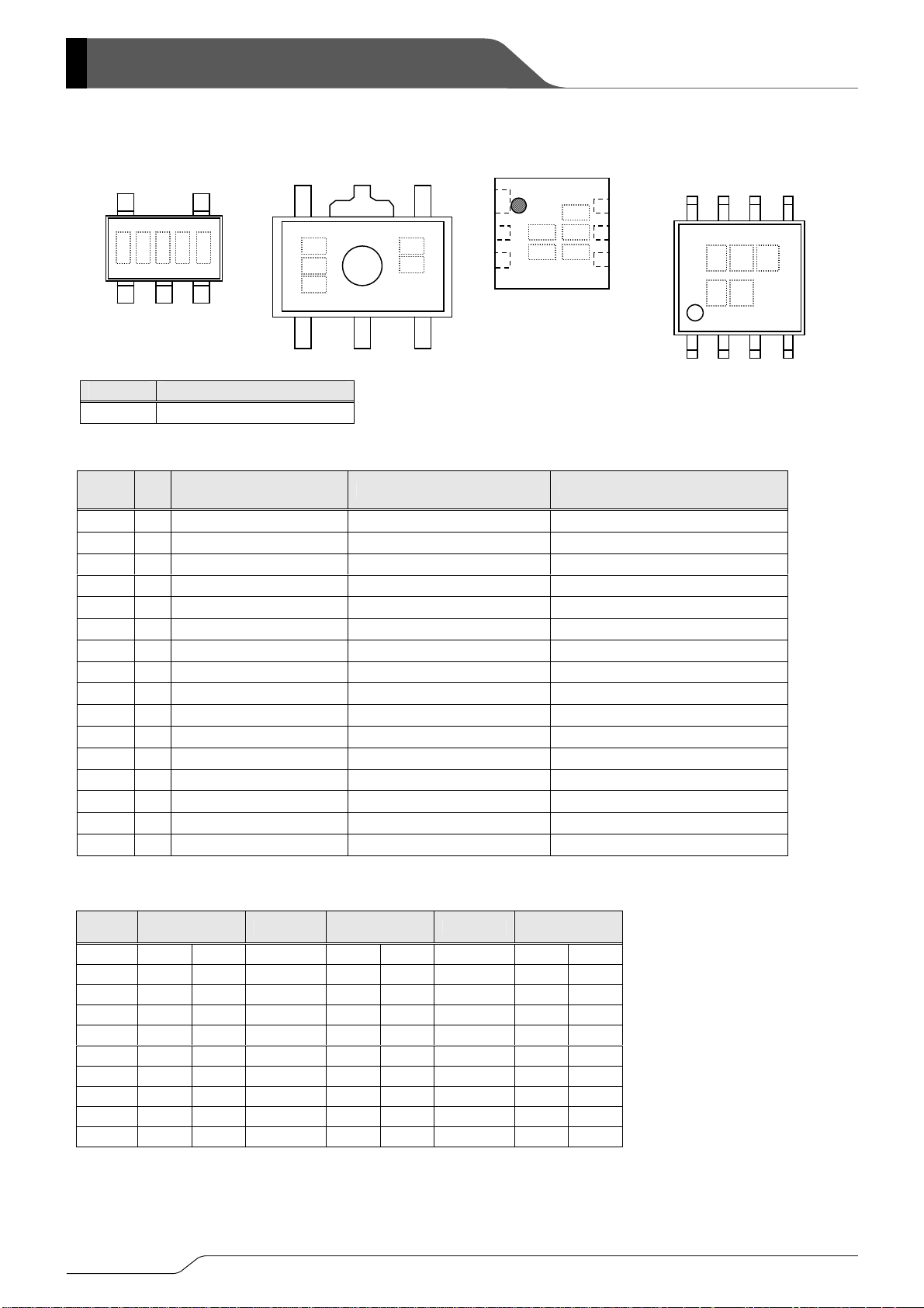
Packages
Environmentally Friendly
■
TYPICAL PERFORMANCE
CHARACTERISTICS
XC6220x181
500
400
300
200
100
Dro pou t V olt age : Vdif (mV)
0
0 200 400 600 800 1000
Topr=25℃
Topr=-40℃
Topr=85℃
Output Current: I
).
L
when
L
:
1000mA (1.2V≦V
: 20mV @ 100mA (V
: 60mV@ 300mA (V
OUT
OUT
OUT
≦5.0V)
=3.0V)
=3.0V)
: 1.6V ~ 6.0V
: 0.8V ~ 5.0V (0.05V increments)
:±1% (V
:±20mV (V
OUT
OUT
≧2.0V)
<2.0V)
: 8μA (TYP.) in PS mode
: 50μA (TYP.) in HS mode
: - 40℃~ +85℃
: Detect 150℃, Release 135℃(TYP.)
: 700mA (MAX.)
: XC6220 Series B/D type
: XC6220 Series C/D type
: Ceramic Capacitor Compatible
:
USP-6C, SOT-25, SOT-89-5
SOP-8FD(Under Development)
: EU RoHS Compliant, Pb Free
CE=VIN, CIN=CL=10μF (ceramic
(mA)
OUT
1/31

XC6220 Series
■PIN CONFIGURATION
■PIN ASSIGNMENT
(Under Development)
* For the USP-6C, the No.5 and 6 V
and 2 pins V
solder-plated in reference mount pattern and metal masking so as to
enhance mounting strength and heat release. If the pad needs to be
connected to other pins, it should be connected to the V
*For the SOP-8FD, two power input pins (No.7 and No.8) output pins (No.1
and 2) should be connected. The dissipation pad should be solder-plated
in electrically open or connecting to the V
pins should be connected. The dissipation pad should be
OUT
pins should be connected. The No.1
IN
(No. 4) pin.
SS
(No.4) pin.
SS
PIN NUMBER
SOT-25 SOT-89-5 USP-6C
SOP-8FD
(Under
Development)
PIN NAME FUNCTIONS
3 1 3 5 CE ON/OFF Control
1 4 6 & 5 7,8 VIN Power Input
2 2 4 4 VSS Ground
5 5 1 & 2 1,2 V
Output
OUT
4 3 - 3,6 NC No connection
■CE PIN LOGIC CONDITION
PIN NAME DESIGNATOR CONDITIONS IC OPERATION
CE
L
H
VCE≦0.4V
1.2V≦VCE≦6.0V
OPEN VCE=OPEN
(*1)
(XC6220A/B Series)
OFF
ON
Undefined state
OFF(XC6220C/D Series)
(*1) Please avoid the state of OPEN, and connect CE pin to any arbitrary voltage.
* For the XC6220C/D series, CE function logic is fixed as L level because of the CE pull-down resister.
2/31
■FUNCTIONS
PRODUCT NAME
XC6220A
XC6220B
XC6220C
XC6220D
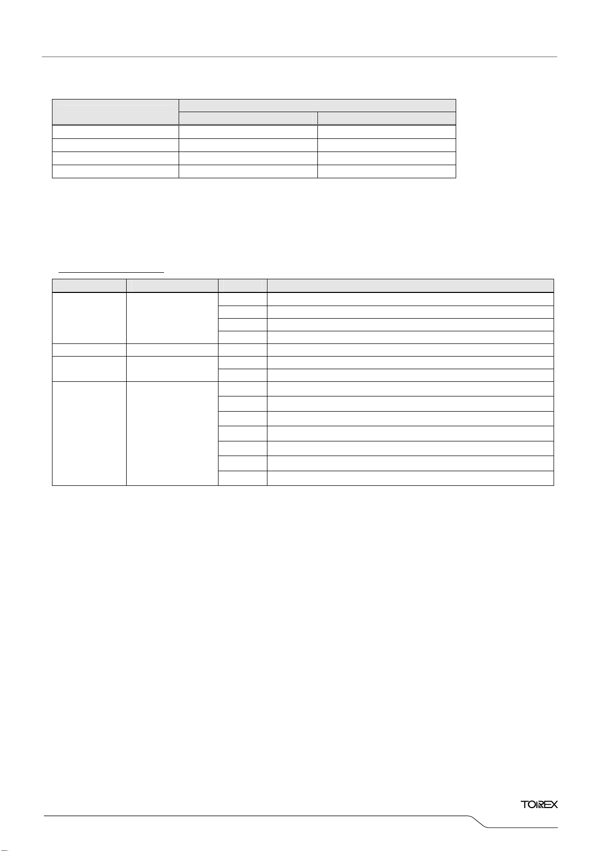
■PRODUCT CLASSIFICATION
●Ordering Information
XC6220 ①②③④⑤⑥-⑦
CE PULL-DOWN RESISTOR CL AUTO DISCHARGE
Not Available Not Available
Not Available Available
Available Not Available
Available Available
(*1)
IC FUNCTION
DESIGNATOR ITEM SYMBOL DESCRIPTION
A without CE Pull-down resistor, without CL discharge (Semi-custom)
① Type of CE
B without CE Pull-down resistor, with CL discharge (Standard)
C with CE Pull-down resistor, without CL discharge (Semi-custom)
D with CE Pull-down resistor, with C
②③ Output Voltage 08~50 e.g. 3.0V → ①=3, ②=0
④
Output Voltage
( the 2nd decimal place)
1 Output voltage {○.○0v} (the 2nd decimal place is “0”)
B
Output voltage {○.○5v} (the 2
nd
MR SOT-25 (3,000/Reel)
MR-G SOT-25 (3,000/Reel)
PR SOT-89-5 (1,000/Reel)
⑤⑥-⑦
Packages
(Order Unit)
PR-G SOT-89-5 (1,000/Reel)
ER USP-6C (3,000/Reel)
ER-G USP-6C (3,000/Reel)
QR-G SOP-8FD (1,000/Reel)
(*1)
The “-G” suffix denotes Halogen and Antimony free as well as being fully RoHS compliant.
(Under Development)
discharge (Semi-custom)
L
decimal place is “5”)
XC6220
Series
3/31
XC6220 Series
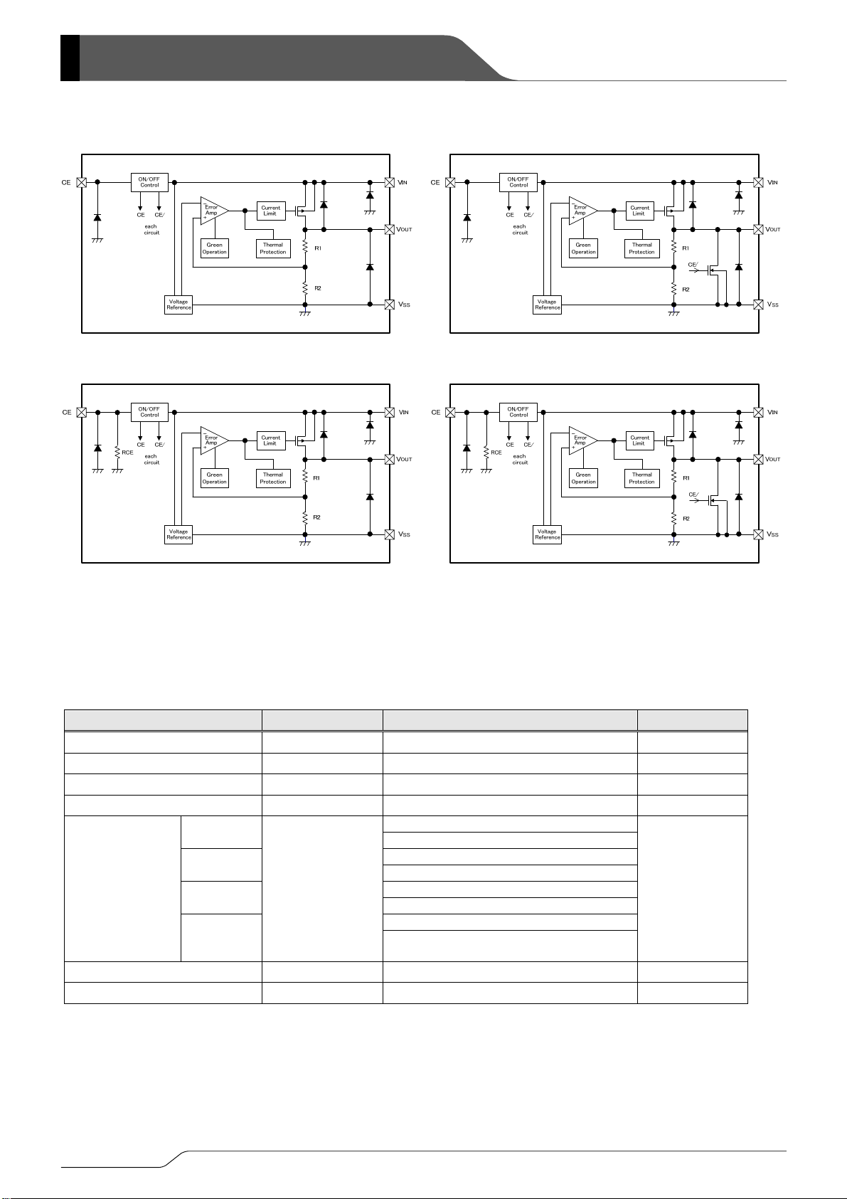
■BLOCK DIAGRAMS
●XC6220 Series Type A (Semi-custom) ●XC6220 Series Type B
●XC6220 Series Type C (Semi-custom) ●XC6220 Series Type D (Semi-custom)
* Diodes inside the circuits are ESD protection diodes and parasitic diodes.
■ABSOLUTE MAXIMUM RATINGS
PAR AMETER SYMBOL RATINGS UNITS
Input Voltage
Output Current
Output Voltage
CE Input Voltage
(*1)
V
V
IN
I
1400 mA
OUT
V
V
OUT
V
V
CE
SOT-25
SOT-89-5
Power Dissipation
USP-6C
Pd
SOP-8FD
(Under
Development)
Operating Ambient Temperature
Storage Temperature
Topr - 40 ~ + 85 ℃
Tstg - 55 ~ + 125 ℃
-0.3 ~ +6.5 V
SS
-0.3 ~ VIN +0.3 V
SS
-0.3 ~ 6.5 V
SS
250
600 (PCB mounted)
500
1300 (PCB mounted)
120
1000 (PCB mounted)
(*2)
(*2)
(*2)
300
(*2)
1500 (PCB mounted)
Ta =2 5℃
mW
*1 Please use within the range of Pd>(VIN – V
*2: The power dissipation figure shown is PCB mounted. Please refer to pages 26~29 for details.
OUT
)×I
OUT
4/31

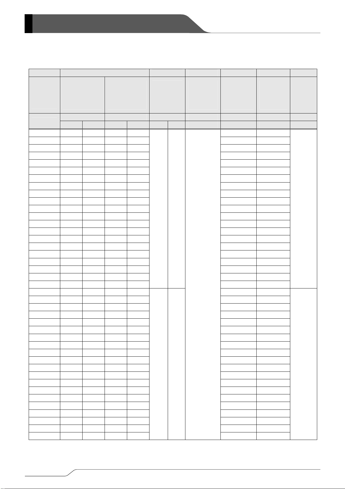
■ELECTRICAL CHARACTERISTICS
●XC6220A/B/C/D Series
PAR AMETER SYMBOL CONDITIONS MIN. TYP. MAX. UNITS CIRCUIT
High Speed Mode (HS)
2.0V≦V
V
CE=VIN
OUT(T)
, I
OUT
≦5.0V
=30mA
×0.99 ×1.01
High Speed Mode (HS)
OUT(T)
, I
OUT
OUT(T)
, I
OUT
≦1.95V
=30mA
≦5.0V
=0.1mA
-0.02 +0.02
(*2)
V
OUT(T)
V ①
×0.98 ×1.02
Output Voltage
V
OUT(E)
(*1)
0.8V≦V
V
CE=VIN
Power Save Mode (PS)
2.0V≦V
V
CE=VIN
Power Save Mode (PS)
0.8V≦V
V
CE=VIN
OUT(T)
, I
OUT
≦1.95V
=0.1mA
-0.04
+0.04
XC6220
Series
Ta =2 5℃
Output Current I
Load Regulation ΔV
Dropout Voltage1 Vdif
Dropout Voltage2 Vdif
Supply Current 1 I
Supply Current 2 I
Stand-by Current I
Line Regulation
Input Voltage VIN
Output Voltage
Temperature
Characteristics
OUTMAX
SS1
SS2
STBY
ΔV
(ΔV
・
IN
ΔV
(ΔTa ・V
VCE=VIN
+1.0V
OUT(T)
≦1.15V
700 1200 -
mA ①
V
IN=VOUT(T)
0.8V≦V
VCE=VIN
1000 1200 -
- 10 45 mV ①
OUT
(*3)
I
(*3)
I
V
IN=VOUT(T)
1.2V≦V
+1.0V
OUT(T)
≦5.0V
High Speed Mode (HS),
V
OUT
OUT
10mA≦I
CE=VIN,
=300mA, VCE=VIN - E-1 mV ①
=1000mA, VCE=VIN - - E-2 mV ①
≦300mA
OUT
High Speed Mode(HS)
V
IN=VCE=VOUT(T)
I
=10mA (A/B Series)
OUT
High Speed Mode(HS)
V
IN=VCE=VOUT(T)
=10mA (C/D Series)
I
OUT
+1.0V
+1.0V
- 50 108
μA ②
- 50 E-3
Power Save Mode(PS)
V
IN=VCE=VOUT(T)
I
=0.1mA (A/B Series)
OUT
Power Save Mode(PS)
V
IN=VCE=VOUT(T)
I
=0.1mA (C/D Series)
OUT
+1.0V
+1.0V
- 8 18
μA ②
- 8 E-4
VIN=6.0V, VCE=VSS -0.1 0.01 0.1 μA ②
V
+0.5V≦VIN≦6.0V
OUT(T)
OUT
V
OUT
1.1V≦V
V
CE=VIN, IOUT
/
)
OUT
1.6V≦V
0.8V≦V
V
CE=VInm, IOUT
V
CE=VIN
/
I
OUT
)
OUT
-40℃≦Ta ≦85℃
=30mA
OUT(T)
≦6.0V
IN
OUT(T)
≦5.0V
=100mA
≦1.05V
=100mA
- 0.01 0.20 %/V ①
1.6 - 6.0 V ①
- ±100 - ppm/℃ ①
5/31

XC6220 Series
■ELECTRICAL CHARACTERISTICS (Continued)
PAR AMETER SYMBOL CONDITIONS MIN. TYP. MAX. UNITS CIRCUIT
VIN=5.75VDC+0.5Vp-pAC
4.75V≦V
V
CE=VIN, IOUT
≦5.0V
OUT(T)
=30mA、f=1kHz
Ta =2 5℃
Ripple Rejection Ratio PSRR
Limit Current I
Short Current I
PS Switching Current I
SHORT
GOR
HS Switching Current IGO
Switch Current
Hysteresis Range
I
GOhys
PS Switching Delay Time t
(*4)
V
V
CEH
I
R
DCHG
CE High Level Voltage
CE Low Level Voltage
CE High Level Current I
CE Low Level Current
CL Discharge Resistance
VIN={V
0.85V≦V
V
V
V
V
VCE=VIN= V
LIM
V
0.8V≦V
1.2V≦V
V
Short V
:1.45V≦V
V
:0.8V≦V
V
I
OUT
:1.45V≦V
V
:0.8V≦V
V
I
OUT
I
GOhys=IGO-IGOR
V
DPS
Time until HS mode is changed-over to
PS mode by I
CEH
CEL
CEL
1.2 - 6.0 V ④
- - 0.4 V ④
VCE=VIN=6.0V(A/B series) -0.1 - 0.1 μA
V
V
VIN=6.0V, V
+1.0}VDC+0.5Vp-pAC
OUT(T)
≦4.7V
OUT(T)
CE=VIN, IOUT
=1.85VDC+0.5Vp-pAC
IN
OUT(T)
CE=VIN,IOUT
CE=VIN
CE=VIN
IN=VOUT(T)
=1.6V, VCE=VIN
IN
=30mA、f=1kHz
=0.8V
=30mA、f=1kHz
OUT(T)
≦1.15V
OUT(T)
= V
OUT(T)
≦5.0V
OUT(T)
to VSS level
OUT
≦5.0V
OUT(T)
+1.0V, VCE=VIN
≦1.4V
OUT(T)
+1.0V
+1.0V
- 50 - dB ③
705 1200 -
mA ①
1005 1200 -
- 180 - mA ①
1.0 2.0 - mA ⑤
=heavy to light load
≦5.0V
OUT(T)
IN=VOUT(T)
=1.6V, VCE=VIN
IN
+1.0V, VCE=VIN
≦1.4V
OUT(T)
- 5.0 10 mA ⑤
=light to heavy load
- 3.0 - mA ⑤
IN=VOUT(T)
+1.0V, V
= V
CE
IN
- - E-5 μs ⑤
GOR.
=6.0V (C/D series) - 9 15 μA
CE=VIN
-0.1 - 0.1 μA ④
CE=VSS
=5.0V, VCE= VSS - 460 - Ω ①
OUT
④
Thermal Shutdown
Detect Temperature
Thermal Shutdown
Release Temperature
Inrush Current I
T
Junction Temperature - 150 - ℃ ①
TSD
T
Junction Temperature - 135 - ℃ ①
TSR
RUSH
V
IN=VOUT(T)
V
CE
+1.0V、CL=22μF
=0V→V
OUT(T)
+1.0V
- - 700 mA ⑥
(Only when rising and within 1ms)
* 1: V
* 2: V
* 3: Vdif = {V
* 4: For the XC6220B/D series only. The XC6220A/C series (semi-custom) discharges by only R1 and R2 resistors as shown in the block diagrams.
= Effective output voltage
OUT (E)
(The output voltage when an amply stabilized "V
= Nominal output voltage. (Shown in the voltage chart E-0)
OUT (T)
V
is the input voltage when V
IN1
V
is the voltage equal to 98% of the HS mode output voltage when an amply stabilized V
OUT1
IN1-VOUT1
}
appears at the V
OUT1
+1.0V" is provided at the VIN pin while maintaining a certain I
OUT (T)
pin while input voltage is gradually decreased.
OUT
OUT
+1.0V are supplied to the VIN pin.
OUT (T)
value.)
6/31

)
■ELECTRICAL CHARACTERISTICS (Continued
●Voltage Chart 1
XC6220
Series
Ta =2 5℃
SYMBOL
NOMINAL
OUTPUT
VOLTAGE
(V)
V
OUT(T)
0.80 0.7800 0.8200 0.7600 0.8400
0.85 0.8300 0.8700 0.8100 0.8900 112.625
0.90 0.8800 0.9200 0.8600 0.9400 112.750
0.95 0.9300 0.9700 0.9100 0.9900
1.00 0.9800 1.0200 0.9600 1.0400
1.05 1.0300 1.0700 1.0100 1.0900
1.10 1.0800 1.1200 1.0600 1.1400
1.15 1.1300 1.1700 1.1100 1.1900
1.20 1.1800 1.2200 1.1600 1.2400
OUTPUT
VOLTAGE 1
(HS Mode)
(V)
V
OUT
MIN. MAX. MIN. MAX.
E-0 E-1 E-2 E-3 E-4 E-5
OUTPUT
VOLTAGE 2
(PS Mode)
V
(V)
OUT
DROPOUT
VOLTAGE 1
Vdif 1 (mV)
I
=300mA
OUT
TYP.
400
V
dif1
MAX.
575
240 405
180 305
DROPOUT
VOLTAGE 2
Vdif 2 (mV)
I
=1000mA
OUT
V
I
dif2
SUPPLY
CURRENT 1
(XC6220C/D )
(μA)
SS1
MAX. MAX. MAX.
112.500 22.500
-
112.875
113.000 23.000
113.125 23.125
113.250 23.250
113.375 23.375
113.500 23.500
1.25 1.2300 1.2700 1.2100 1.2900 113.625
1.30 1.2800 1.3200 1.2600 1.3400 113.750
1.35 1.3300 1.3700 1.3100 1.3900 113.875
150
215 460
1.40 1.3800 1.4200 1.3600 1.4400 114.000
1.45 1.4300 1.4700 1.4200 1.4800
1.50 1.4800 1.5200 1.4700 1.5300
1.55 1.5300 1.5700 1.5100 1.5900
1.60 1.5800 1.6200 1.5600 1.6400
1.65 1.6300 1.6700 1.6100 1.6900
1.70 1.6800 1.7200 1.6600 1.7400
1.75 1.7300 1.7700 1.7100 1.7900
1.80 1.7800 1.8200 1.7600 1.8400
1.85 1.8300 1.8700 1.8100 1.8900
1.90 1.8800 1.9200 1.8600 1.9400
1.95 1.9300 1.9700 1.9100 1.9900
2.00 1.9800 2.0200 1.9600 2.0400
2.05 2.0295 2.0705 2.0090 2.0910
2.10 2.0790 2.1210 2.0580 2.1420
2.15 2.1285 2.1715 2.1070 2.1930
2.20 2.1780 2.2220 2.1560 2.2440
2.25 2.2275 2.2725 2.2050 2.2950
2.30 2.2770 2.3230 2.2540 2.3460
2.35 2.3265 2.3735 2.3030 2.3970
2.40 2.3760 2.4240 2.3520 2.4480
2.45 2.4255 2.4745 2.4010 2.4990
2.50 2.4750 2.5250 2.4500 2.5500
2.55 2.5245 2.5755 2.4990 2.6010
100 150
85 130
655
114.125
114.250 24.250
114.375 24.375
114.500 24.500
114.625 24.625
114.750 24.750
114.875 24.875
115.000 25.000
115.125 25.125
115.250 25.250
115.375 25.375
115.500 25.500
115.625 25.625
115.750 25.750
115.875 25.875
116.000 26.000
116.125 26.125
116.250 26.250
116.375 26.375
116.500 26.500
116.625 26.625
116.750 26.750
116.875 26.875
2.60 2.5740 2.6260 2.5480 2.6520 117.000
2.65 2.6235 2.6765 2.5970 2.7030 117.125
2.70 2.6730 2.7270 2.6460 2.7540 117.250
2.75 2.7225 2.7775 2.6950 2.8050 117.375
65 110
2.80 2.7720 2.8280 2.7440 2.8560 117.500
2.85 2.8215 2.8785 2.7930 2.9070
2.90 2.8710 2.9290 2.8420 2.9580
2.95 2.9205 2.9795 2.8910 3.0090
117.625 27.625
117.750 27.750
117.875 27.875
SUPPLY
CURRENT 2
(XC6220C/D )
I
22.625
22.750
22.875
23.625
23.750
23.875
24.000
24.125
27.000
27.125
27.250
27.375
27.500
(μA)
t
SS2
PS
SWITCH
DELAY
TIME
(μs)
DPS
MAX.
650
850
1200
7/31
)
XC6220 Series
■ELECTRICAL CHARACTERISTICS (Continued
●Voltage Chart 2
SYMBOL
NOMINAL
OUTPUT
VOLTAGE
(V)
V
OUT(T)
3.00 2.9700 3.0300 2.9400 3.0600
3.05 3.0195 3.0805 2.9890 3.1110
3.10 3.0690 3.1310 3.0380 3.1620
3.15 3.1185 3.1815 3.0870 3.2130
3.20 3.1680 3.2320 3.1360 3.2640
3.25 3.2175 3.2825 3.1850 3.3150
3.30 3.2670 3.3330 3.2340 3.3660
3.35 3.3165 3.3835 3.2830 3.4170
3.40 3.3660 3.4340 3.3320 3.4680
3.45 3.4155 3.4845 3.3810 3.5190
3.50 3.4650 3.5350 3.4300 3.5700
3.55 3.5145 3.5855 3.4790 3.6210
3.60 3.5640 3.6360 3.5280 3.6720
3.65 3.6135 3.6865 3.5770 3.7230
3.70 3.6630 3.7370 3.6260 3.7740
3.75 3.7125 3.7875 3.6750 3.8250
3.80 3.7620 3.8380 3.7240 3.8760
3.85 3.8115 3.8885 3.7730 3.9270
3.90 3.8610 3.9390 3.8220 3.9780
3.95 3.9105 3.9895 3.8710 4.0290
4.00 3.9600 4.0400 3.9200 4.0800
4.05 4.0095 4.0905 3.9690 4.1310
4.10 4.0590 4.1410 4.0180 4.1820
4.15 4.1085 4.1915 4.0670 4.2330
4.20 4.1580 4.2420 4.1160 4.2840
4.25 4.2075 4.2925 4.1650 4.3350
4.30 4.2570 4.3430 4.2140 4.3860
4.35 4.3065 4.3935 4.2630 4.4370
4.40 4.3560 4.4440 4.3120 4.4880
4.45 4.4055 4.4945 4.3610 4.5390
4.50 4.4550 4.5450 4.4100 4.5900
4.55 4.5045 4.5955 4.4590 4.6410
4.60 4.5540 4.6460 4.5080 4.6920
4.65 4.6035 4.6965 4.5570 4.7430
4.70 4.6530 4.7470 4.6060 4.7940
4.75 4.7025 4.7975 4.6550 4.8450
4.80 4.7520 4.8480 4.7040 4.8960
4.85 4.8015 4.8985 4.7530 4.9470
4.90 4.8510 4.9490 4.8020 4.9980
4.95 4.9005 4.9995 4.8510 5.0490
5.00 4.9500 5.0500 4.9000 5.1000
OUTPUT
VOLTAGE
(HS Mode)
(V)
V
OUT
MIN. MAX. MIN.
E-0 E-1 E-2 E-3 E-4 E-5
OUTPUT
VOLTAGE
(PS Mode)
V
DROPOUT
VOLTAGE 1
Vdif 1 (mV)
(V)
OUT
MAX. TYP. MAX.
I
OUT
60 95
53 85
=300mA
V
dif1
DROPOUT
VOLTAGE 2
Vdif 2 (mV)
I
=1000mA
OUT
V
dif2
MAX. MAX.
655
SUPPLY
CURRENT 1
(XC6220C/D)
(μA)
I
I
SS1
118.000 28.000
118.125 28.125
118.250 28.250
118.375 28.375
118.500
118.625
118.750
118.875
119.000
119.125
119.250 29.250
119.375 29.375
119.500 29.500
119.625 29.625
119.750
119.875
120.000
120.125
120.250
120.375
120.500 30.500
120.625 30.625
120.750 30.750
120.875 30.875
121.000 31.000
121.125 31.125
121.250 31.250
121.375 31.375
121.500 31.500
121.625 31.625
121.750 31.750
121.875 31.875
122.000 32.000
122.125 32.125
122.250 32.250
122.375 32.375
122.500 32.500
122.625 32.625
122.750 32.750
122.875 32.875
123.000 33.000
SUPPLY
CURRENT 2
(XC6220C/D)
(μA)
SS2
MAX.
28.500
28.625
28.750
28.875
29.000
29.125
29.750
29.875
30.000
30.125
30.250
30.375
Ta =2 5℃
PS
SWITCH
DELAY
TIME
(μs)
t
DPS
MAX.
1200
1450
8/31
)
XC6220
Series
■OPERATIONAL EXPLANATION
CE V
RCE
ON/OFF
Control
CE CE/
each
circuit
Voltage
Reference
-
Error
Amp
+
Green
Operation
Current
Limit
Thermal
Protection
R1
CE/
R2
<GreenOperation>
The XC6220 series always operates in a green operation (GO) mode.
The GO mode enables the IC to switch automatically between the high
speed (HS) mode or the power save (PS) mode according to the level of
output current. The switching point of the HS mode and the PS mode is
fixed inside the IC. When the output current becomes I
or below, the mode changes automatically to the PS mode after a delay
time of hundreds of microseconds. Supply current in light load is greatly
reduced. Also when the output current becomes I
more, the mode changes automatically to the HS mode and the IC
returns to high speed operation.
GOR
10mA (MAX.) or
GO
<Low ESR capacitor>
The XC6220 series has a built-in phase compensation circuit which means that a stable output voltage is achieved even if
the IC is used with low ESR capacitors. In order to ensure stable phase compensation it is recommended that a C
is connected as close as possible to the V
(CIN) between the VIN pin and the VSS pin.
Values required for the phase compensation are shown in the chart below. If a loss of the capacitance happens, the stable
phase compensation may not be obtained. Please ensure to use a capacitor which does not depend on bias or temperature
too much.
<Current Limiter, Short-Circuit Protection>
The XC6220 series includes a fold-back circuit, which aids the operation of the current limiter and circuit protection. When
the load current reaches the current limit level, the fold-back circuit operates and output voltage drops. As a result of this drop
in output voltage, output current also decreases. When the output pin is shorted, a current of about 180mA flows.
<CE Pin>
The IC's internal circuitry can be shutdown via the signal from the CE pin with the XC6220 series. With the XC6220A/C
series, output at the V
N-channel transistor switch is connected in parallel to R1 and R2 while the power supply is applied to the V
the time until the V
unstable, when the CE pin is open. If this IC is used with the correct output voltage for the CE pin, the logic is fixed and the
IC will operate normally. On the other hand, with the XC6220C/D series, the IC operation is stopped when the CE pin is
open. However, the CE pin input current may increase as a result of through current in the pull-down resistor (R
IC is under operation.
Recommended output capacitor (C
V
(V)
OUT(T)
0.80V~0.95V
1.00V~1.45V 47μF 47μF 22μF
1.50V~1.75V 47μF 22μF 10μF
1.80V~2.95V 47μF 6.8μF 6.8μF
3.00V~3.50V 47μF 4.7μF 4.7μF
3.55V~5.00V 47μF 10μF 6.8μF
× No option
pin will be pulled down to the VSS level. However, with XC6220B/D series, the CL auto-discharge
OUT
pin reaches the VSS level is shortened. The output voltage of the XC6220A/B series becomes
OUT
CIN=4.7μF CIN=10μF CIN=22μF
pin and VSS pin. For a stable power supply, please connect an input capacitor
OUT
)
L
OUTPUT CAPACITOR VALUE(CL)
× ×
The voltage divided by resistors R1 & R2 is compared
with the internal reference voltage by the error amplifier.
IN
The P-channel MOSFET which is connected to the V
pin is then driven by the subsequent control signal. The
output voltage at the V
V
OUT
by a system of negative feedback. The current limit
pin is controlled & stabilized
OUT
circuit and short protect circuit operate in relation to the
level of output current. The GO function monitors the
output current and switches the IC between two
operating modes according to the level of output
V
SS
current. Further, the IC's internal circuitry can be
shutdown via the CE pin's signal.
XC6220x301
CE=VIN, Topr=25℃, CIN=10μF, CL=4. 7μF (cer ami c
Output Current: I
(mA)
OUT
=1.0mA (MIN.)
50
40
30
20
Supply Current: ISS (μA)
10
0
0 5 10 15 20
22μF
pin. Therefore,
IN
OUT
capacitor
L
) when the
CE
9/31

XC6220 Series
■OPERATIONAL EXPLANATION (Continued)
<CL Discharge Function>
The XC6220B/D series can quickly discharge the electric charge at the output capacitor (CL) via the N-channel transistor
located between the V
put into an OFF state (cf. BLOCK DIAGRAM).
pin voltage) ÷ (N-channel transistor through current) = CL discharge resistance (R
(V
OUT
auto-discharge resistance value is fixed to 460Ω(VIN=6.0V, V
The C
L
capacitor (C
) is set by the CL auto-discharge resistance (R
L
the CL auto-discharge resistance value [R
after discharge via the N-channel transistor is calculated by the following formulas.
where
V : Output voltage after discharge
V
: Output voltage
OUT(E)
t: Discharge time
auto-discharge resistance R
τ: C
L
<Inrush Current Prevention>
The XC6220 series includes an inrush current Prevention circuit.
The inrush current protection circuit suppresses inrush current charged to C
approximately 1ms.
* Please note that the device can not provide the output current beyond 700 mA for a period of approximately 1ms after the
CE pin goes high.
OUT pin and the VSS pin, when a low signal is inputted to the CE pin, which enables the whole IC circuit
)
DCHG
=5.0V at TYP.). The discharge time of the output
OUT
) and the output capacitor (CL). By setting a time constant of
x e
DCHG
–t/
τ
, or t=τln( V
), the output voltage
DCHG
/ V )
OUT(E)
when the IC starts up to 700 mA (MAX.) for
L
] and an output capacitor value (CL) as τ(τ=C x R
DCHG
V = V
OUT(E)
×Output capacitor (CL) value C)
DCHG
■NOTES ON USE
1. For temporary, transitional voltage drop or voltage rising phenomenon, the IC is liable to malfunction should the ratings be
exceeded.
2. Where wiring impedance is high, operations may become unstable due to noise and/or phase lag depending on output
current. Please strengthen V
3. Please wire the input capacitor (C
4. As for the XC6220A/C series (semi-custom), the output voltage may float with a leakage current of the driver transistor
between V
and V
IN
and R1+R2 resistance while stand-by (operation stop). Please take consideration of this and check it
OUT
before use.
5. Torex places an importance on improving our products and their reliability. We request that users incorporate fail-safe
designs and post-aging protection treatment when using Torex products in their systems.
and VSS wiring in particular.
IN
) and the output capacitor (CL) as close to the IC as possible.
IN
10/31

■TEST CIRCUITS
Circuit 1: Output Voltage, Output Current, Dropout Voltage, Input Voltage, Line Regulation, Load Regulation,
Current Limit, Short Current, C
・測定回路1 (出力電圧・出力電流・入出力電圧差・入力動作電圧・入力安定度・負荷安定度・制限電流・
Thermal Shutdown Detect Temperature, Thermal Shutdown Release Temperature
短絡電流・CL放電抵抗)
Discharge Resistance, Output Voltage Temperature,
L
VIN
VOUT
A
SW
2
V
CIN
(ceramic)
SW1
CE
VSS
CL
(ceramic)
IOUT
V
RL
Circuit 2: Supply Current, Stand-by Current
スタ ン バ イ・測定回路2(消費電流・ 電流)
A
VIN
VOUT
A
SW2
CIN
(ceramic)
SW1
CE
VSS
A
CL
(ceramic)
Circuit 3: Ripple Rejection Ratio
・測定回路3(リップル除去率)
IOUT=
30mA
VIN
VOUT
A
V
CE
VSS
CL
(ceramic)
V
RL
PS:0.1mA
HS:10mA
XC6220
Series
11/31

XC6220 Series
■TEST CIRCUITS (Continued)
Circuit 4: CE “H” Level Voltage, CE“L” Level Voltage, CE “H” Level Current, CE “L” Level Current
Circuit 5: HS Switching Current, PS Switching Current, Switch Current Hysteresis Range, PS Switching Delay Time
Circuit 6: Inrush Current
・測定回路4 (CE” H” L” レベル 電圧・ CE” H” L”レベル電流)
CIN
(ceramic)
VCE
VIN
A
CE
V
VSS
VOUT
CL
(ceramic)
・測定回路5 (HS切替電流、PS切替電流、切替ヒステリシス電流、PS切替遅延時間)
VOUT
ISS
CIN
(ceramic)
VIN
CE
VSS
A
・測定回路6(突入電流防止)
A
V
VCE
VIN
CE
VOUT
VSS
CL
(ceramic)
V
V
CL
IOUT
A
RL
=22uF
12/31

)
)
)
)
)
)
■TYPICAL PERFORMANCE CHARACTERISTICS
(1) Output Voltage vs. Output Current
1.4
1.2
(V)
1
OUT
0.8
0.6
XC6220x121
CE= VIN, Topr=25℃, CIN=CL=22μF (ceramic
1.4
1.2
(V)
1
OUT
0.8
0.6
0.4
Output Voltage: V
0.2
0
0 0.2 0.4 0.6 0.8 1 1.2 1.4
Output Current: I
OUT
(A)
VIN=1.6V
VIN=2.2V
0.4
Output Voltage: V
0.2
0
0 0.2 0.4 0.6 0.8 1 1.2 1.4
3.5
3
(V)
2.5
OUT
2
1.5
XC6220x301
CE= VIN, Topr=25℃, CIN=10μF, CL=4.7μF (ceramic
3.5
3
(V)
2.5
OUT
2
1.5
1
Output Voltage: V
0.5
0
0 0.2 0.4 0.6 0.8 1 1.2 1.4
Output Current: I
OUT
(A)
VIN=3.1V
VIN=4.0V
1
Output Voltage: V
0.5
0
0 0.2 0.4 0.6 0.8 1 1 .2 1 .4
6
XC6220x501
CE= VIN, Topr=25℃, CIN=CL=10μF (ceramic
6
5
(V)
4
OUT
5
(V)
4
OUT
3
2
Output Voltage: V
1
0
0 0.2 0.4 0 .6 0 .8 1 1.2 1 .4
Output Current: I
OUT
(A)
VIN=5.1V
VIN=6.0V
3
2
Output Voltage: V
1
0
0 0.2 0.4 0.6 0.8 1 1.2 1.4
XC6220x121
VIN=CE=2.2V, CIN=CL=22μF (ceramic
Output Current: I
OUT
(A)
XC6220x301
VIN=CE=4.0V, CIN=10μF, CL=4.7μF (ceramic
Output Current: I
OUT
(A)
XC6220x501
VIN=CE=6.0V, CIN=CL=10μF (ceramic
Output Current: I
OUT
(A)
XC6220
Series
Topr=25℃
Topr=-40℃
Topr=85℃
Topr=25℃
Topr=-40℃
Topr=85℃
Topr=25℃
Topr=-40℃
Topr=85℃
13/31

)
)
)
)
)
XC6220 Series
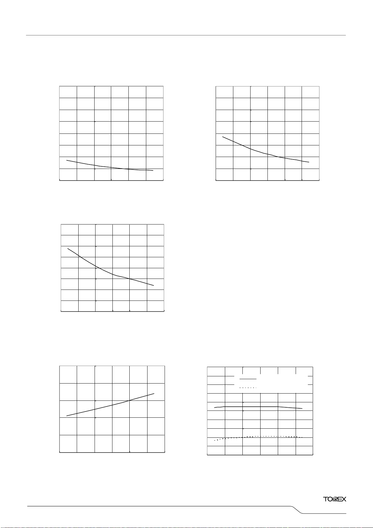
■TYPICAL PERFORMANCE CHARACTERISTICS (Continued)
(2) Output Voltage vs. Input Voltage
1.4
1.2
1
(V)
OUT
0.8
0.6
0.4
Output Voltage: V
0.2
0
0123456
6
5
(V)
4
OUT
3
2
Output Voltage: V
1
0
0123456
(3) Dropout Voltage vs. Output Current
600
500
400
300
200
Dropout Voltage: Vdif (mV)
100
0
0 200 400 600 800 1000
XC6220x121
CE= VIN, Topr=25℃, CIN=CL=22μF (ceramic
Input Voltage: V
XC6220x501
CE=VIN, Topr=25℃, CIN=CL=10μF (ceramic
Input Voltage: V
XC6220x121
CE=VIN, Topr=25℃, CIN=CL=22μF (ceramic
Topr=25℃
Topr=-40℃
Topr=85℃
Output Current: I
14/31
OUT
IN
(V)
(V)
IN
(mA)
IOUT=0.1mA
IOUT=30mA
IOUT=100mA
IOUT=0.1mA
IOUT=30mA
IOUT=100mA
3.5
3
2.5
(V)
OUT
2
1.5
1
Output Voltage: V
0.5
0
0123456
600
500
400
300
200
Dropout Voltage: Vdif (mV)
100
0
0 200 400 600 800 1000
XC6220x301
CE=VIN, Topr=25℃, CIN=10μF, CL=4.7μF (cerami c
IOUT=0.1mA
IOUT=30mA
IOUT=100mA
Input Voltage: V
(V)
IN
XC6220x301
CE=VIN, Topr=25℃, CIN=10μF, CL=4.7μF (cerami c
Topr=25℃
Topr=-40℃
Topr=85℃
Output Current: I
OUT
(mA)

)
)
)
)
■TYPICAL PERFORMANCE CHARACTERISTICS (Continued)
(3) Dropout Voltage vs. Output Current
600
XC6220x501
CE= VIN, Topr=25℃, CIN=CL=10μF (ceramic
500
400
Topr=25℃
Topr=-40℃
Topr=85℃
300
200
Dropout Voltage: Vdif (mV)
100
0
0 200 400 600 800 1000
Output Current: I
OUT
(mA)
(4) Output Voltage vs. Ambient Temperature
1.224
XC6220x121
VIN=CE=2.2V, I
CIN=CL=22μF (ceramic
OUT
=30mA,
3.06
XC6220x301
VIN=CE=4.0V, I
C
=10μF, CL=4.7μF (cerami c
IN
1.212
(V)
OUT
(V)
OUT
3.03
1.2
3
1.188
Output Voltage: V
Output Voltage: V
2.97
1.176
-50 -25 0 25 50 75 100
Ambient Temperature: Tpor (℃)
XC6220x501
5.1
VIN=CE=6.0V, I
C
=10μF (ceramic
IN=CL
OUT
=30mA,
2.94
-50 -25 0 25 50 75 100
Ambient Temperature: Tpor (℃)
5.05
(V)
OUT
5
4.95
Output Voltage: V
4.9
-50 -25 0 25 50 75 100
Ambient Temperature: Tpor (℃)
OUT
=30mA,
XC6220
Series
15/31

A
)
A
)
)
A
)
A
)
)
XC6220 Series
■TYPICAL PERFORMANCE CHARACTERISTICS (Continued)
(5) Supply Current vs. Input Voltage
Supply Current: ISS (μA)
Supply Current: ISS (μA)
Supply Current: ISS (μA)
16/31
XC6220x121
CE=VIN, I
=0.1m
OUT
Topr=25℃
90
80
CIN=CL=22μF (ceramic
Topr=-40℃
70
Topr=85℃
60
50
40
30
20
10
0
0123456
Input Voltage: V
IN
(V)
XC6220x301
CE= VIN, I
=0.1mA
OUT
90
80
70
Topr=25℃
Topr=-40℃
Topr=85℃
C
=10μF, CL=4.7μF (cerami c
IN
60
50
40
30
20
10
0
0123456
Input Voltage: V
(V)
IN
XC6220x501
CE=VIN, I
=0.1m
90
CIN=CL=10μF (ceramic
80
70
Topr=25℃
Topr=-40℃
Topr=85℃
60
50
40
30
20
10
0
0123456
Input Voltage: V
(V)
IN
OUT
90
80
70
60
50
40
30
Supply Current: ISS (μA)
20
10
0
0123456
90
80
70
60
50
40
30
20
Supply Current: ISS (μA)
10
0
0123456
90
80
70
60
50
40
30
Supply Current: ISS (μA)
20
10
0
0123456
XC6220B121
Input Voltage: V
XC6220x301
Topr=25℃
Topr=-40℃
Topr=85℃
Input Voltage: V
XC6220x501
Topr=25℃
Topr=-40℃
Topr=85℃
Input Voltage: V
CIN=CL=22μF (ceramic
Topr=25℃
Topr=-40℃
Topr=85℃
(V)
IN
CIN=10μF, CL=4.7μF (cerami c
(V)
IN
(V)
IN
CE=VIN, I
CE=VIN, I
C
IN=CL
=10m
OUT
=10m
OUT
CE= VIN, I
OUT
=10μF (ceramic
=10mA
)
)
)
)
)
■TYPICAL PERFORMANCE CHARACTERISTICS (Continued)
(6) PS Switching Delay Time vs. Ambient Temperature
1600
XC6220x121
VIN=CE=2.2V, I
C
IN=CL
=10mA→0.1mA
OUT
=22μF (ceramic
1600
XC6220x301
VIN=CE=4.0V, I
=10μF, CL=4. 7μF (ce ramic
C
IN
1400
1200
1400
1200
1000
800
TDPS (μs)
600
400
TDPS (μs)
1000
800
600
400
200
0
-50 -25 0 25 50 75 100
Ambient Temperature: Tpor (℃)
200
0
-50 -25 0 25 50 75 100
Ambient Temperature: Tpor (℃)
1600
1400
XC6220x501
VIN=CE=6.0V, I
C
=10mA→0.1mA
OUT
=10μF (ceramic
IN=CL
1200
1000
800
TDPS (μs)
600
400
200
0
-50 -25 0 25 50 75 100
(7)
CL Discharge Resistance v
Ambient Temperature: Tpor (℃)
s. Ambient Temperature
(8) PS/HS Switch Current vs. Ambient Temperature
700
600
500
400
Rdischg (Ω)
300
200
-50 -25 0 25 50 75 100
XC6220B/D
VIN=6.0V, CE=VSS, V
C
=10μF, CL=4.7μF (ceramic
IN
Ambient Temperature: Tpor (℃)
=5.0V
OUT
XC6220x301
VIN=CE=4.0V, CIN=10μF, CL=4. 7μF (ce ramic
10
9
8
7
(mA)
OUT
6
HS Switching Current
PS Switching Current
5
4
3
Input Current: I
2
1
0
-50 -25 0 25 50 75 100
Ambient Temperature: Tpor (℃)
=10mA→0.1mA
OUT
XC6220
Series
17/31

)
)
)
)
)
)
XC6220 Series
■TYPICAL PERFORMANCE CHARACTERISTICS (Continued)
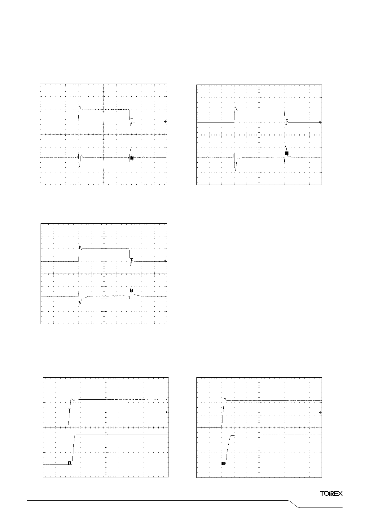
(9) Load Transient Response
CH1
Output Voltage
300mA
Output Current
0.1mA
CH2
VIN=CE=2.2V, Tr=T f=5μs
Topr=25℃, C
=22μF (ceramic
IN=CL
CH1
CH2
10mA
300mA
Topr=25℃, C
Output Voltage
Output Current
VIN=CE=2.2V, Tr=T f=5μs
IN=CL
=22μF (ceramic
CH1
CH2
0.1mA
200μs/div
CH1:100mV/div CH2:100mA/div
Topr=25℃, C
VIN=CE=4.0V, Tr=T f=5μs
=10μF, CL=4.7μF (cerami c
IN
300mA
Output Current
200μs/div
CH1:100mV/div CH2:100mA/div
XC6220x501
VIN=CE=6.0V, Tr=Tf=5μs
Topr=25℃, C
=10μF (ceramic
IN=CL
CH1
CH2
200μs/div
CH1:100mV/div CH2:100mA/div
XC6220x301
Output Voltage
300mA
Output Current
10mA
200μs/div
CH1:100mV/div CH2:100mA/div
Topr=25℃, C
VIN=CE=4.0V, Tr=Tf=5μs
=10μF, C
=4.7μF (cerami c
VIN=CE=6.0V, Tr=T f=5μs
Topr=25℃, C
=10μF (ceramic
IN
CH1
CH2
18/31
0.1mA
Output Voltage
200μs/div
CH1
CH2
10mA
Output Voltage
300mA
Output Current
200μs/div
CH1:100mV/div CH2:100mA/div
A
)
A
)
)
A
)
)
■TYPICAL PERFORMANCE CHARACTERISTICS (Continued)
(10) Line Transient Response
CE= VIN, Tr=Tf=5μs, I
Topr=25℃, CIN=CL=22μF (ceramic
OUT
=100m
XC6220x301
CE= VIN, Tr=Tf=5μs, I
Topr=25℃, CIN=10μF, CL=4.7μF (cerami c
CH1
2.2V
Input Voltage
3.2V
CH1
4.0V
5.0V
Input Voltage
CH2
Output Voltage
CH2
Output Voltage
CH1:1V/div CH2:20mV/div
100μs/div
CH1:1V/div CH2:20mV/div
100μs/div
CE=VIN, Tr=Tf=5μs, I
Topr=25℃, C
IN=CL
=100mA
OUT
=22μF (ceramic
CH1
5.5V
Input Voltage
6.0V
CH2
Output Voltage
(11) Input Rise Characteristics
CH1:500mV/div CH2:20mV/div
100μs/div
CE=VIN, Tr=5μs, I
Topr=25℃, CL=22μF (ceramic
=0.1m
OUT
CE= VIN, Tr=5μs, I
Topr=25℃, C
2.2V
Input Voltage
Input Voltage
CH1
0V
Output Voltage
CH1
0V
Output Voltage
CH2
CH2
200μs/div
200μs/div
=100m
OUT
=300mA
OUT
=22μF (ceramic
L
XC6220
Series
19/31

A
)
A
)
A
)
A
)
A
)
A
)
XC6220 Series
■TYPICAL PERFORMANCE CHARACTERISTICS (Continued)
(11) Input Rise Characteristics
4.0V
CH1
0V
CH2
CH1:2V/div CH2:2V/div
CH1
CH2
CH1:2V/div CH2:2V/div
(12) CE Rise Characteristics
CH1
CH2
CH1:500mV/div CH2:500mV/div
20/31
Input Voltage
Output Voltage
200μs/div
Input Voltage
200μs/div
CE Voltage
Output Voltage
100μs/div
CE=VIN, Tr=5μs, I
Topr=25℃, CL=4.7μF (cerami c
CE= VIN, Tr=5μs, I
Topr=25℃, CL=22μF (ceramic
OUT
OUT
Output Voltage
VIN=2.2V, Tr=5μs , I
Topr=25℃, CIN=CL=22μF (ceramic
OUT
=0.1m
=0.1m
=0.1m
CH1
CH2
CH1
CH2
CH1
CH2
0V
0V
4.0V
Input Voltage
Output Voltage
200μs/div
CH1:2V/div CH2:2V/div
6.0V
Input Voltage
200μs/div
CH1:2V/div CH2:2V/div
CE Voltage
100μs/div
CH1:500mV/div
CH2:500mV/div
CE=VIN, Tr=5μs, I
Topr=25℃, CL=4.7μF (cerami c
CE= VIN, Tr=5μs, I
Topr=25℃, CL=22μF (ceramic
Output Voltage
VIN=2.2V, Tr=5μs , I
Topr=25℃, CIN=CL=22μF (ceramic
Output Voltage
OUT
OUT
OUT
=300m
=300m
=300m

)
A
)
A
)
A
)
)
)
■TYPICAL PERFORMANCE CHARACTERISTICS (Continued)
(12) CE Rise Characteristics
Topr=25℃, C
VIN=4.0V, Tr=5μs , I
=10μF, CL=4.7μF (cerami c
IN
OUT
=0.1mA
Topr=25℃, CIN=10μF, CL=4.7μF (cerami c
VIN=4.0V, Tr=5μs , I
CE Voltage
CE Voltage
CH1
Output Voltage
CH1
Output Voltage
CH2
CH2
CH1:500mV/div CH2:1V/div
100μs/div
XC6220x501
Topr=25℃, CIN=CL=10μF (cer am ic
VIN=6.0V, Tr=5μs , I
OUT
CH1:500mV/div
=0.1m
100μs/div
CH2:1V/div
VIN=6.0V, Tr=5μs , I
Topr=25℃, CIN=CL=10μF (ceramic
CE Voltage
CE Voltage
CH1
Output Voltage
CH1
Output Voltage
CH2
CH2
(13) Inrush Current
100μs/div
CH1:500mV/div CH2:2V/div
CH1:500mV/div CH2:2V/div
100μs/div
Topr=25℃, C
VIN=2.2V, Tr=5μs
=22μF (ceramic
IN=CL
Topr=25℃, C
=10μF, C
CE Voltage
CE Voltage
CH1
CH2
Output Voltage
CH1
CH2
Output Voltage
CH3
Inrush Current
CH3
Inrush Current
CH1:500mV/div CH2:1V/div CH3:100mA/div
100μs/div
CH1:500mV/div CH2:1V/div CH3:100mA/div
100μs/div
XC6220
=300m
OUT
=300m
OUT
VIN=4.0V, Tr=5μs
=4.7μF (cerami c
21/31
Series

)
A
)
A
)
)
A
)
XC6220 Series
■TYPICAL PERFORMANCE CHARACTERISTICS (Continued)
(13) Inrush Current
CE Voltage
CH1
CH2
CH3
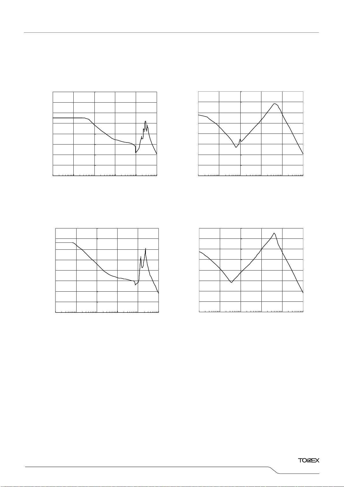
(14)
CH1:500mV/div CH2:1V/div CH3:100mA/div
CL Discharge Time
CH1
CH2
CH1:500mV/div CH2:2V/div
(15) Ripple Rejection Ratio
XC6220x121 (HighSpeed mode)
80
70
60
50
40
30
20
Ripple Rejection Ratio: RR (dB)
10
0
0.01 0.1 1 10 100 1000
22/31
Topr=25℃, C
Output Voltage
100μs/div
XC6220x301 (B/D)
Topr=25℃, CIN=10μF, CL=4.7μF (cerami c
2.0ms/div
VIN=CE=2.2VDC+0.5Vp-pAC, I
Topr=25℃, C
Ripple Frequency: f (kHz)
=0.1μF, CL=22μF (ceramic
IN
VIN=6.0V, Tr=5μs
=10μF (ceramic
IN=CL
Inrush Current
VIN=4.0V, Tf=5μs, I
CE Voltage
Output Voltage
OUT
OUT
=30mA
=0.1m
XC6220x301 (A/C)
Topr=25℃, CIN=10μF, CL=4.7μF (cerami c
CH1
CH2
200ms/div
CH1:500mV/div CH2:2V/div
XC6220x121 (PowerSave mode)
80
Topr=25℃, CIN=0.1μF, CL=22μF (ceramic
70
60
50
40
30
20
Ripple Rejection Ratio: RR (dB)
10
0
0.01 0.1 1 10 100 1000
Ripp;e Frequency: f (kHz)
VIN=4.0V, Tf=5μs, I
CE Voltage
Output Voltage
VIN=CE=2.2VDC+0.5Vp-pAC, I
=0.1m
OUT
=0.1m
OUT
A
)
)
)
A
)
■TYPICAL PERFORMANCE CHARACTERISTICS (Continued)
(15) Ripple Rejection Ratio
XC6220x301 (HighSpeed mode)
VIN=CE=4.0VDC+0.5Vp-pAC, I
80
70
60
50
Topr=25℃, CIN=0.1μF, CL=4.7μF (cerami c
=30m
OUT
XC6220x301 (PowerSave mode)
VIN=CE=4.0VDC+0.5Vp-pAC, I
80
70
60
50
Topr=25℃, C
=0.1μF, CL=4.7μF (cerami c
IN
40
30
40
30
20
Ripple Rejection Ratio: RR (dB)
10
0
0.01 0.1 1 10 100 1000
Ripple Frequency: f (kHz)
20
Ripple Rejection Ratio: RR (dB)
10
0
0.01 0.1 1 10 100 1000
Ripple Frequency: f (kHz)
XC6220x501 (HighSpeed mode)
XC6220c501 (HighSpeed mode)
VIN=CE=5.5.0VDC+0.5Vp-pAC, I
80
Topr=25℃, C
70
=30mA
=0.1μF, CL=10μF (ceramic
IN
OUT
XC6220x501 (PowerSave mode)
VIN=CE=5.5.0VDC+0.5Vp-pAC, I
80
70
Topr=25℃, CIN=0.1μF, CL=10μF (ceramic
60
50
40
30
20
Ripple Rejection Ratio: RR (dB)
10
0
0.01 0.1 1 10 100 1000
Ripple Frequency: f (kHz)
60
50
40
30
20
Ripple Rejection Ratio: RR (dB)
10
0
0.01 0.1 1 10 100 1000
Ripple Frequency: f (kHz)
XC6220
Series
=0.1mA
OUT
=0.1m
OUT
23/31

XC6220 Series
■PACKAGING INFORMATION
●USP-6C
●SOT-89-5
0.42±0.06
5
4.5±0.1
+0.15
1.6
-0.2
0.42±0.06
2
0.42±0.06
4
●SOT-25
●SOP-8FD
(Under Development)
+0.03
0.4
-0.02
0.4 MIN
123
0.42±0.06 0.42±0.060.47±0.06
8°
1.5±0.1 1.5±0.1
24/31
Φ1.0
8°
6.0±0.2
3.9±0.1
+0.03
0.4
-0.02
(1.45)
1.55±0.2
0~0.11
(2.4)

)
■PACKAGING INFORMATION (Continued
●USP-6C Reference Pattern Layout ●USP-6C Reference Metal Mask Design
2.4
0.45
0.45
XC6220
Series
1
0.225
0.50.5
2
3
0.05
0.05
1.0
6
0.25
5
0.250.25
1.8
4
25/31
XC6220 Series
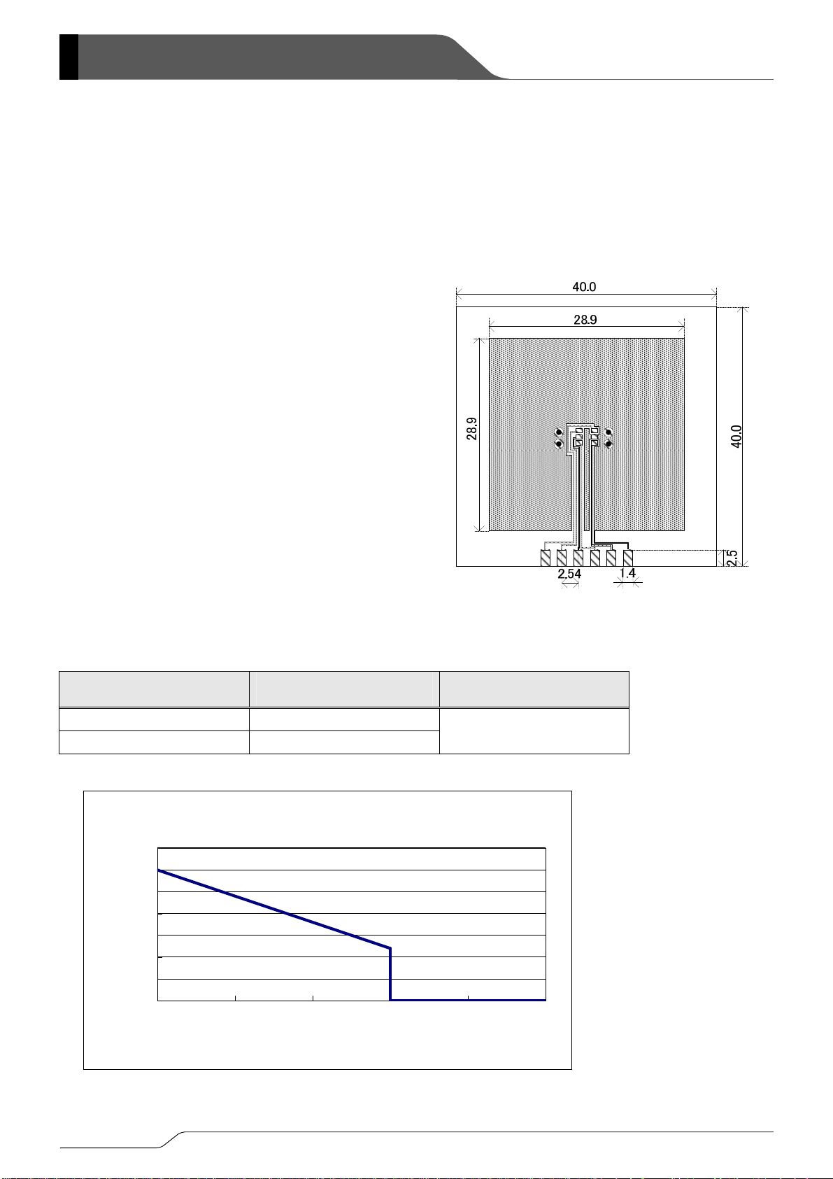
■PACKAGING INFORMATION (Continued)
● SOT-25 Power Dissipation
Power dissipation data for the SOT-25 is shown in this page.
The value of power dissipation varies with the mount board conditions.
Please use this data as one of reference data taken in the described condition.
1. Measurement Condition (Reference data)
Condition: Mount on a board
Ambient: Natural convection
Soldering: Lead (Pb) free
Board: Dimensions 40 x 40 mm (1600 mm
Copper (Cu) traces occupy 50% of the board area
In top and back faces
Package heat-sink is tied to the copper traces
(Board of SOT-26 is used.)
Material: Glass Epoxy (FR-4)
Thickness: 1.6 mm
Through-hole: 4 x 0.8 Diameter
2
in one side)
2. Power Dissipation vs. Ambient temperature
Board Mount (Tj max = 125℃)
Evaluation Board (Unit: mm)
評価基板レイアウト(単位:mm)
Ambient Temperature(℃) Power Dissipation Pd(mW) Thermal Resistance (℃/W)
25 600
166.67
85 240
Pd-Ta特性グラフ
Pd vs. Ta
700
600
500
400
300
200
100
許容損失Pd(mW)
Power Dissipation Pd (mW)
0
25 45 65 85 105 125
Ambient Temperature Ta (℃)
周辺温度Ta(℃)
26/31

XC6220
Series
■PACKAGING INFORMATION (Continued)
● SOT-89-5 Power Dissipation
Power dissipation data for the SOT-89-5 is shown in this page.
The value of power dissipation varies with the mount board conditions.
Please use this data as one of reference data taken in the described condition.
2. Measurement Condition (Reference data)
Condition: Mount on a board
Ambient: Natural convection
Soldering: Lead (Pb) free
Board: Dimensions 40 x 40 mm (1600 mm
Copper (Cu) traces occupy 50% of the board area
In top and back faces
Package heat-sink is tied to the copper traces
Material: Glass Epoxy (FR-4)
Thickness: 1.6 mm
Through-hole: 5 x 0.8 Diameter
2
in one side)
2. Power Dissipation vs. Ambient temperature
Board Mount (Tj max = 125℃)
Evaluation Board (Unit: mm)
Ambient Temperature(℃) Power Dissipation Pd(mW) Thermal Resistance (℃/W)
25 1300
76.92
85 520
Pd-Ta特性グラフ
Pd vs. Ta
1400
1200
1000
800
600
400
200
許容損失Pd(mW)
0
Power Dissipation Pd (mW)
25 45 65 85 105 125
Ambient Temperature Ta (℃)
周辺温度Ta(℃)
27/31

)
XC6220 Series
■PACKAGING INFORMATION (Continued
● USP-6C Power Dissipation
Power dissipation data for the USP-6C is shown in this page.
The value of power dissipation varies with the mount board conditions.
Please use this data as one of reference data taken in the described condition.
1. Measurement Condition (Reference data)
Condition: Mount on a board
Ambient: Natural convection
Soldering: Lead (Pb) free
Board: Dimensions 40 x 40 mm (1600 mm
Copper (Cu) traces occupy 50% of the board area
In top and back faces
Package heat-sink is tied to the copper traces
Material: Glass Epoxy (FR-4)
Thickness: 1.6 mm
Through-hole: 4 x 0.8 Diameter
2
in one side)
2. Power Dissipation vs. Ambient temperature
Board Mount (Tj max = 125℃)
Evaluation Board (Unit: mm)
Ambient Temperature(℃) Power Dissipation Pd(mW) Thermal Resistance (℃/W)
25 1000
100.00
85 400
Pd-Ta特性グラフ
Pd vs. Ta
1200
1000
800
600
400
200
許容損失Pd(mW)
0
Power Dissipation Pd (mW)
25 45 65 85 105 125
Ambient Temperature Ta (℃)
周辺温度Ta(℃)
28/31

)
■PACKAGING INFORMATION (Continued
● SOP-8FD Power Dissipation
Power dissipation data for the SOP-8FD is shown in this page.
The value of power dissipation varies with the mount board conditions.
Please use this data as one of reference data taken in the described condition.
1. Measurement Condition (Reference data)
Condition: Mount on a board
Ambient: Natural convection
Soldering: Lead (Pb) free
Board: Dimensions 40 x 40 mm (1600 mm
Copper (Cu) traces occupy 50% of the board area
Material: Glass Epoxy (FR-4)
Thickness: 1.6 mm
Through-hole: 4 x 0.8 Diameter
2. Power Dissipation vs. Ambient temperature
Board Mount (Tj max = 125℃)
In top and back faces
Package heat-sink is tied to the copper traces
(Under Development)
2
in one side)
XC6220
Series
28.9
2.5
Evaluation Board (Unit: mm)
40.0
Ambient Temperature(℃) Power Dissipation Pd(mW) Thermal Resistance (℃/W)
25 1500
66.67
85 600
Pd vs.Ta
1600
1400
1200
1000
800
600
400
200
0
Power Dissipation Pd (mW)
25 45 65 85 105 125
Ambient Temperature Ta (℃)
29/31
XC6220 Series
■MARKING RULE
●SOT-25, SOT-89-5,USP6C, SOP-8FD
SOT25
① represents product series
54
① ② ③ ④ ⑤
123
MARK PRODUCT SERIES
H XC6220******
② represents type of CE, voltage range, and accuracy
MARK CE
OUTPUT VOLTAGE RANGE OUTPUT VOLTAGE ACCURACY
0 A 0.8~2.9 1 XC6220A081** ~ XC6220A291**
1 A 0.85~2.95 B XC6220A08B** ~ XC6220A29B**
2 A 3.0~5.0 1 XC6220A301** ~ XC6220A501**
3 A 3.05~4.95 B XC6220A30B** ~ XC6220A49B**
4 B 0.8~2.9 1 XC6220B081** ~ XC6220B291**
5 B 0.85~2.95 B XC6220B08B** ~ XC6220B29B**
6 B 3.0~5.0 1 XC6220B301** ~ XC6220B501**
7 B 3.05~4.95 B XC6220B30B** ~ XC6220B49B**
8 C 0.8~2.9 1 XC6220C081** ~ XC6220C291**
9 C 0.85~2.95 B XC6220C08B** ~ XC6220C29B**
A C 3.0~5.0 1 XC6220C301** ~ XC6220C501**
B C 3.05~4.95 B XC6220C30B** ~ XC6220C49B**
C D 0.8~2.9 1 XC6220D081** ~ XC6220D291**
D D 0.85~2.95 B XC6220D08B** ~ XC6220D29B**
E D 3.0~5.0 1 XC6220D301** ~ XC6220D501**
F D 3.05~4.95 B XC6220D30B** ~ XC6220D49B**
* Accuracy ”1”・・・0.1V increments, Accuracy ”B”・・・0.05V increments
③ represents output voltage
MARK
0
1
2
3
4
5
6
7
OUTPUT
VOLTAGE (V)
-
-
-
-
-
-
-
-
3.0x A 1.0x 4.0x N 2.0x 5.0x
3.1x B 1.1x 4.1x P 2.1x
3.2x C 1.2x 4.2x R 2.2x
3.3x D 1.3x 4.3x S 2.3x
3.4x E 1.4x 4.4x T 2.4x
3.5x F 1.5x 4.5x U 2.5x
3.6x H 1.6x 4.6x V 2.6x
3.7x K 1.7x 4.7x X 2.7x
8 0.8x 3.8x L 1.8x 4.8x Y 2.8x
9 0.9x 3.9x M 1.9x 4.9x Z 2.9x
SOT89-5
524
③①
②
123
MARK
OUTPUT
VOLTAGE (V)
USP6C
1
⑤
④
2
3
④ ⑤
② ③①
SOP-8FD
6
5
4
PRODUCT SERIES
MARK
OUTPUT
VOLTAGE (V)
-
-
-
-
-
-
-
-
-
(Under Development)
87 6 5
① ② ③
⑤④
234
1
④,⑤ represents production lot number
01~09、0A~0Z、11・・・9Z、A1~A9、AA・・・Z9、ZA~ZZ repeated
(G,I,J,O,Q,W excluded)
*No character inversion used.
30/31
XC6220
Series
1. The products and product specifications contained herein are subject to change without
notice to improve performance characteristics. Consult us, or our representatives
before use, to confirm that the information in this datasheet is up to date.
2. We assume no responsibility for any infringement of patents, patent rights, or other
rights arising from the use of any information and circuitry in this datasheet.
3. Please ensure suitable shipping controls (including fail-safe designs and aging
protection) are in force for equipment employing products listed in this datasheet.
4. The products in this datasheet are not developed, designed, or approved for use with
such equipment whose failure of malfunction can be reasonably expected to directly
endanger the life of, or cause significant injury to, the user.
(e.g. Atomic energy; aerospace; transport; combustion and associated safety
equipment thereof.)
5. Please use the products listed in this datasheet within the specified ranges.
Should you wish to use the products under conditions exceeding the specifications,
please consult us or our representatives.
6. We assume no responsibility for damage or loss due to abnormal use.
7. All rights reserved. No part of this datasheet may be copied or reproduced without the
prior permission of TOREX SEMICONDUCTOR LTD.
31/31
 Loading...