


A
XC6206 Series
■GENERAL DESCRIPTIO N
The XC6206 series are highly precise, low power consumpti on, 3 terminal, positive voltage regulators manufactured using
CMOS and laser trimming technologies. The series provides large currents with a significantly small dropout voltage.
The XC6206 consists of a current limiter circuit, a driver transistor, a precision reference voltage and an error correction circuit.
The series is compatible with low ESR ceramic capacitors. The currrent limiter's foldba ck circuit operates as a short circuit
protection as well as the output current limiter for the output pin.
Output voltages are internally by laser trimming technologies. It is selectable in 0.1V increments within a range of 1.2V to
5.0V.
SOT-23, SOT-89, TO-92 and USP-6B packages are available.
■
PPLICATIONS
●Battery powered equipment
●Reference voltage sources
●Cameras, video cameras
●Portable A V systems
●Mobile phones
●Portable games
●Cordless phones,
wireless communication equipment
■TYPICAL APPLICATION CIRCUIT
■FEATURES
Maximum Output Current
Dropout Volt age
Maximum Operating Volt age
Output Volt age Range
Highly Accurate
Low Power Consumption
Low ESR Capacitor
Protection
Operating Ambient Temperature
Packages
Environmentally Friendly
■
TYPICAL PERFORMANCE
CHARACTERISTICS
: 200mA (3.0V type)
: 250mV @ 100mA (3.0V type)
: 6.0V
: 1.2V ~ 5.0V (0.1V increments)
:±2%@V
30mV@VOUT<1.5V
+
1% @VOUT>2.0V)
(+
: 1.0μA (TYP.)
: Ceramic capacitor compatible
: Current Limit Circuit Built-in
: -40℃~ +85℃
: SOT-23
SOT-89
TO-92
USP-6B
: EU RoHS Compliant, Pb Free
ETR0305_004b
≧1.5V
OUT
1/17

(*1)
XC6206 Series
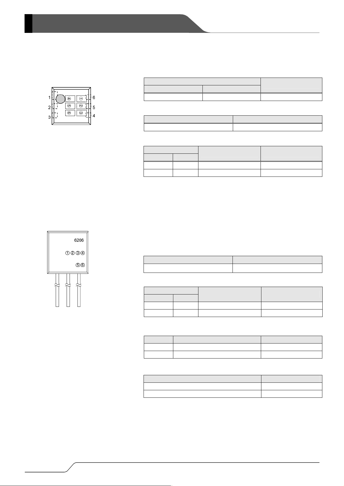
■PIN CONFIGURATION
■PIN ASSIGNMENT
PIN NUMBER
SOT-23 SOT-89 USP-6B TO-92
1
3
2
-
■PRODUCT CLASSIFICATION
●Ordering Information
XC6206P ①②③④⑤-⑥
DESIGNATOR ITEM SYMBOL DESCRIPTION
1
2
3
-
2 1 VSS Ground
4 2 VIN Power Input
6 3 VOUT Output
1, 3, 5 - NC No Connection
(*1)
*The dissipation pad for the USP-6B
package should be solder-plated in
recommended mount pattern and
metal masking so as to enhance
mounting strength and heat release.
If the pad needs to be connected to
other pins, it should be connected to
the pin number 4 (V
PIN NAME FUNCTIONS
).
IN
(SIDE VIEW)
①②
③
④⑤-⑥
The “-G” suffix denotes Halogen and Antimony free as well as being fully RoHS compliant.
2/17
Output Voltage 12~50
Accuracy
Packages
(Order Unit)
2
1
MR SOT-23 (3,000/Reel)
MR-G SOT-23 (3,000/Reel)
PR SOT-89 (1,000/Reel)
PR-G SOT-89 (1,000/Reel)
DR USP-6B (3,000/Reel)
DR-G USP-6B (3,000/Reel)
TH TO-92 (T type), Paper type (2,000/Tape)
TH-G TO-92 (T type), Paper type (2,000/Tape)
TB TO-92 (T type), Bag type (500/Bag)
TB-G TO-92 (T type), Bag type (500/Bag)
e.g. VOUT: 3.0V→①=3, ②=0
2% (V
+
+1% (VOUT≧2.0V)
≧1.5V), +30mV (VOUT<1.5V)
OUT

A
■BLOCK DIAGRAM
■
BSOLUTE MAXIMUM RATINGS
*Diodes inside the circuit are an ESD protection diode and a parasitic diode.
Ta=25OC
PARAMETER SYMBOL RATINGS UNITS
Input Voltage VIN 7.0 V
Output Current IOUT 500 * mA
Output Voltage VOUT VSS – 0.3 ~ VIN + 0.3 V
SOT-23 250
Power Dissipation
Operating Ambient Temperature Topr - 40 ~ + 85
Storage Temperature Tstg - 55 ~ + 125
* IOUT=Pd / (VIN-VOUT)
SOT-89 500
USP-6B 100
TO-92
Pd
300
mW
O
C
O
C
XC6206
Series
3/17

XC6206 Series
■ELECTRICAL CHARACTERISTICS
●XC6206P series
PARAMETER SYMBOL CONDITIONS
Output Voltage
(*4)
VOUT(E)
Maximum Output
Current
Load Regulation △VOUT
Dropout Voltage
(*5)
(*3)
I
OUTMAX - E-2 - - mA ①
V
OUT(T)>1.8V: 1mA≦IOUT≦100mA
V
OUT(T)<1.8V: 1mA≦IOUT≦50mA
IOUT=30mA
Vdif1 IOUT=30mA - E-4 mV
V
Vdif2
OUT(T)>1.8V: IOUT=100mA
V
OUT(T)<1.8V: IOUT=60mA
(*1)
MIN. TYP. MAX.
x 0.98
V
OUT(T)
(*2)
x 1.02
E-1
- - E-3 mV ①
- E-5 mV
UNIT
S
V ①
Supply Current IDD VCE=VIN - 1.0 3.0 μA ②
VOUT(T)<4.5V:VOUT(T)+1.0V≦VIN≦6.0V
V
OUT(T)>4.5V:5.5V≦VIN≦6.0V
I
OUT=30mA
- 0.05 0.25 %/V ①
Line Regulation
△V
△V
OUT
IN・VOUT
Input Voltage VIN - 1.8 - 6.0 V -
Output Voltage
Temperature
Characteristics
Short Circuit
Current
NOTE:
* 1 Unless otherwise stated, V
* 2 V
OUT(T) :Nominal voltage
OUT(E) :Effective output voltage (le. The output voltage when "VOUT(T)+1.0V" is provided at the VIN pin while maintaining a certain IOUT value.)
* 3 V
* 4 For output voltage accuracy, Please refer to E-1 table.
* 5 Vdif =V
4/17
IN
-VOUT
1
VOUT1 :A voltage equal to 98% of the output voltage whenever an amply stabilized {VOUT(T) + 1.0V} is input with each I
V
IN1 :The input voltage when VOUT1 appears as input voltage is gradually decreased.
1
△V
OUT
△Topr・V
OUT
Ishort V
IN = VOUT(T) + 1.0V
OUT
ppm/
O
C
.
IOUT=30mA
O
-40
C≦Topr≦85
IN=VOUT+1.5V, VOUT=VSS - E-6 - mA ①
O
C
- +
100 -
Ta=25OC
CIRCUIT
①
①

■ELECTRICAL CHARACTERISTICS (Continued)
●Electrical Characteristics Chart
XC6206
Series
PARAMETER
NOMINAL
VOLTAGE
1.2 1.170 1.230 460 760
1.3 1.270 1.330 400 650
1.4 1.370 1.430
1.5 1.470 1.530
1.6 1.568 1.632 250 450
1.7 1.666 1.734 200 410
1.8 1.764 1.836 150 390
1.9 1.862 1.938
2.0 1.960 2.040 1.980 2.020
2.1 2.058 2.042 2.079 2.121
2.2 2.156 2.244 2.178 2.222
2.3 2.254 2.346 2.277 2.323
2.4 2.352 2.448 2.376 2.424
2.5 2.450 2.550 2.475 2.525
2.6 2.548 2.652 2.574 2.626
2.7 2.646 2.754 2.673 2.727
2.8 2.744 2.856 2.772 2.828
2.9 2.842 2.958 2.871 2.929
3.0 2.940 3.060 2.970 3.030
3.1 3.038 3.162 3.069 3.131
3.2 3.136 3.264 3.168 3.232
3.3 3.234 3.366 3.267 3.333
3.4 3.332 3.468 3.366 3.434
3.5 3.430 3.570 3.465 3.535
3.6 3.528 3.672 3.564 3.636
3.7 3.626 3.774 3.663 3.737
3.8 3.724 3.876 3.762 3.838
3.9 3.822 3.978 3.861 3.939
4.0 3.920 4.080 3.960 4.040
4.1 4.018 4.182 4.059 4.141
4.2 4.116 4.284 4.158 4.242
4.3 4.214 4.386 4.257 4.343
4.4 4.312 4.488 4.356 4.444
4.5 4.410 4.590 4.455 4.545
4.6 4.508 4.692 4.554 4.646
4.7 4.606 4.794 4.653 4.747
4.8 4.704 4.896 4.752 4.848
4.9 4.802 4.998 4.851 4.949
5.0 4.900 5.100 4.950 5.050
OUTPUT VOLTAGE
2%
ACCURACY
VOUT(E) (V) VOUT(E) (V) IOUTMAX (mA)
MIN. MAX. MIN. MAX. MIN. MAX. TYP. MAX. TYP. MAX. TYP.
E-1 E-2 E-3 E-4 E-5 E-6
1%
ACCURACY
Not Available
MAX.
OUTPUT
CURRENT
60
80
120 50
150 55
200
250
LOAD
REGULATIO
N
UVOUT
(mV)
40
45
60
65
70
75
80 50 290 175 600
DROPOUT
VOLTAGE 1
Vdif1
(mV)
350 590
300 510
100 370
75 350 250 680
60 320 200 630
DROPOUT
VOLTAGE 2
Vdif2
(mV)
700 960
580 860
450 810
780
350
710
SHORT
CURRENT
Ishort
(mA) VOUT(T)
180
155
130
100
5/17

XC6206 Series
■TEST CIRCUITS
Circuit ①
Circuit ②
6/17

■TYPICAL PERFORMANCE CHARACTERISTICS
(1) Output Voltage vs. Output Current
(2) Current Limit
Topr=25℃ Topr=25℃
Topr=25℃
XC6206
Series
7/17
XC6206 Series
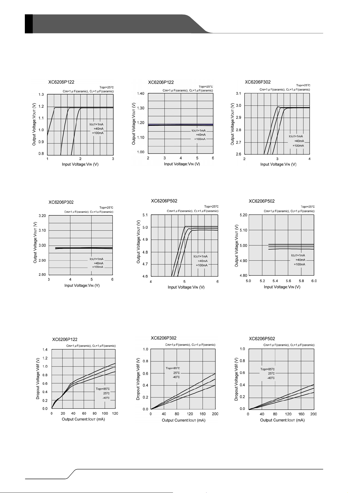
■TYPICAL PERFORMANCE CHARACTERISTICS (Continued)
(3) Output Voltage vs. Input Voltage
(4) Dropout Voltage vs. Output Current
8/17

■TYPICAL PERFORMANCE CHARACTERISTICS (Continued)
(5) Supply Current vs. Input Voltage
(6) Output Voltage vs. Ambient Temperature
XC6206
Series
9/17

XC6206 Series
■TYPICAL PERFORMANCE CHARACTERISTICS (Continued)
(7) Output Voltage vs. Ambient Temperature
(8) Input Transient Response 1
10/17
Time (0.4ms / div) Time (0.4ms / div)
Time (0.4ms / div) Time (0.4ms / div) Time (0.4ms / div)
Time (0.4ms / div)

)
■TYPICAL PERFORMANCE CHARACTERISTICS (Continued
(9) Input Transient Response 2
(10) Load Transient Response
Time (2ms / div)
Time (2ms / div) Time (2ms / div)
Time (1ms / div)
Time (2ms / div)
Time (2ms / div)
Time (2ms / div)
Time (1ms / div) Time (1ms / div)
XC6206
Series
11/17
XC6206 Series
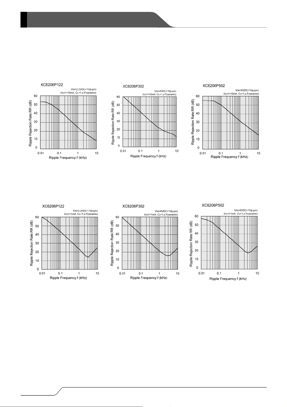
■TYPICAL PERFORMANCE CHARACTERISTICS (Continued)
(11) Ripple Rejection Rate
12/17
●
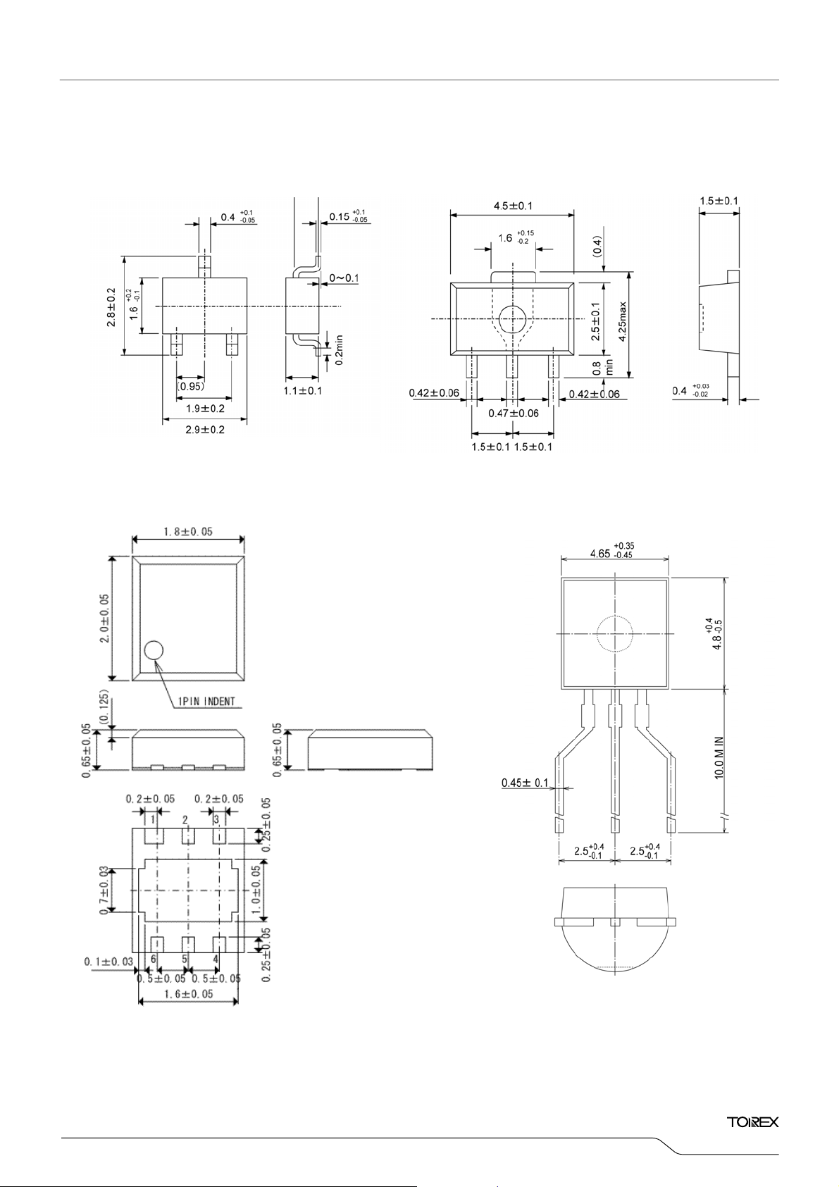
■PACKAGING INFORMATION
●SOT-23
USP-6B
Unit : mm
Unit : mm
XC6206
Series
●SOT-89
Unit : mm
●TO-92
Unit : mm
13/17
XC6206 Series
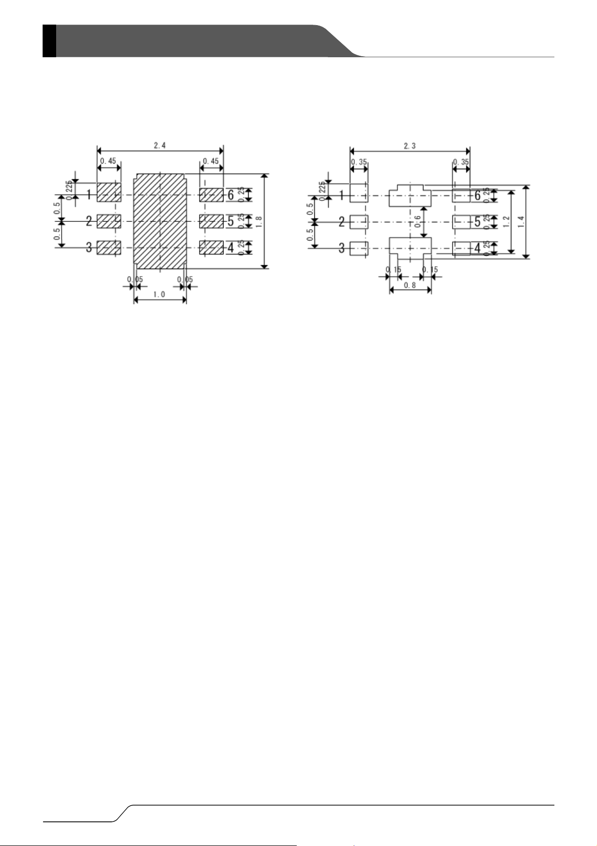
■PACKAGING INFORMATION (Continued)
●USP-6B Reference Pattern Layout ●USP-6B Reference Metal Mask Design
14/17

(
■MARKING RULE
●SOT-23, SOT-89
① represents product number
② represents 3 pins regulator
③ represents output voltage
123
④ represents producti on lot number
3
① ② ③ ④
12
SOT-23
TOP VIEW)
②①
SOT-89
(TOP VIEW)
④③
MARK PRODUCT SERIES
6 XC6206P*****
MARK
VOLTAGE=0.1 ~ 3.0V VOLTAGE=3.1 ~ 6.0V
5 6 XC6206P*****
MARK VOLTAGE (V) MARK OUTPUT VOLTAGE (V)
0 - 3.1 - F 1.6 4.6 1 - 3.2 - H 1.7 4.7 2 - 3.3 - K 1.8 4.8 3 - 3.4 - L 1.9 4.9 4 - 3.5 - M 2.0 5.0 5 - 3.6 - N 2.1 - 6 - 3.7 - P 2.2 - 7 - 3.8 - R 2.3 - 8 - 3.9 - S 2.4 - 9 - 4.0 - T 2.5 - A 4.1 - U 2.6 - -
B 1.2 4.2 - V 2.7 - C 1.3 4.3 - X 2.8 - D 1.4 4.4 - Y 2.9 - E 1.5 4.5 - Z 3.0 - -
0 to 9, A to Z, and inverted 0 to 9, A to Z repeated. (G, I, J, O, Q, W excepted.)
XC6206
Series
PRODUCT SERIES
15/17
XC6206 Series
■MARKING RULE (Continued)
●USP-6B
USP-6B
(TOP VIEW)
● TO-92
②③ represents output voltage
TO-92 (T Type)
④ represents output voltage accuracy
⑤ represents least signific ant digit of the production year
16/17
(SIDE VIEW)
①② represents product number
MARK
① ②
0 6 XC6206P***D*
③ represents 3 pins regulator
MARK PRODUCT SERIES
P XC6206P***D*
④⑤ represents output voltage
MARK
④ ⑤
OUTPUT VOLTAGE(V) PRODUCT SERIES
3 3 3.3 XC6206P33*D*
5 0 5.0 XC6206P50*D*
⑥ represents production lot number
0 to 9, A to Z repeated. (G, I, J, O, Q, W excluded)
*No character inversion used.
① represents type of regulator
MARK PRODUCT SERIES
P XC6206P*****
MARK
② ③
VOLTAGE (V) PRODUCT SERIES
3 3 3.3 XC6206P33***
5 0 5 XC6206P50***
MARK OUTPUT VOLTAGE ACCURACY PRODUCT SERIES
1
2
±1%
±2%
MARK PRODUCTION YEAR
3 2003
4 2004
⑥ represents production lot number
0 to 9, A to Z repeated. (G, I, J, O, Q, W excluded)
*No character inversion used.
PRODUCT SERIES
XC6206P**1**
XC6206P**2**

XC6206
Series
1. The products and prod uct specifications cont ained herein are subject to change without
notice to improve performance characteristics. Consult us, or our representatives
before use, to confirm that the information in this datasheet is up to date.
2. We assume no responsibility for any infringement of patents, patent rights, or other
rights arising from the use of any information and circuitry in this datasheet.
3. Please ensure suitable shipping controls (including fail-safe designs and aging
protection) are in force for equipment employing products listed in this datasheet.
4. The products in this datasheet are not developed, designed, or approved for use with
such equipment whose failure of malfunction can be reasonably expected to directly
endanger the life of, or cause significant injury to, the user.
(e.g. Atomic energy; aerospace; transport; combustion and associated safety
equipment thereof.)
5. Please use the products listed in this datasheet within the specified ranges.
Should you wish to use the products under conditions exceeding the specifications,
please consult us or our representatives.
6. We assume no responsibility for damage or loss due to abnormal use.
7. All rights reserved. No part of this datasheet may be copied or reproduced without the
prior permission of TOREX SEMICONDUCTOR LTD.
17/17
 Loading...