

XC6201 Series
ETR0301-005
Positive Voltage Regulators
■GENERAL DESCRIPTION
The XC6201 series are highly precise, low power consumption, positive voltage regulators manufactured using CMOS and
laser trimming technologies.
The series provides large currents with a significantly small dropout voltage.
The XC6201 consists of a current limiter circuit, a driver transistor, a precision reference voltage and an error amplifier. Output
voltage is selectable in 0.1V steps between 1.3V ~ 6.0V.
SOT-25, SOT-89, USP-6B and TO-92 packages are available.
■APPLICATIONS
●Mobile Phones
Cordless phones, wireless communication equipment
●
●Cameras, video recorders
●Portable games
●Portable AV equipment
●Reference voltage
●Battery powered equipment
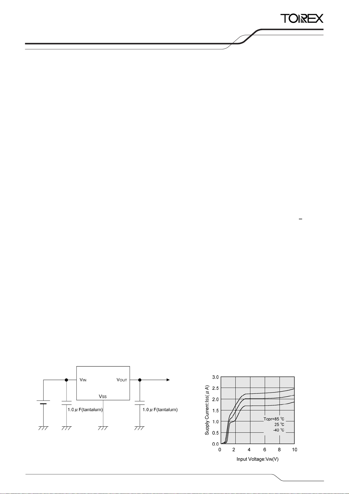
■TYPICAL APPLICATION CIRCUIT
■FEATURES
Maximum Output Current : 250mA (TYP.)
Dropout Voltage : 0.16V @ 100mA
: 0.40V @ 200mA
Maximum Operating Voltage : 10V
Output Voltage Range : 1.3V ~ 6.0V
Fixed Voltage Accuracy : ±1% (V
±2%
Low Power Consumption : 2.0μA (TYP.)
Operating Ambient Temperature
Packages : SOT-25,
Environmentally Friendly : EU RoHS Compliant, Pb Free
Tantalum or Ceramic Capacitor compatible
: -40℃ ~ 85℃
SOT-89
TO-92
USP-6B
(0.1V increments)
>2.0V)
OUT(T)
■TYPICAL PERFORMANCE
CHARACTERISTICS
●Supply Current vs. Input Voltage
XC6201P332
1/24

)
XC6201 Series
■PIN CONFIGURATION
■PIN ASSIGNMENT
(SIDE VIEW)
NC
VSS
NC
*The dissipation pad for the USP-6B
package should be solder-plated in
recommended mount pattern and
metal masking so as to enhance
mounting strength and heat release.
If the pad needs to be connected to
other pins, it should be connected to
the V
SS (No.5) pin.
VIN
NC
VOUT
PIN NUMBER
SOT-25 SOT-89/TO-92 (T) USP-6B
5 1 3 VOUT Output
2 2 5 VSS Ground
1 3 1 VIN Power Input
3, 4
■PRODUCT CLASSIFICATION
●Ordering Information
X C 6 2 0 1 P ③④⑤⑥⑦-⑧
DESIGNATOR ITEM
(*1)
The “-G” suffix denotes Halogen and Antimony free as well as being fully RoHS compliant.
* +
① ②
①
②
③④
⑤
⑥⑦-⑧
1% accuracy can be set at V
Output Voltage Accuracy
-
(*1)
Product Number 01 -
Type of Regulator P 3-pin regulator
Output Voltage
Packages
(Order Unit)
> 2.0V.
OUT(T)
2,4,6 NC No Connection
SYMBOL
13~60
1
2
MR SOT-25 (3,000/Reel)
MR-G SOT-25 (3,000/Reel)
PR SOT-89 (1,000/Reel)
PR-G SOT-89 (1,000/Reel)
TH TO-92 Taping Type: Paper type (2,000/Tape
TH-G TO-92 Taping Type: Paper type (2,000/Tape)
TB TO-92 Taping Type: Bag (500/Bag)
TB-G TO-92 Taping Type: Bag (500/Bag)
DR USP-6B (3,000/Reel)
DR-G USP-6B (3,000/Reel)
PIN NAME FUNCTION
e.g. 30:3.0V
50:5.0V
±1%
±2%
DESCRIPTION
2/24
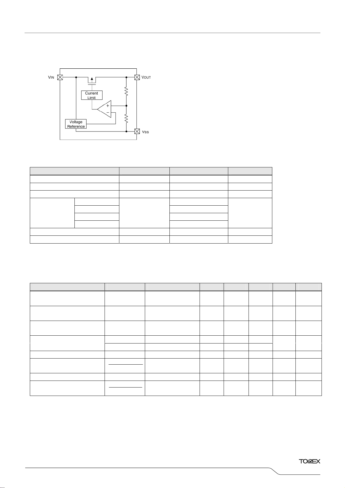
■BLOCK DIAGRAM
■ABSOLUTE MAXIMUM RATINGS
PAR AMETER SYMBOL RATINGS UNITS
Input Voltage VIN 12.0 V
Output Current IOUT 500 mA
Output Voltage VOUT
SOT-25 250
Power
Dissipation
SOT-89 500
TO-92 300
Pd
USP-6B
Operating Temperature Topr
Storage Temperature Tstg
■ELECTRICAL CHARACTERISTICS
XC6201P132
VOUT(T)=1.3V
(*1)
PAR AMETER SYMBOL CONDITIONS MIN. TYP. MAX. UNITS
Output Voltage
V
OUT(E)
Maximum Output Current IOUTmax
Load Regulation
Dropout Voltage
(*3)
OUT
△V
Vdif1 IOUT=30mA - 200 600
Vdif2 I
(*2)
V
I
OUT=10mA
V
OUT(E)≧1.17V
V
V
1mA≦IOUT≦30mA
OUT=60mA - 500 810
Supply Current ISS VIN=2.3V - 2.0 5.0
Line Regulation
OUT
△V
△VIN・△VOUT
IOUT=10mA
2.3V≦VIN≦10.0V
Input Voltage VIN 1.8 - 10 V -
Output Voltage
Temperature Characteristics
△VOUT
△Topr・△VOUT
IOUT=40mA
-40℃≦Topr≦85℃
SS-0.3~VIN+0.3
V
IN=2.3V
IN=2.3V
IN=2.3V
V
mW
120
-40~+85 ℃
-55~+125 ℃
1.274 1.300 1.326 V
60 - - mA
- 10 30 mV
- 0.2 0.3
-
±100
Ta = 2 5 ℃
-
XC6201
Series
Ta =2 5℃
CIRCUIT
②
②
②
mV
μA ①
%/V ②
ppm/℃ ②
②
3/24
XC6201 Series
■ELECTRICAL CHARACTERISTICS (Continued)
XC6201P182
VOUT(T)=1.8V
PAR AMETER SYMBOL CONDITIONS MIN. TYP. MAX. UNITS
Output Voltage
Maximum Output Current IOUTmax
Load Regulation
Dropout Voltage
(*3)
Supply Current ISS VIN=2.8V - 2.0 5.0
Line Regulation
Input Voltage VIN 1.8 - 10 V -
Output Voltage
Temperature Characteristics
XC6201P272
VOUT(T)=2.7V
PAR AMETER SYMBOL CONDITIONS MIN. TYP. MAX. UNITS
Output Voltage
Maximum Output Current IOUTmax
Load Regulation
Dropout Voltage
(*3)
Supply Current ISS VIN=3.7V - 2.0 5.0
Line Regulation
Input Voltage VIN 1.8 - 10 V -
Output Voltage
Temperature Characteristics
(*1)
OUT(E)
V
△V
OUT
(*2)
VIN=2.8V
I
OUT=40mA
VIN=2.8V
VOUT(E)≧1.62V
V
IN=2.8V
≦
IOUT≦40mA
1mA
1.764 1.800 1.836 V
80 - - mA
Vdif1 IOUT=40mA - 200 370
Vdif2 I
OUT
△V
△V
IN・△VOUT
△V
OUT
△Topr・△V
(*1)
(*2)
OUT(E)
V
OUT
△V
OUT
OUT=80mA - 450 710
IOUT=40mA
2.8V≦VIN≦10.0V
IOUT=40mA
-40℃≦Topr≦85℃
VIN=3.7V
I
OUT=40mA
VIN=3.7V
VOUT(E)≧2.43V
V
IN=3.7V
2.646 2.700 2.754 V
100 - - mA
1mA≦IOUT≦60mA
Vdif1 IOUT=60mA - 200 370
Vdif2 I
OUT
△V
△V
IN・△VOUT
△V
OUT
△Topr・△V
OUT
OUT=120mA - 450 710
IOUT=40mA
3.7V≦VIN≦10.0V
IOUT=40mA
-40℃≦Topr≦85℃
Ta =2 5℃
CIRCUIT
- 10 30 mV
mV
μA ①
- 0.2 0.3 %/V
-
±100
-
ppm/℃ ②
Ta =2 5℃
CIRCUIT
- 15 40 mV
mV
μA ①
- 0.2 0.3
-
±100
-
%/V ②
ppm/℃ ②
②
②
②
②
②
②
②
②
②
4/24

■ELECTRICAL CHARACTERISTICS (Continued)
XC6201P332
VOUT(T)=3.3V
(*1)
PAR AMETER SYMBOL CONDITIONS MIN. TYP. MAX. UNITS
Output Voltage
V
OUT(E)
Maximum Output Current IOUTmax
Load Regulation
Dropout Voltage
(*3)
OUT
△V
Vdif1 IOUT=80mA - 200 360
Vdif2 I
(*2)
VIN=4.3V
I
OUT=40mA
VIN=4.3V
VOUT(E)≧2.97V
V
IN=4.3V
1mA≦IOUT≦80mA
OUT=160mA - 450 700
3.234 3.300 3.366 V
150 - - mA
- 20 50 mV
Supply Current ISS VIN=4.3V - 2.0 5.0
Line Regulation
△V
△V
IN・△VOUT
OUT
IOUT=40mA
4.3V≦VIN≦10.0V
- 0.2 0.3
Input Voltage VIN 1.8 - 10 V -
Output Voltage
Temperature Characteristics
XC6201P502
△Topr・△V
VOUT(T)=5.0V
(*1)
△V
OUT
OUT
IOUT=40mA
-40℃≦Topr≦85℃
-
PAR AMETER SYMBOL CONDITIONS MIN. TYP. MAX. UNITS
Output Voltage
V
OUT(E)
Maximum Output Current IOUTmax
Load Regulation
Dropout Voltage
(*3)
OUT
△V
Vdif1 IOUT=100mA - 160 340
Vdif2 IOUT=200mA - 400 600
(*2)
VIN=6.0V
I
OUT=40mA
VIN=6.0V
VOUT(E)≧4.57V
V
IN=6.0V
1mA≦IOUT≦100mA
4.900 5.000 5.100 V
200 - - mA
- 30 70 mV
Supply Current ISS VIN=6.0V - 2.0 6.0
OUT=40mA
Line Regulation
△V
△V
IN・△VOUT
OUT
6.0V
I
≦
VIN≦10.0V
- 0.2 0.3
Input Voltage VIN 1.8 - 10 V -
Output Voltage
Temperature Characteristics
NOTE:
OUT(T) = Nominal output voltage.
*1: V
OUT(E) = Effective output voltage (i.e. the output voltage when “VOUT(T)+1.0V” is provided while
*2: V
maintaining a certain I
*3: Vdif = (V
V
V
IN1- VOUT1)
IN1 :An Input Voltage when VOUT1 appears as the input voltage is gradually decreased.
OUT1 : A voltage equal to 98% of the output voltage when a stabilized (VOUT(T) + 1.0V) is input.
△Topr・△V
OUT value).
△V
OUT
OUT
I
OUT=40mA
-40℃
≦
Topr≦85℃
-
±100
±100
-
ppm/℃ ②
-
ppm/℃ ②
XC6201
Series
Ta =2 5℃
CIRCUIT
②
②
②
mV
μA ①
%/V ②
mV
μA ①
%/V ②
②
Ta =2 5℃
CIRCUIT
②
②
②
②
5/24
XC6201 Series
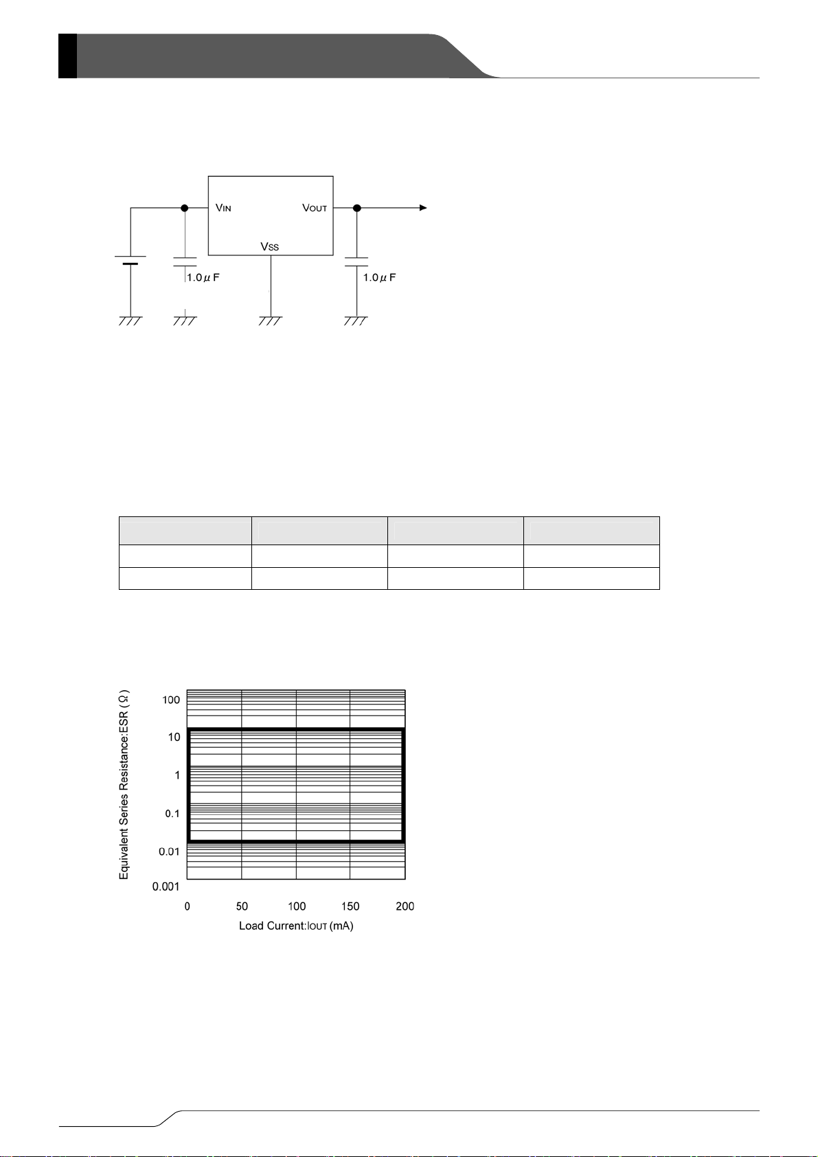
■TYPICAL APPLICATION CIRCUIT
With the XC6201 series regulator, in order to ensure the stabilized output voltage, we suggest that an output capacitor (CL) of
1μF or more be connected between the output pin (V
capacitors), please make sure that the output voltage is more than 1.7V. When the output voltage is from 1.3V to 1.6V, the
output capacitor should be a tantalum capacitor with a capacitance of 2.2μF. We also suggest an input capacitor (C
should be connected between the VIN and the VSS in order to stabilize input power source.
OUTPUT VOLTAGE CIN CL (TANTALUM) CL (LOW ESR)
(Tantalum)
1.3V~1.6V ≧1.0μF ≧2.2μF -
1.7V~6.0V ≧1.0μF ≧1.0μF ≧1.0μF
VIN=1.8V~10V,V
=1.0μF(Ceramic),C
C
(Tantalum)
OUT) and the VSS pin. For using low ESR capacitor (e.g. ceramic
=1.7~6.0V
OUT
=1.0μF(ceramic)
IN)
6/24
XC6201
Series
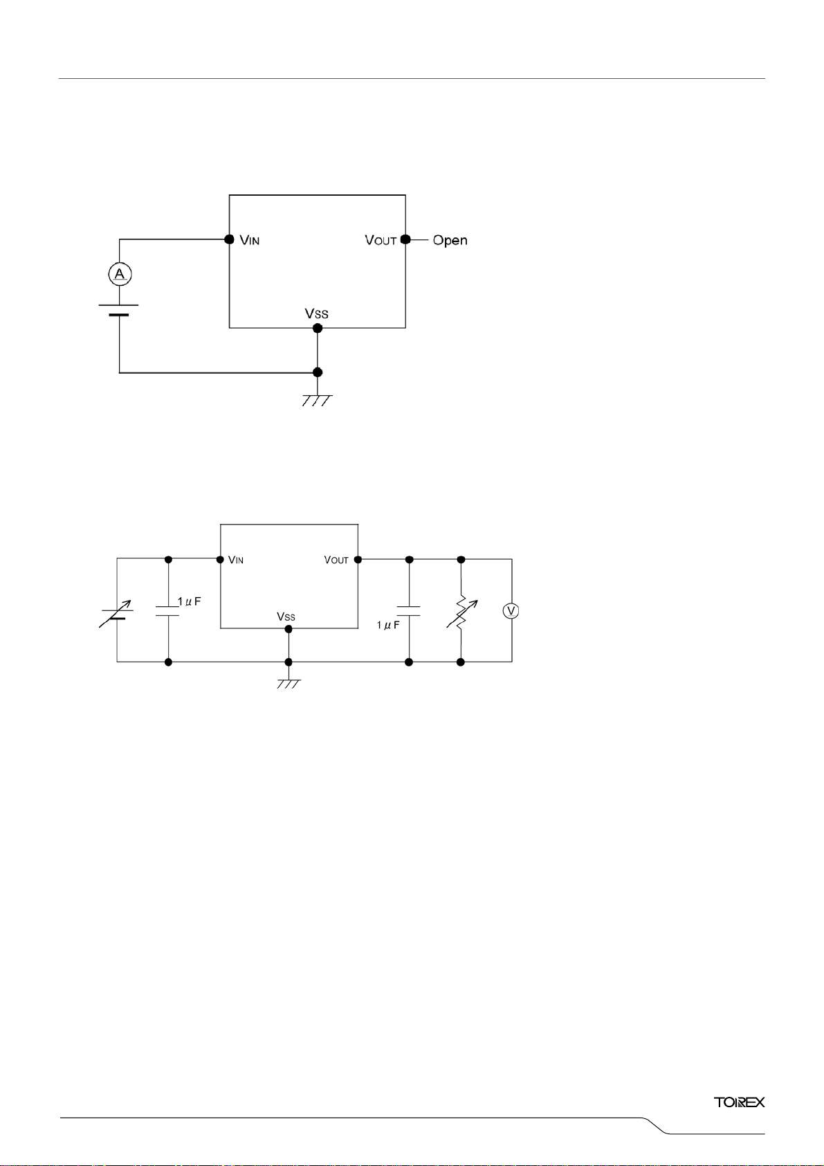
■TEST CIRCUITS
Circuit ① : Supply Current
Circuit ② : Output Voltage, Oscillation, Line Regulation, Dropout Voltage, Load Regulation
■ NOTE ON USE
1. Please use this IC within the stated absolute maximum ratings. The IC is liable to malfunction should the ratings be
exceeded. When a voltage higher than the V
Schottky barrier diode between the V
OUT and the VIN and do not exceed the VOUT rating.
2. An oscillation may occur by the impedance between a power supply and the input of the IC. Where the impedance is 10Ω
or more, please use an input capacitor (C
increasing the input capacitor value. Also an oscillation may occur if the input capacitor value is smaller than the input
impedance when the output capacitance (C
input capacitor value or reducing the output capacitor value.
3. Please ensure that output current (I
OUT) is less than Pd / (VIN - VOUT) and do not exceed the rated power dissipation value
(Pd) of the package.
IN flows to the VOUT like when using two power supplies, please connect a
IN) of at least 1μF. In case of high output current, operation can be stabilized by
L) is large. In such cases, operations can be stabilized by either increasing the
7/24
XC6201 Series
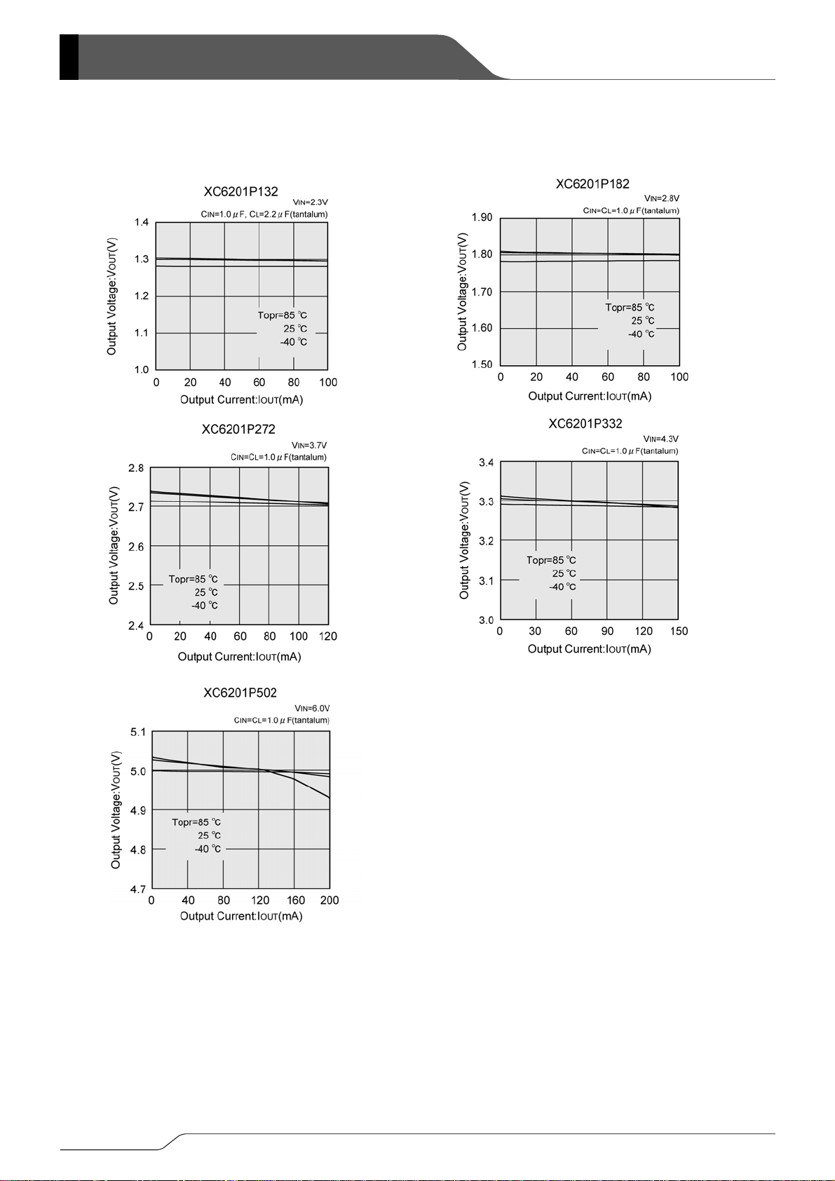
■TYPICAL PERFORMANCE CHARACTERISTICS
(1) Output Voltage vs. Output Current
8/24

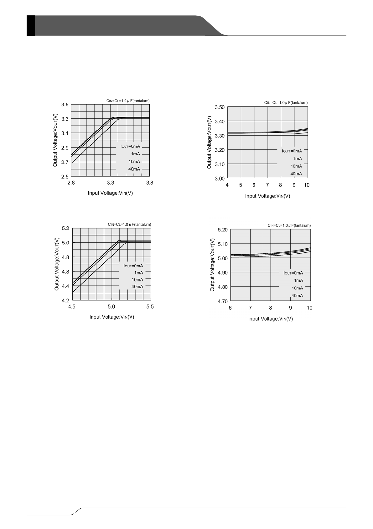
■TYPICAL PERFORMANCE CHARACTERISTICS (Continued)
(2) Output Voltage vs. Input Voltage
XC6201P132
XC6201P182
XC6201P272
XC6201P132
XC6201P182
XC6201P272
XC6201
Series
9/24
XC6201 Series
■TYPICAL PERFORMANCE CHARACTERISTICS (Continued)
(2) Output Voltage vs. Input Voltage (Continued)
XC6201P332
XC6201P332
XC6201P502 XC6201P502
10/24

■TYPICAL PERFORMANCE CHARACTERISTICS (Continued)
(3) Dropout Voltage vs. Output Current
XC6201P132 XC6201P182
XC6201P272 XC6201P332
XC6201P502
XC6201
Series
11/24

XC6201 Series
■TYPICAL PERFORMANCE CHARACTERISTICS (Continued)
(4) Supply Current vs. Input Voltage
XC6201P132 XC6201P132
XC6201P182
12/24

■TYPICAL PERFORMANCE CHARACTERISTICS (Continued)
(4) Supply Current vs. Input Voltage (Continued)
XC6201P332
XC6201
Series
13/24
XC6201 Series
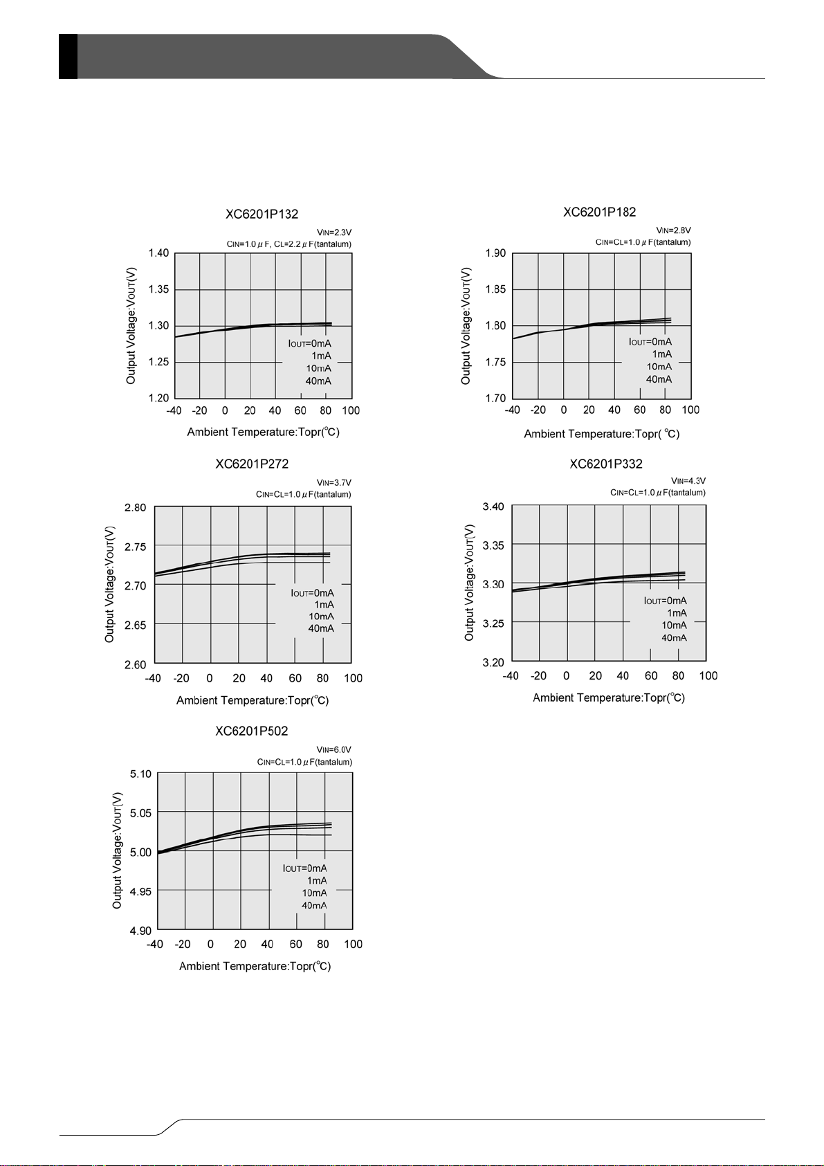
■TYPICAL PERFORMANCE CHARACTERISTICS (Continued)
(5) Output Voltage vs. Ambient Temperature
14/24
■TYPICAL PERFORMANCE CHARACTERISTICS (Continued)
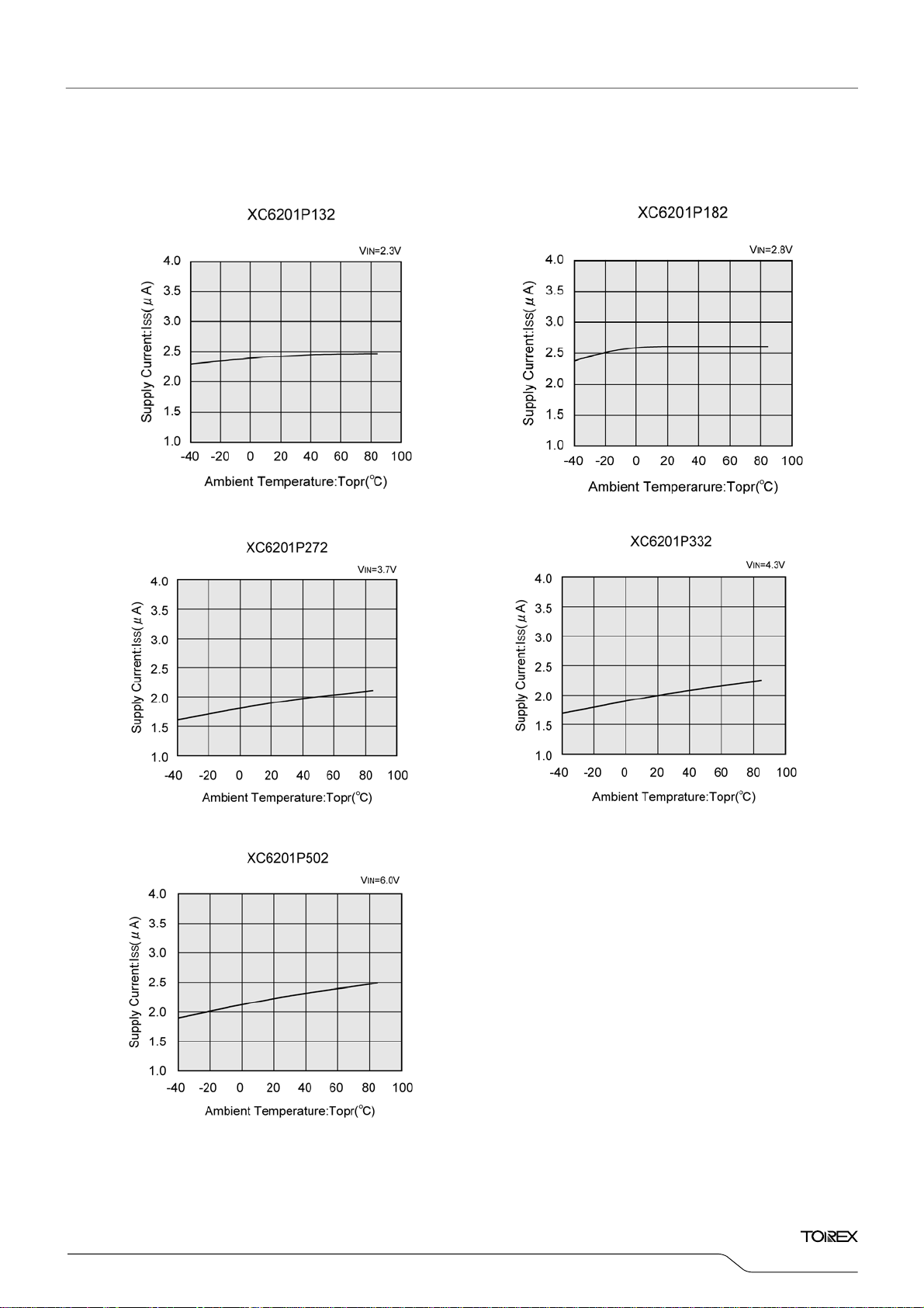
(6) Supply Current vs. Ambient Temperature
XC6201
Series
15/24

XC6201 Series
■TYPICAL PERFORMANCE CHARACTERISTICS (Continued)
(7) Input Transient Response
XC6201P132 XC6201P182
Time (1ms/div) Time (1ms/div)
XC6201P272 XC6201P332
Time (1ms/div) Time (1ms/div)
XC6201P502
Time (1ms/div)
16/24

■TYPICAL PERFORMANCE CHARACTERISTICS (Continued)
(8) Load Transient Response
XC6201P132
Time (2ms/div) Time (2ms/div)
XC6201P272 XC6201P332
Time (2ms/div) Time (2ms/div)
XC6201P502
Time (2ms/div)
XC6201P182
XC6201
Series
17/24

XC6201 Series
■TYPICAL PERFORMANCE CHARACTERISTICS (Continued)
(9) Ripple Rejection Rate
(10) Output Noise Density
XC6201P132 XC6201P182
XC6201P272
XC6201P332
XC6201P502
XC6201P302
18/24

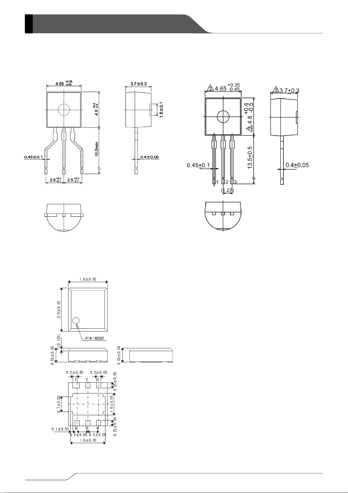
■PACKAGING INFORMATION
●SOT-25
+0.1
0.4
-0.05
2.9±0.2
5 4
+0.2
-0.1
1.6
2.8±0.2
1
2
(0.95)
1.9±0.2
3
1.3MAX
1.1±0.1
●SOT-89
0.15
+0.1
-0.05
XC6201
Series
Unit : mm
0~0.1
0.2MIN
Unit : mm
19/24
XC6201 Series
■PACKAGING INFORMATION (Continued)
●TO-92
Paper type Bag
●USP-6B
Unit : mm
Unit : mm
Unit : mm
20/24

■PACKAGING INFORMATION (Continued)
XC6201
Series
●USP-6B Reference Pattern Layout
●USP-6B Reference Metal Mask Design
21/24

(
(
XC6201 Series
■MARKING RULE
●SOT-89, SOT-25
②①
123
SOT-89
TOP VIEW)
54
① ② ③ ④
123
SOT-25
TOP VIEW)
④③
① represents the product series
MARK PRODUCT SERIES
1 XC6201xxxxxx
② represents type of regulator
MARK
Voltage= 0.1 ~ 3.0V Voltage= 3.1 ~ 6.0V
PRODUCT SERIES
5 6 XC6201PXXXXX
8 9 XC6201TXXXPX
③ represents output voltage
MARK OUTPUT VOLTAGE (V) MARK OUTPUT VOLTAGE (V)
0
1
2
3
4
5
6
7
8
9
A
B
-
-
-
-
-
-
-
-
-
-
-
-
C 1.3 4.3
D 1.4 4.4
E 1.5 4.5
3.1
3.2
3.3
3.4
3.5
3.6
3.7
3.8
3.9
4.0
4.1
4.2
-
-
-
-
-
-
-
-
-
-
-
-
-
-
-
F 1.6 4.6
H 1.7 4.7
K 1.8 4.8
L 1.9 4.9
M 2.0 5.0
N 2.1 5.1
P 2.2 5.2
R 2.3 5.3
S 2.4 5.4
T 2.5 5.5
U 2.6 5.6
V 2.7 5.7
X 2.8 5.8
Y 2.9 5.9
Z 3.0 6.0
④ represents assembly lot number
0 to 9, A to Z repeated (G, I, J, O, Q, W excluded)
-
-
-
-
-
-
-
-
-
-
-
-
-
-
-
22/24

■MARKING RULE (Continued)
●TO-92
(SIDE VIEW)
① represents type of regulator
MARK PRODUCT SERIES
P XC6201Pxxxxx
T XC6201Txxxxx
②③ represents output voltage
② ③
3 3 3.3 XC6201Px33xx
5 0 5.0 XC6201Px50xx
④ represents detect voltage accuracy
MARK DETECT VOLTAGE ACCURACY PRODUCT SERIES
●USP-6B
USP-6B
(TOP VIEW)
⑤ represents least significant digit of production year
MARK PRODUCTION YEAR
⑥ represents the production lot number
0 to 9, A to Z repeated (G, I, J, O, Q, W excluded)
Note: No character inversion used.
①② represents product series
③ represents type of regulator
MARK TYPE PRODUCT SERIES
④⑤ represents output voltage
④ ⑤
3 3 3.3 XC6201x33xDx
5 0 5.0 XC6201x50xDx
XC6201
Series
MARK
1
2
3 2003
4 2004
MARK
① ②
0 1 XC6201xxxxDx
P 3pin Regulator XC6201PxxxDx
T VIN=7V(Rated)
MARK
VOLTAGE (V) PRODUCT SERIES
Within ±1%
Within ±2%
XC6201Pxx1xx
XC6201Pxx2xx
PRODUCT SERIES
XC6201TxxxDx
VOLTAGE (V) PRODUCT SERIES
⑥ represents assembly lot number
0 to 9, A to Z repeated (G, I, J, O, Q, W excluded)
Note: No character inversion used.
23/24

XC6201 Series
1. The products and product specifications contained herein are subject to change without
notice to improve performance characteristics. Consult us, or our representatives
before use, to confirm that the information in this datasheet is up to date.
2. We assume no responsibility for any infringement of patents, patent rights, or other
rights arising from the use of any information and circuitry in this datasheet.
3. Please ensure suitable shipping controls (including fail-safe designs and aging
protection) are in force for equipment employing products listed in this datasheet.
4. The products in this datasheet are not developed, designed, or approved for use with
such equipment whose failure of malfunction can be reasonably expected to directly
endanger the life of, or cause significant injury to, the user.
(e.g. Atomic energy; aerospace; transport; combustion and associated safety
equipment thereof.)
5. Please use the products listed in this datasheet within the specified ranges.
Should you wish to use the products under conditions exceeding the specifications,
please consult us or our representatives.
6. We assume no responsibility for damage or loss due to abnormal use.
7. All rights reserved. No part of this datasheet may be copied or reproduced without the
prior permission of TOREX SEMICONDUCTOR LTD.
24/24
 Loading...