

■
■
■
XC61H Series
ETR0212-004
Voltage Detector with Delay Circuit Built-In
GENERAL DESCRIPTION
The XC61H series is a highly accurate, low power consumption CMOS voltage detector with a delay circuit. Detect voltage is
accurate with minimal temperature drift. Output configurations are available in both CMOS and N-channel open drain.
Since the full delay circuit is built-in, an external delay-time capacitor is not necessary so that high density mounting is possible.
■APPLICATIONS
●Microprocessor reset circuitry
●System battery life and charge voltage monitors
●Memory battery back-up circuits
●Power-on reset circuits
●Power failure detection
●
Delay circuitry
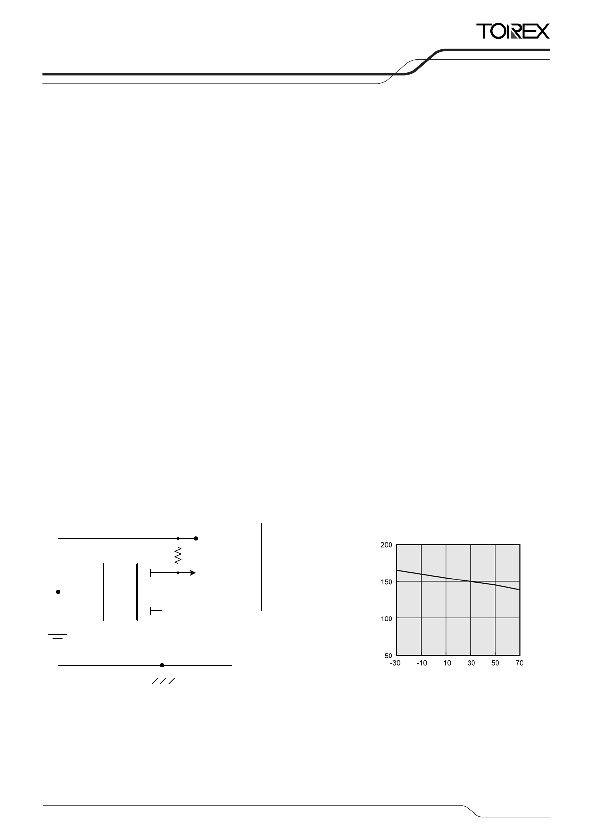
TYPICAL APPLICATION CIRCUITS
VIN
3
XC61HN series
R pull
RESETB
2
V
SS
1
Rpull is not necessary with CMOS output products
μP
IN
V
RESETB
INPUT
VSS
Not necessary with CMOS output products
■FEATURES
Detect Voltage Accuracy : ± 2%
Low Power Consumption
Detect Voltage Range
Operating Voltage Range
: 1.0μA(TYP.)[ V
:
1.6V ~ 6.0V (0.1V increments)
: 0.7V ~ 10.0V
Detect Voltage Temperature Characteristics
: ±100ppm/℃(TYP.)
Built-In Release Delay time : 1ms (MIN.)
50ms (MIN.)
80ms (MIN.)
N-ch
Output Configuration :
Operating Ambient T emperat ure
Package :
open drain output or CMOS
:
30℃〜+80℃
SOT-23
Environmentally Friendly : EU RoHS Compliant, Pb Free
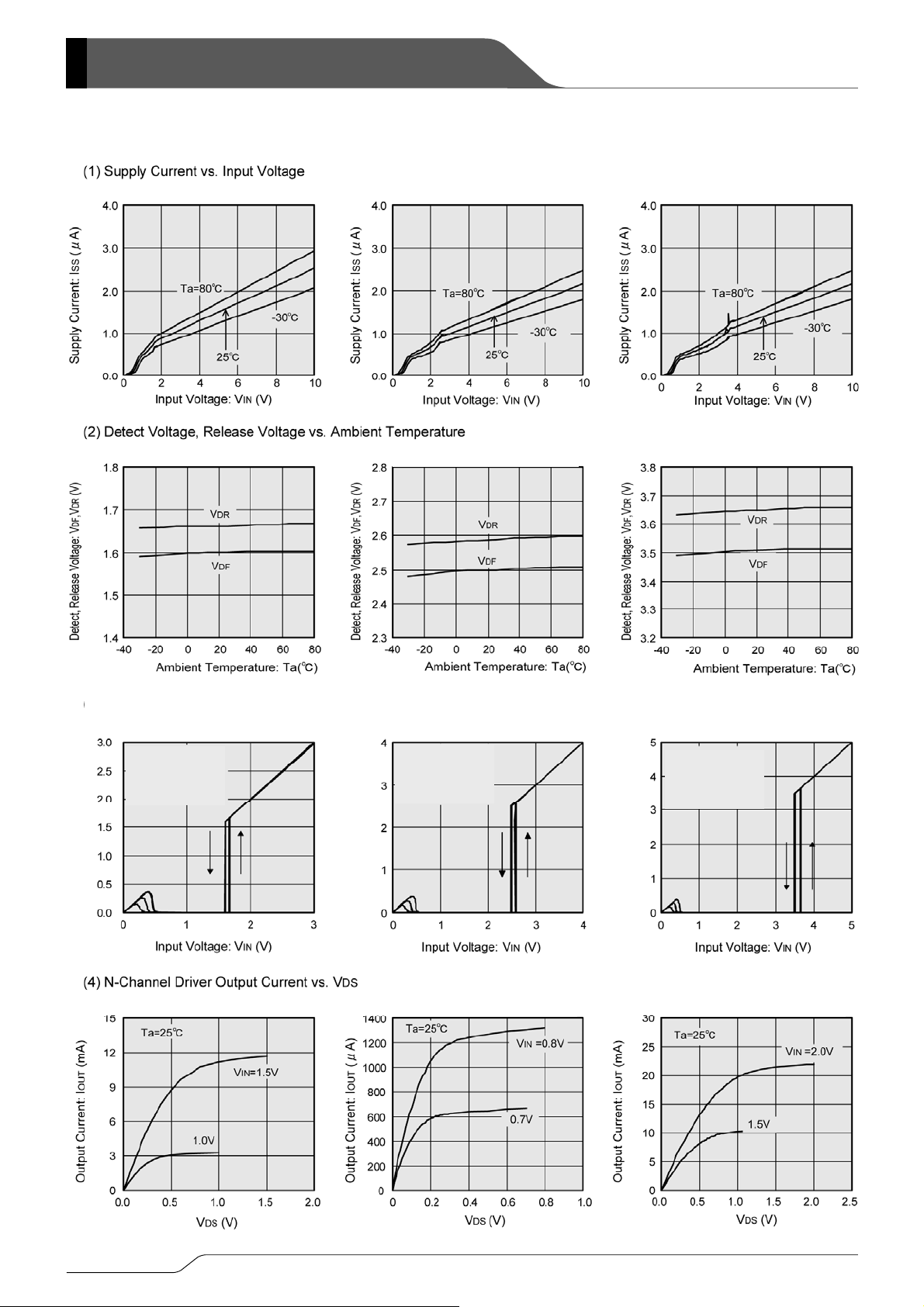
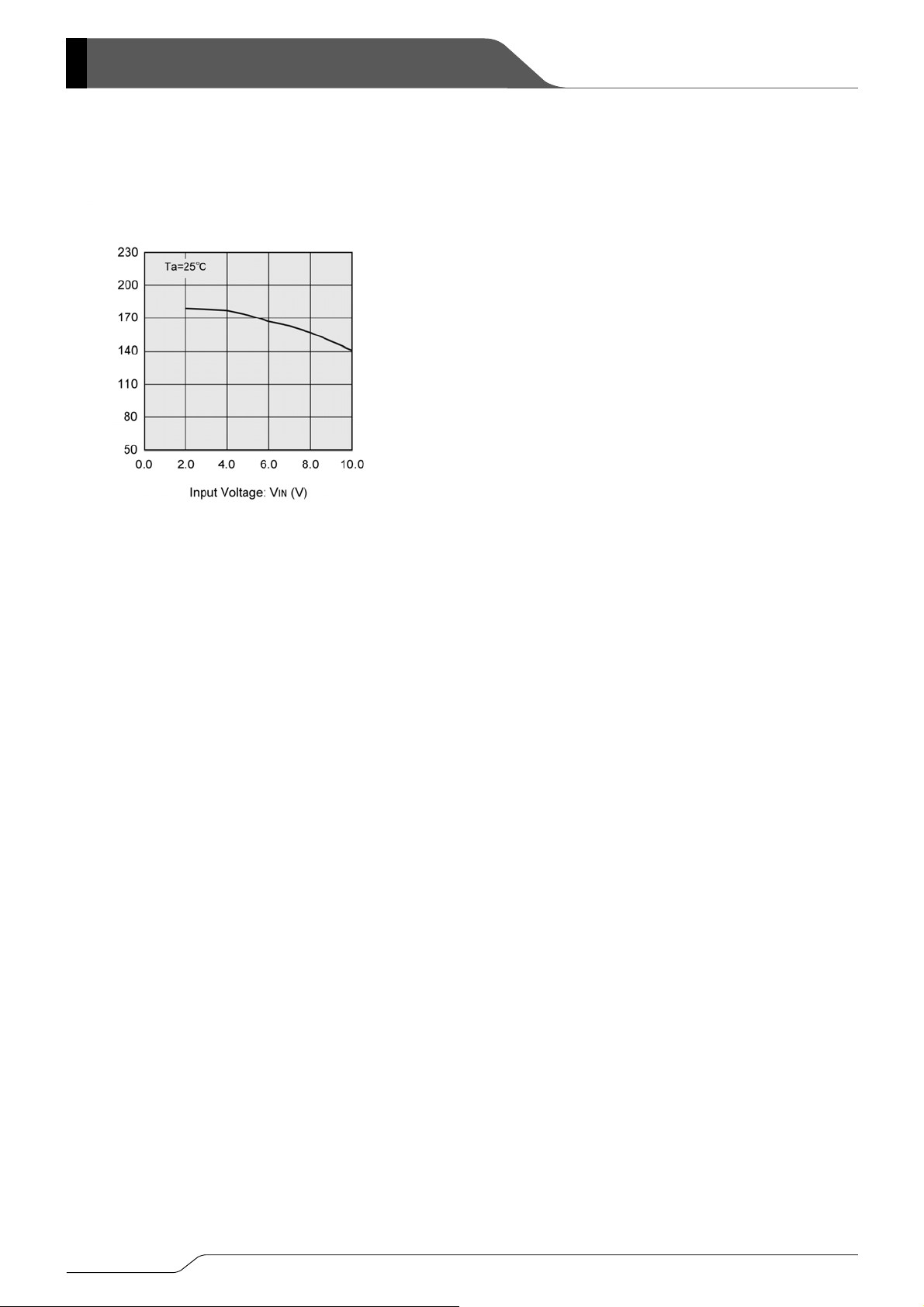
TYPICAL PERFORMANCE
CHARACTERISTICS
●Release Delay Time (tDR) vs. Ambient Temperature
XC61HC3012
(ms)
DR
Release Delay Time: t
Ambient Temperature: Ta (℃)
=2.0V ]
IN
1/13

■
■
■
■
XC61H Series
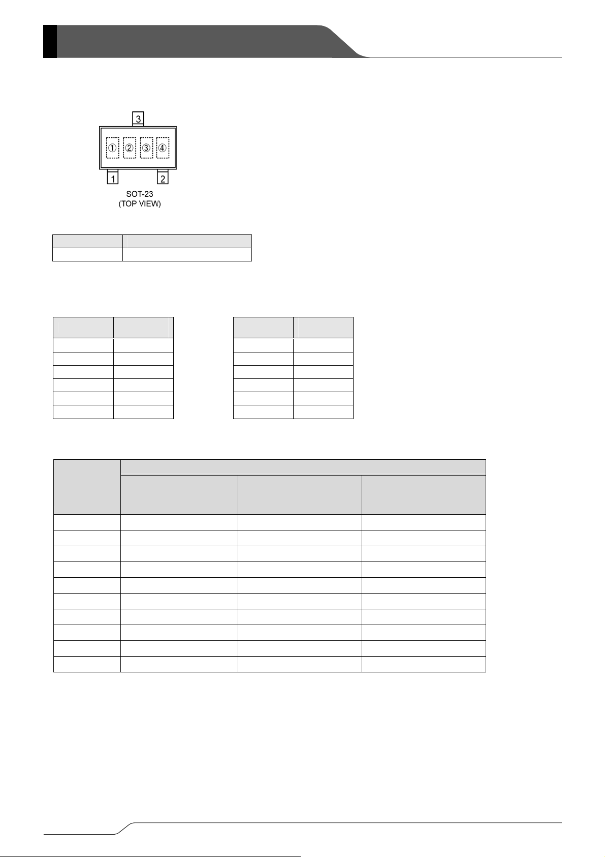
PIN CONFIGURATION
(TOP VIEW)
PRODUCT CLASSIFICATION
●Ordering Information
XC61H①②③④⑤⑥⑦-⑧
DESIGNATOR ITEM SYMBOL DESCRIPTION
①
②③
④
⑤
⑥⑦-⑧
(*1) The ”-G” suffix indicates that the products are Halogen and Antimony free as well as being fully RoHS compliant.
(*2) No parts are available with an accuracy of ± 1%
BLOCK DIAGRAMS
(1)CMOS output
(*1)
(*1)
Output Configuration
Detect Voltage (V
Release Delay Time
Detect Accuracy 2
Package
(Oder Unit)
) 16 ~ 60
DF
C CMOS output
N N-ch open drain output
1 50ms ~ 200ms
4 80ms ~ 400ms
5 1ms ~ 50ms
MR-G SOT-23 (3000/Reel)
PIN ASSIGNMENT
PIN NUMBER
SOT-23
1 VSS Ground
2
3 VIN Supply Voltage Input
e.g. 2.5V → ②2 , ③5
± 2.0%
(*2)
(2)N-ch open drain output
PIN NAME FUNCTION
RESETB
Output
2/13
■
A
■
BSOLUTE MAXIMUM RATINGS
PAR AMETER SYMBOL RATINGS UNITS
Input Voltage VIN V
Output Current I
Output Voltage
Power Dissipation
N-ch open drain output
SOT-23 Pd 250 mW
CMOS
Operating Ambient Temperature Topr
Storage Temperature Tstg
ELECTRICAL CHARACTERISTICS
PAR AMETER
Detect Voltage
Hysteresis Width
Supply Current
(*1)
Operating Voltage
Output Current I
SYMBOL
V
DF
V
HYS
ISS
V
IN
OUT
OUT
V
RESETB
V
V
V
=1.6V〜6.0V
V
DF
V
V
N-ch, VDS = 0.5V VIN = 3.0V 5.0 10.1 -
V
V
P-ch, V
(CMOS Output)
Ta =2 5℃
-0.3 ~ 12.0 V
SS
50 mA
VSS-0.3 ~VIN+0.3
VSS -0.3 ~ 12
V
-30〜+80 ℃
-40〜+125 ℃
CONDITIONS MIN. TYP. MAX.
= 1.5V
IN
= 2.0V
IN
= 3.0V
IN
V
= 4.0V
IN
VIN = 5.0V
V
DF(T)
x 0.98
VDF
x 0.02
V
DF(T)
V
x 0.05
- 0.9 2.6
- 1.0 3.0
- 1.3 3.4
- 1.6 3.8
- 2.0 4.2
DF
V
x 1.02
VDF
x 0.08
0.7 - 10.0 V
=2.1V
DS
= 1.0V
IN
= 2.0V 3.0 7.7 -
IN
= 4.0V 6.0 11.5 -
IN
= 5.0V 7.0 13.0 -
IN
VIN = 8.0V
1.0
-10.0 -2.0
2.2
DF(T)
-
UNITS
μA ②
mA
V
V
XC61H
Series
Ta = 2 5 ℃
CIRCUIT
①
①
①
③
④
CMOS Output
Leakage
Current
(Pch)
Nch Open
I
LEAK
Drain Output
Δ
Detect Voltage
Temperature Characteristics
Release Delay Time
DR → RESETB inversion)
(V
VDF (T) is nominal detect voltage value
Release Voltage: V
(*1) The supply current during power-start until output being stable (during release operation) is 2μA greater with comparison to the period
after the completion of release operation because of the shoot-through current in delay current.
DR = VDF + VHYS
VDF/
(
Δ
Topr・VDF)
tDR VIN changes from 0.6V to 10V
V
IN=VDF
x 0.9V, V
=0V - -0.01 -
RESETB
μA ③
V
=10.0V, V
IN
-30℃≦Topr≦80℃
=10.0V - 0.01 0.1
RESETB
- ±100 -
ppm/℃
50 - 200
80 - 400
ms
1 - 50
①
⑤
3/13

■
XC61H Series
OPERATIONAL EXPLANATION
●CMOS output
① An input voltage V
higher than detect voltage V
*Note that high impedance exists at RESETB with the N-channel open drain output configuration. If the RESETB pin is
pulled up, RESETB will be equal to the pull up voltage.
② When VIN falls below VDF, RESETB will be equal to ground voltage VSS level (detect state).
* Note that this also applies to N-channel open drain output configurations.
③ When VI
N falls to a level below that of the minimum operating voltage VMIN, output will become unstable.
*When the output pin is generally pulled up with N-channel open drain output configurations, output will be equal to pull
up voltage.
④ When V
IN rises above the VSS level (excepting levels lower than minimum operating voltage), RESETB will be equal to
VSS until VIN reaches the VDR level.
⑤ Although V
IN will rise to a level higher than VDR, RESETB maintains ground voltage level via the delay circuit.
⑥ After taking a release delay time, V
*High impedance exists with the N-channel open drain output configuration and that voltage will be dependent on pull up.
Notes:
1. The difference between V
2. Release delay time (tDR) represents the time it takes until when VIN voltage appears at RESETB pin once the input
voltage has exceeded the V
●Timing Chart
starts higher than the release voltage VDR. Then, VIN voltage will gradually fall. When VIN voltage is
IN
DF, output voltage RESETB is equal to the VIN voltage.
IN voltage will be output at the RESETB pin.
DR and VDF represents the hysteresis width.
DR level.
4/13
Output Voltage (RESETB)
Release Delay Time (tDR)

XC61H
■NOTES ON USE
1. Please use this IC within the stated maximum ratings. For temporary, transitional voltage drop or voltage rising
phenomenon, the IC is liable to malfunction should the ratings be exceeded.
2. When a resistor is connected between the V
oscillation may occur as a result of voltage drops at R
resistor be added. (refer to Figure 1 below)
3. When a resistor (RIN) is connected between the VIN pin and the power supply with CMOS output configurations,
irrespective of N-ch open drain output configurations, oscillation may occur as a result of shoot-through current at the time
of voltage release even if load current (I
4. If a resistor (RIN) must be used, then please use with as small a level of input impedance as possible in order to control the
occurrences of oscillation as described above. Further, please ensure that R
0.1μF, please test with the actual device. However, N-ch open drain output only. (Figure 1).
5. With a resistor RIN connected between the V
power supply voltage as a result of the IC's supply current flowing through the V
6. Depending on circuit's operation, release delay time of this IC can be widely changed due to upper limits or lower limits of
operational ambient temperature.
7. Torex places an importance on improving our products and its reliability.
However, by any possibility, we would request user fail-safe design and post-aging treatment on system or equipment.
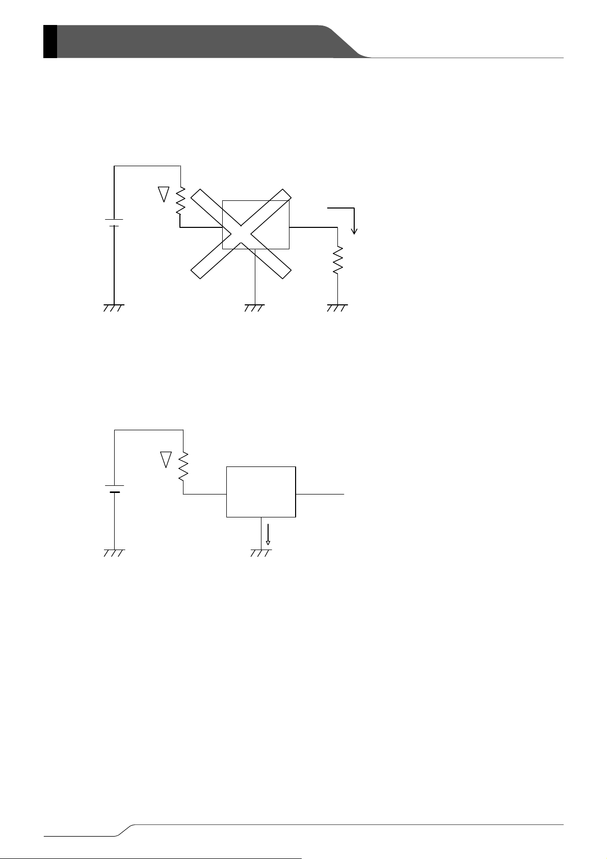
●Irregular Oscillations
(1) Irregular oscillation as a result of load current with the CMOS output configuration:
When the voltage applied at power supply, release operations commence and the detector's output voltage
increases. Load current (I
located between the power supply and the VIN pin, the load current will flow via the IC's VIN pin. The voltage drop will
also lead to a fall in the voltage level at the VIN pin. When the VIN pin voltage level falls below the detect voltage level,
detect operations will commence. Following detect operations, load current flow will cease and since voltage drop at
R
will disappear, the voltage level at the VIN pin will rise and release operations will begin over again.
IN
Irregular oscillation may occur with this "release - detect - release" repetition.
Further, this condition will also appear via means of a similar mechanism during detect operations.
(2) Irregular oscillation as a result of shoot-through current:
Since the XC61H series are CMOS IC
operates (during release and detect operations). Consequently, irregular oscillation is liable to occur during release
voltage operations as a result of output current which is influenced by this shoot-through current (Figure 3).
Since hysteresis exists during detect operations, irregular oscillation is unlikely to occur.
XC61HN Series
Power Supply Power Supply
図 1.入力抵抗を入れた時の回路例
Figure 1 Use of input resistor RIN
) will flow through RL. Because a voltage drop (RIN x I
OUT
OUT
pin and the power supply with CMOS output configurations, irregular
IN
if load current (I
IN
) exists. It is therefore recommend that no
OUT
) does not exist. (refer to Figure 2 below)
IN is less than 10kΩ and that CIN is more than
IN pin and the power supply, the VIN pin voltage will be getting lower than the
IN pin.
) is produced at the RIN resistor,
OUT
S, shoot-through current will flow when the IC's internal circuit switching
XC61HC Series
Series
5/13
XC61H Series
■NOTES ON USE (Continued)
●Irregular Oscillations (Continued)
Power Supply
Power Supply
6/13
Figure 2 Irregular Oscillation by output current
図 3.貫通電流による発振
Figure 3 Irregular Oscillation by shoot-through current
XC61HC Series
RIN×I
OU T
Voltage drop
XC61HC Series
XC61HN Series
RIN×ISS*
Voltage drop
R
IN
XC61H C Series
V
IN
XC61HN Series
R
IN
XC61HC Series
V
IN
V
V
RESETB
OUT
SS
RESETB
V
OUT
V
SS
ISS*
(includes through current)
I
OUT
RL

■
●
①
●
② ●
③
●
④
●
TEST CIRCUITS
測定 回路 1 測定回 路2
Circuit
VIN
VIN
V
RESETB
*
R
220kΩ
XC61H
Series
Circuit
A
VIN
VIN
RESETB
VSS
測定 回路 3 測定回 路4
Circuit
測定回路5
Circuit ⑤
VIN
VIN
VIN
VSS
RESETB
RESETB
*R
220kΩ
A
V
Circuit
VDS
measurement of
waveform
VIN
VSS
VIN
VSS
RESETB
VDS
A
VSS
*R is not necessary with CMOS output products.
7/13
■
X
X
XC61H Series
TYPICAL PERFORMANCE CHARACTERISTICS
XC61HN1612
XC61HN3512
検出電圧,解除電圧 VDF,VDR (V)
(3) Detect Voltage, Release Voltage vs. Input Voltage
(V)
DR
,V
DF
Detect, Release Voltage: V
XC61HN1612
R-pull:100kΩ
Ta =- 3 0℃
25℃
80℃
(V)
DR
,V
DF
出力電圧 VOUT (V)
Detect, Release Voltage: V
XC61HN1612
C61HN2512
R-pull:100kΩ
Ta =- 3 0℃
25℃
80℃
C61HN1612
(V)
DR
,V
DF
出力電圧 VOUT (V)
Detect, Release Voltage: V
XC61HN3512
R-pull:100kΩ
Ta =- 3 0℃
25℃
80℃
8/13

■
X
X
TYPICAL PERFORMANCE CHARACTERISTICS (Continued)
(7)Ambient Temperature vs. Release Delay Time (t
(ms)
DR
Release Delay Time: t
XC61HN2512
XC61HN1612
(ms)
DR
Release Delay Time: t
DR
)
C61HN3512
C61HC3042
(ms)
DR
Release Delay Time: t
XC61H
Series
XC61HN3512
XC61HC3052
9/13
■
XC61H Series
TYPICAL PERFORMANCE CHARACTERISTICS (Continued)
(8)Input Voltage vs. Release Delay Time (t
(ms)
DR
Release Delay Time: t
XC61HC2712
)
DR
10/13

■
PACKAGING INFORMATION
●SOT-23
XC61H
Series
11/13
■
)
)
XC61H Series
MARKING RULE
●SOT-23
① represents product series
MARK PRODUCTS SERIES
8 XC61H*******-G
② standard:represents output configuration and integer number of detect voltage
CMOS output (XC61HC series
MARK
VOLTAGE
(V)
A 1. X
B 2. X
C 3. X
D 4. X
E 5. X
F 6. X
③ represents decimal number of detect voltage and delay time.
DETECT
VOLTAGE
(V)
DELAY TIME
50ms~200ms
N-channel open drain (XC61HN series
(XC61H***1***-G) (XC61H***4***-G) (XC61H***5***-G)
X.0 0 A N
X.1 1 B P
X.2 2 C R
X.3 3 D S
X.4 4 E T
X.5 5 F U
X.6 6 H V
X.7 7 K X
X.8 8 L Y
X.9 9 M Z
MARK
VOLTAGE
(V)
P 1. X
R 2. X
S 3. X
T 4. X
U 5. X
V 6. X
MARK
DELAY TIME
80ms~400ms
DELAY TIME
1ms~50ms
④ represents production lot number
0 to 9, A to Z or inverted characters of 0 to 9, A to Z repeated.
(G, I, J, O, Q,W excluded)
*No character inversion used.
12/13
XC61H
Series
1. The products and product specifications contained herein are subject to change without
notice to improve performance characteristics. Consult us, or our representatives
before use, to confirm that the information in this datasheet is up to date.
2. We assume no responsibility for any infringement of patents, patent rights, or other
rights arising from the use of any information and circuitry in this datasheet.
3. Please ensure suitable shipping controls (including fail-safe designs and aging
protection) are in force for equipment employing products listed in this datasheet.
4. The products in this datasheet are not developed, designed, or approved for use with
such equipment whose failure of malfunction can be reasonably expected to directly
endanger the life of, or cause significant injury to, the user.
(e.g. Atomic energy; aerospace; transport; combustion and associated safety
equipment thereof.)
5. Please use the products listed in this datasheet within the specified ranges.
Should you wish to use the products under conditions exceeding the specifications,
please consult us or our representatives.
6. We assume no responsibility for damage or loss due to abnormal use.
7. All rights reserved. No part of this datasheet may be copied or reproduced without the
prior permission of TOREX SEMICONDUCTOR LTD.
13/13
 Loading...