

XC61G Series
ETR0203_005a
Low Voltage Detectors (VDF= 0.8V~1.5V)
Standard Voltage Detectors (V
■GENERAL DESCRIPTION
The XC61G series are highly precise, low power consumption voltage detectors, manufactured using CMOS and laser
trimming technologies.
Detect voltage is extremely accurate with minimal temperature drift.
Both CMOS and N-ch open drain output configurations are available.
■APPLICATIONS
●Microprocessor reset circuitry
●Memory battery back-up circuits
●Power-on reset circuits
●Power failure detection
●System battery life and charge voltage monitors
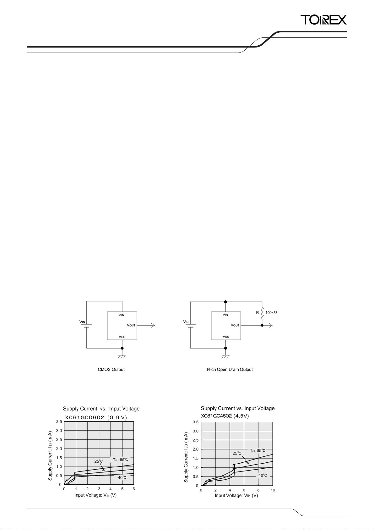
■TYPICAL APPLICATION CIRCUITS
■TYPICAL PERFORMANCE CHARACTERISTICS
1.6V~6.0V)
DF
■FEATURES
Highly Accurate : ±2%
Low Power Consumption
Detect Voltage Range : 0.8V ~ 1.5V in 0.1V
increments (Low Voltage)
: 1.6V~6.0V in 0.1V
increments (Standard Voltage)
Operating Voltage Range
:
Detect Voltage Temperature characteristics
: ±100ppm/℃ (TYP.)
Output Configuration : N-ch open drain output or CMOS
Operating Ambient Temperature : -40℃~+85℃
Package USP-3
Environmentally Friendly: EU RoHS Compliant, Pb Free
: 0.7 μA [ VIN=1.5V ] (TYP.)
: 0.7V ~ 6.0V (Low Voltage)
0.7V~10.0V (Standard Voltage)
1/16
XC61G Series
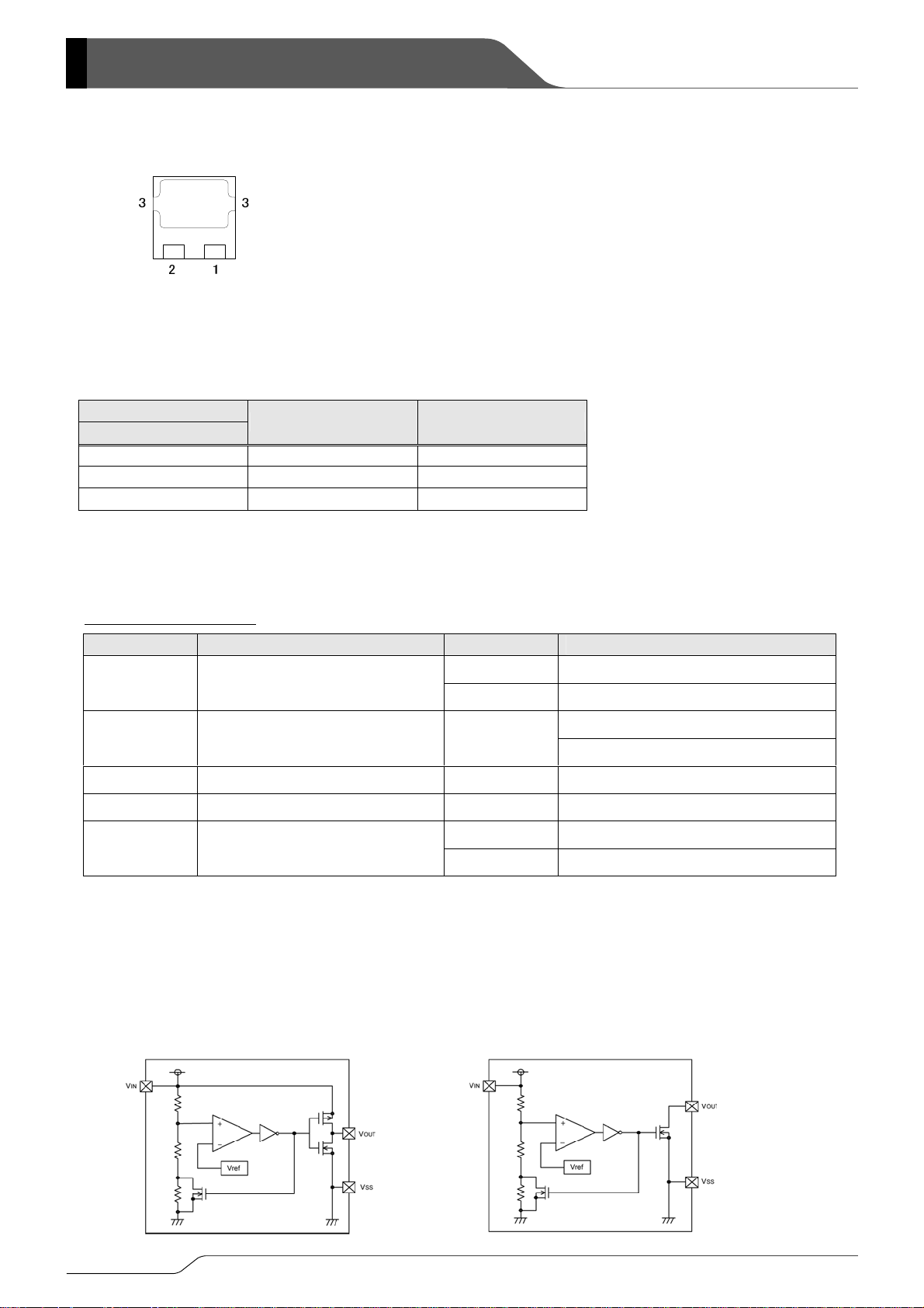
■PIN CONFIGURATION
VIN
OUT
V
V
(BOTTOM VIEW)
■PIN ASSIGNMENT
PIN NUMBER
USP-3
3 VIN
1 VSS Ground
2 VOUT Output
■PRODUCT CLASSIFICATION
●Ordering Information
XC61G ①②③④⑤⑥⑦-⑧
V
IN
SS
PIN NAME FUNCTION
(*1)
Supply Voltage
DESIGNATOR ITEM SYMBOL DESCRIPTION
C CMOS output
①
Output Configuration
N N-ch open drain output
e.g. 0.8V → ②0, ③8
②③
Detect Voltage 08 ~ 60
e.g. 1.5V → ②1, ③5
④
⑤
⑥⑦-⑧
(*1)
The “-G” suffix indicates that the products are Halogen and Antimony free as well as being fully RoHS compliant.
■BLOCK DIAGRAMS
(1) CMOS Output (2) N-ch Open Drain Output
Output Delay 0 No delay
Detect Accuracy 2
Packages
(Order Unit)
HR
HR-G
Within ± 2%
USP-3
USP-3
(3,000/Reel)
(3,000/Reel)
2/16

■ABSOLUTE MAXIMUM RATINGS
PAR AMET ER SYMBOL RATINGS UNITS
Input Voltage
Output Current
*1 VSS-0.3 ~ 9.0
*2
*1 50
*2
CMOS VSS -0.3 ~ VIN +0.3
Output Voltage
N-ch Open Drain Output *1 VSS -0.3 ~ 9.0
N-ch Open Drain Output *2
Power Dissipation
USP-3 Pd 120 mW
Operating Ambient Temperature Topr
Storage Temperature Range Tstg
■ELECTRICAL CHARACTERISTICS
V
= 0.8 to 6.0V ± 2%
DF(T)
PAR AMET ER SYMBOL CONDITIONS MIN. TYP. MAX.
V
=0.8V~1.5V*1
Detect Voltage VDF
DF(T)
V
=1.6V~6.0V*2
DF(T)
Hysteresis Range VHYS
VIN = 1.5V
VIN = 2.0V - 0.8 2.7
Supply Current ISS
VIN = 3.0V - 0.9 3.0
VIN = 4.0V - 1.0 3.2
= 5.0V - 1.1 3.6
V
IN
Operating Voltage VIN
Output Current
VDF(T) = 0.8V to 1.5V 0.7 - 6.0
V
DF(T) = 1.6V to 6.0V 0.7 - 10.0
N-ch, VDS = 0.5V
(Low Voltage)
CMOS, P-ch, VDS=2.1V
I
OUT
Output Current
N-ch, VDS = 0.5V
(Standard Voltage)
CMOS,
P-ch, VDS=2.1V
CMOS
Leakage
Current
N-ch Open
Temperature
Characteristics
Delay Time
(VDR → VOUT inversion)
NOTE:
*
1:Low Voltage (V
*
2:Standard Voltage (V
: Nominal detect voltage
V
DF(T)
Release Voltage: V
Output
(Pch)
Drain
=0.8V~1.5V)
DF(T)
= VDF + V
DR
ΔV
(ΔTopr・V
=1.6V~6.0V)
DF(T)
HYS
I
LEAK
t
DLY
V
VIN=6.0V, V
V
/
DF
DF
-40℃ ≦ Topr ≦ 85℃
)
x0.9, V
IN=VDF
=10.0V, V
IN
DR→VOUT inversion
V
VIN
IOUT
V
-0.3 ~ 12.0
SS
50
VOUT
VSS -0.3 ~ 12.0
-40~+85 ℃
-40~+125 ℃
V
DF
x 0.98
VDF
x 0.02
VDF
VDF
x 0.05
VDF
x 1.02
VDF
x 0.08
- 0.7 2.3
VIN =0.7V 0.10 0.80 -
=1.0V 0.85 2.70 -
V
IN
VIN =6.0V - -7.5 -1.5 4
VIN =1.0V
VIN =2.0V
VIN =3.0V
VIN =4.0V
V
=5.0V
IN
1.0 2.2 -
3.0 7.7 -
5. 0 10.1 -
6.0 11.5 -
7.0 13.0 -
VIN =8.0V - -10.0 -2.0
=0V - -10 -
OUT
=6.0V*1
OUT
OUT
=10.0V*2
- 10 100
-
±100
-
- 0.03 0.2 ms 5
XC61G
Series
Ta = 2 5 ℃
V
mA
V
UNITS
V 1
V 1
μA
V 1
mA
nA 3
ppm/
℃
Ta =2 5℃
CIRCUITS
2
3
3
4
1
3/16
XC61G Series
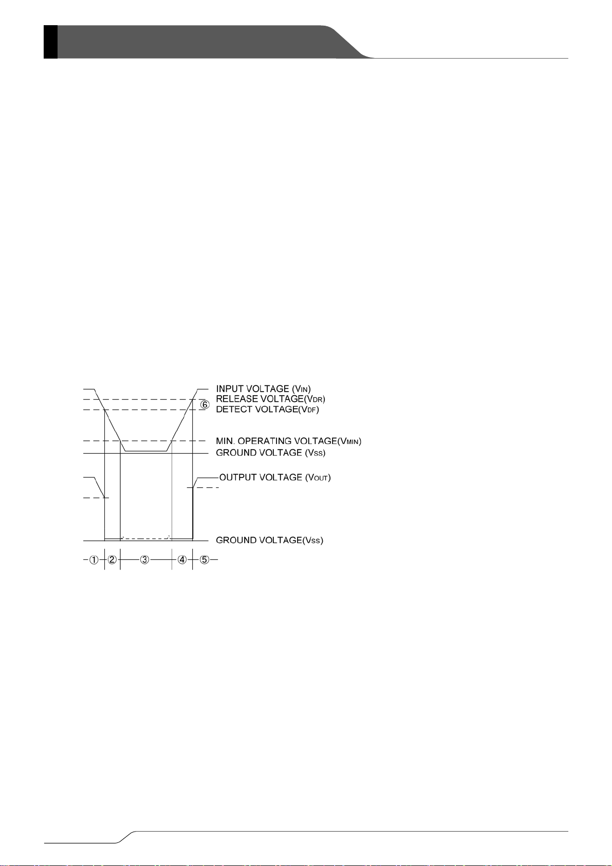
■OPERATIONAL EXPLANATION
●CMOS output
① When input voltage (VIN) is higher than detect voltage (VDF), output voltage (VOUT) will be equal to VIN.
(A condition of high impedance exists with N-ch open drain output configurations.)
② When input voltage (VIN) falls below detect voltage (VDF), output voltage (VOUT) will be equal to the ground voltage
(VSS) level.
③ When input voltage (V
IN) falls to a level below that of the minimum operating voltage (VMIN), output will become
unstable. (As for the N-ch open drain product of XC61CN, the pull-up voltage goes out at the output voltage.)
④ When input voltage (V
IN) rises above the ground voltage (VSS) level, output will be unstable at levels below the
minimum operating voltage (VMIN). Between the VMIN and detect release voltage (VDR) levels, the ground voltage (VSS)
level will be maintained.
⑤ When input voltage (V
IN) rises above detect release voltage (VDR), output voltage (VOUT) will be equal to VIN.
(A condition of high impedance exists with N-ch open drain output configurations.)
⑥ The difference between V
DR and VDF represents the hysteresis range.
●Timing Chart
4/16
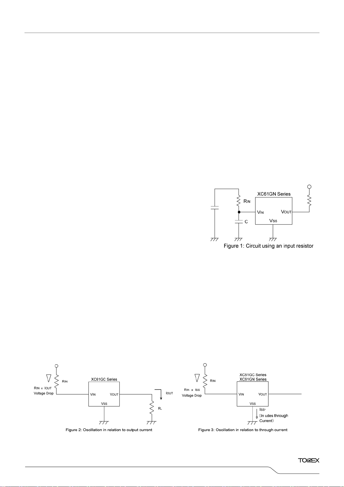
■NOTES ON USE
1. Please use this IC within the stated absolute maximum ratings. For temporary, transitional voltage drop or voltage rising
phenomenon, the IC is liable to malfunction should the ratings be exceeded.
2. When a resistor is connected between the V
occur as a result of voltage drops at R
3. When a resistor is connected between the V
N-ch open-drain output configurations, oscillation may occur as a result of through current at the time of voltage release even
If load current (I
4. Please use N-ch open drain output configuration, when a resistor RIN is connected between the VIN pin and power source.
In such cases, please ensure that RIN is less than 10kΩ and that C is more than 0.1μF, please test with the actual device.
(refer to the Oscillation Description (1) below)
5. With a resistor RIN connected between the VIN pin and the power supply, the VIN pin voltage will be getting lower than the
power supply voltage as a result of the IC's supply current flowing through the V
6. In order to stabilize the IC's operations, please ensure that V
7. Torex places an importance on improving our products and its reliability.
However, by any possibility, we would request user fail-safe design and post-aging treatment on system or equipment.
●Oscillation Description
(1) Load current oscillation with the CMOS output configuration
When the voltage applied at power supply, release operations commence and the detector's output voltage increases.
Load current (IOUT) will flow at RL. Because a voltage drop (RIN x IOUT) is produced at the RIN resistor, located between
the power supply and the V
the voltage level at the V
commence. Following detect operations, load current flow will cease and since voltage drop at R
voltage level at the V
Oscillation may occur with this "release - detect - release" repetition.
Further, this condition will also appear via means of a similar mechanism during detect operations.
(2) Oscillation as a result of through current
Since the XC61G series are CMOS IC
release and detect operations). Consequently, oscillation is liable to occur as a result of drops in voltage at the through
current's resistor (RIN) during release voltage operations. (refer to Figure 3 )
Since hysteresis exists during detect operations, oscillation is unlikely to occur.
Power supply
OUT) does not exist. (refer to the Oscillation Description (2) below )
IN pin, the load current will flow via the IC's VIN pin. The voltage drop will also lead to a fall in
IN pin. When the VIN pin voltage level falls below the detect voltage level, detect operations will
IN pin will rise and release operations will begin over again.
IN pin and the power supply with CMOS output configurations, oscillation may
IN if load current (IOUT) exists. (refer to the Oscillation Description (1) below)
IN pin and the power supply with CMOS output configurations, irrespective of
IN pin.
IN pin input frequency's rise and fall times are more than 2 μ s/ V.
Power supply
IN will disappear, the
S, through current will flow when the IC's internal circuit switching operates (during
Power supply
XC61G
Series
5/16

XC61G Series
■TEST CIRCUITS
6/16

■TYPICAL PERFORMANCE CHARACTERISTICS
●Low Voltage
XC61G
Series
Note: Unless otherwise stated, the N-ch open drain pull-up resistance value is 100kΩ.
7/16

XC61G Series
■TYPICAL PERFORMANCE CHARACTERISTICS (Continued)
●Low Voltage (Continued)
8/16

■TYPICAL PERFORMANCE CHARACTERISTICS (Continued)
●Standard Voltage
XC61G
Series
9/16

)
V
XC61G Series
■TYPICAL PERFORMANCE CHARACTERISTICS (Continued)
●Standard Voltage (Continued)
Note: Unless otherwise stated, the N-ch open drain pull-up resistance value is 100kΩ.
XC61GC4502 (4.5V)
80
70
60
(mA
50
OUT
40
30
20
Output Current: I
10
0
XC61CC4502 (4.5V品)
Ta=25℃
V
=4.0V
IN
1.5V
0 0.51.01.5 2.02.53.03.54.0
V
3.5V
3.0
2.5V
2.0V
(V)
DS
10/16

)
■TYPICAL PERFORMANCE CHARACTERISTICS(Continued
●Standard Voltage (Continued)
XC61G
Series
11/16

)
XC61G Series
■TYPICAL PERFORMANCE CHARACTERISTICS(Continued
●Standard Voltage (Continued)
12/16

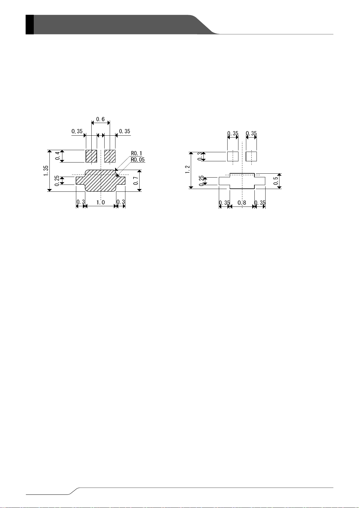
■PACKAGING INFORMATION
●USP-3
XC61G
Series
13/16
XC61G Series
■PACKAGING INFORMATION (Continued)
●USP-3
Reference Pattern Layout Dimension
Reference metal mask design
14/16

■MARKING RULE
●USP-3
USP-3
(TOP VIEW)
① represents integer of output voltage and detect voltage
CMOS Output (XC61GC series) N-ch Open Drain Output (XC61GN series)
MARK VOLTAGE (V)
MARK
VOLTAGE (V)
A 0.X K 0.X
B 1.X L 1.X
C 2.X M 2.X
D 3.X N 3.X
E 4.X P 4.X
F 5.X R 5.X
H 6.X S 6.X
② represents decimal number of detect voltage
MARK
VOLTAGE (V)
PRODUCT SERIES
Ex:
3 X.3 XC61G**3
0 X.0 XC61G**0
③ represents delay time
MARK
Delay Time
PRODUCT SERIES
3 No XC61G***0
④ represents production lot number
0 to 9,A to Z reverse character 0 to 9, A to Z repeated
(G, I, J, O, Q, W excluded)
XC61G
Series
15/16

XC61G Series
1. The products and product specifications contained herein are subject to change without
notice to improve performance characteristics. Consult us, or our representatives
before use, to confirm that the information in this datasheet is up to date.
2. We assume no responsibility for any infringement of patents, patent rights, or other
rights arising from the use of any information and circuitry in this datasheet.
3. Please ensure suitable shipping controls (including fail-safe designs and aging
protection) are in force for equipment employing products listed in this datasheet.
4. The products in this datasheet are not developed, designed, or approved for use with
such equipment whose failure of malfunction can be reasonably expected to directly
endanger the life of, or cause significant injury to, the user.
(e.g. Atomic energy; aerospace; transport; combustion and associated safety
equipment thereof.)
5. Please use the products listed in this datasheet within the specified ranges.
Should you wish to use the products under conditions exceeding the specifications,
please consult us or our representatives.
6. We assume no responsibility for damage or loss due to abnormal use.
7. All rights reserved. No part of this datasheet may be copied or reproduced without the
prior permission of TOREX SEMICONDUCTOR LTD.
16/16
 Loading...