


XC61C Series
ETR0201_013a
Low Voltage Detectors (VDF= 0.8V~1.5V)
Standard Voltage Detectors (V
■GENERAL DESCRIPTION
The XC61C series are highly precise, low power consumption voltage detectors, manufactured using CMOS and laser
trimming technologies.
Detect voltage is extremely accurate with minimal temperature drift.
Both CMOS and N-channel open drain output configurations are available.
■APPLICATIONS
●Microprocessor reset circuitry
●Memory battery back-up circuits
●Power-on reset circuits
●Power failure detection
●System battery life and charge voltage monitors
■TYPICAL APPLICATION CIRCUITS
■TYPICAL PERFORMANCE CHARACTERISTICS
1.6V~6.0V)
DF
■FEATURES
Highly Accurate : ± 2%
± 1%(Standard Voltage VD: 2.6V~5.0V)
Low Power Consumption : 0.7μA (TYP.) [V
Detect Voltage Range : 0.8V ~ 6.0V in 0.1V increments
Operating Voltage Range : 0.7V ~ 6.0V (Low Voltage)
0.7V~10.0V (Standard Voltage)
Detect Voltage Temperature Characteristics
: ±100ppm/℃ (TYP.)
Output Configuration : N-channel open drain or CMOS
Packages : SSOT-24
SOT-23
SOT-89
TO-92
Environmentally Friendly : EU RoHS Compliant, Pb Free
:
IN=1.5V]
1/17

XC61C Series
■PIN CONFIGURATION
■PIN ASSIGNMENT
(SIDE VIEW) (SIDE VIEW)
PIN NUMBER
SSOT-24 SOT-23 SOT-89 TO-92 (T) TO-92 (L)
2 3 2 2 1 VIN
PIN NAME FUNCTION
Supply Voltage
4 2 3 3 2 VSS Ground
1 1 1 1 3 VOUT Output
3 - - - - NC No Connection
■PRODUCT CLASSIFICATION
●Ordering Information
XC61C①②③④⑤⑥⑦-⑧
DESIGNATOR DESCRIPTION SYMBOL DESCRIPTION
① Output Configuration
② ③ Detect Voltage 08 ~ 60
④ Output Delay 0 No delay
⑤ Detect Accuracy
⑥⑦-⑧
(*1)
The “-G” suffix indicates that the products are Halogen and Antimony free as well as being fully RoHS compliant.
(*2)
The device orientation is fixed in its embossed tape pocket. For reverse orientation, please contact your local Torex sales office or
representative. (Standard orientation: ⑥R-⑧, Reverse orientation: ⑥L-⑧)
(*1)
Packages
Taping Type
(*2)
C CMOS output
N N-ch open drain output
e.g.0.9V → ②0, ③9
e.g.1.5V → ②1, ③5
1 Within ±1% (V
=2.6V~5.0V)
DF(T)
2 Within ±2%
NR SSOT-24 (SC-82)
NR-G SSOT-24 (SC-82) (Halogen & Antimony free)
MR SOT-23
MR-G SOT-23 (Halogen & Antimony free)
PR SOT-89
PR-G SOT-89 (Halogen & Antimony free)
TH TO-92 (Standard) Taping Type: Paper type
TB TO-92 (Standard) Taping Type: Bag
LH
LB
(Custom pin configuration)
TO-92
(Discontinued Product)
(Custom pin configuration)
TO-92
(Discontinued Product)
Taping Type: Paper type
Taping Type: Bag
2/17
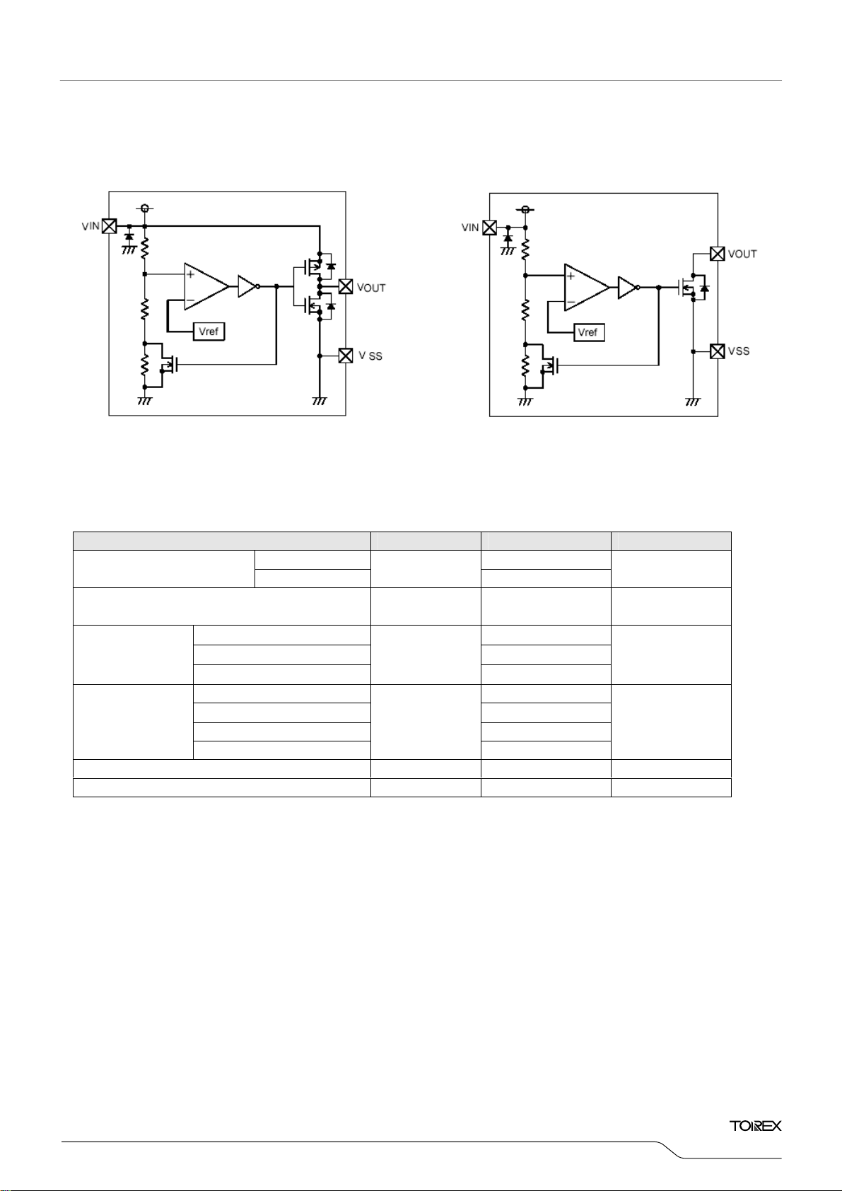
■BLOCK DIAGRAMS
(1) CMOS Output (2) N-ch Open Drain Output
■ABSOLUTE MAXIMUM RATINGS
PAR AMETER SYMBOL RATINGS UNITS
Input Voltage
*1 9.0
*2
VIN
12.0
Output Current IOUT 50 mA
CMOS VSS -0.3 ~ VIN +0.3
Output Voltage
N-ch Open Drain Output *1 VSS -0.3 ~ 9.0
N-ch Open Drain Output *2
VOUT
VSS -0.3 ~ 12.0
SSOT-24 150
Power Dissipation
SOT-23 150
SOT-89 500
TO-92
Operating Temperature Range Topr
Storage Temperature Range Tstg
Pd
300
-40~+85
-40~+125
*1: Low voltage: VDF(T)=0.8V~1.5V
*2: Standard voltage: VDF(T)=1.6V~6.0V
Ta = 25OC
V
V
mW
O
C
O
C
XC61C
Series
3/17

XC61C Series
■ELECTRICAL CHARACTERISTICS
VDF (T) = 0.8V to 6.0V ± 2%
VDF (T) = 2.6V to 5.0V ± 1%
PAR AMETER SYMBOL CONDITIONS MIN. TYP. MAX.
VDF(T)=0.8V~1.5V *1
V
Detect Voltage VDF
DF(T)=1.6V~6.0V *2
DF(T)=2.6V~5.0V *2
V
Hysteresis Range VHYS
VIN = 1.5V
VIN = 2.0V
Supply Current ISS
VIN = 3.0V
VIN = 4.0V
VIN = 5.0V
Operating Voltage *1 VDF(T) = 0.8V to 1.5V 0.7 - 6.0
Operating Voltage *2
Output Current *1
VIN
CMOS, P-ch V
V
DF(T) = 1.6V to 6.0V 0.7 - 10.0
N-ch VDS = 0.5V
DS = 2.1V VIN = 6.0V - -7.5 -1.5 4
VIN = 0.7V
IN = 1.0V 0.85 2.70
V
VIN = 1.0V
OUT
Output Current *2
I
N-ch VDS = 0.5V
VIN = 2.0V 3.0
VIN = 3.0V 5.0 10.1
VIN = 4.0V 6.0 11.5
IN = 5.0V 7.0 13.0
V
CMOS, P-ch VDS = 2.1V VIN = 8.0V
Leak Current Ileak
Temperature
Characteristics
Delay Time
(VDR→
V
OUT
inversion)
NOTE:
*1: Low Voltage: V
*2: Standard Voltage: V
DF (T): Setting detect voltage
V
Release Voltage: V
DF(T)=0.8V~1.5V
DR = VDF + VHYS
VIN=6.0V, VOUT=6.0V*1
V
IN=10.0V, VOUT=10.0V*2
ΔV
Δ
Top r・VDF
DF
-40℃ ≦ Topr ≦ 85℃
tDLY Inverts from VDR to VOUT - 0.03 0.20 ms 5
DF(T)=1.6V~6.0V
CMOS - 10 -
N-ch Open Drain - 10 100
DF(T)
V
x 0.98
VDF(T)
x 0.99
VDF
x 0.02
DF(T)
V
DF(T)
V
VDF
x 0.05
- 0.7 2.3
- 0.8 2.7
- 0.9 3.0
- 1.0 3.2
- 1.1 3.6
0.10 0.80 -
1.0
2.2
7.7 -
- -10.0 -2.0
-
±100
VDF(T)
x 1.02
VDF(T)
x 1.01
VDF
x 0.08
-
-
-
-
-
-
Ta =2 5℃
CIRCUITS
UNITS
V 1
V 1
V 1
μA
2
V 1
3
mA
3
4
nA 3
ppm/
℃
-
4/17

■OPERATIONAL EXPLANATION
(Especially prepared for CMOS output products)
① When input voltage (VIN) rises above detect voltage (VDF), output voltage (VOUT) will be equal to VIN.
(A condition of high impedance exists with N-ch open drain output configurations.)
② When input voltage (V
SS) level.
(V
IN) falls below detect voltage (VDF), output voltage (VOUT) will be equal to the ground voltage
③ When input voltage (VIN) falls to a level below that of the minimum operating voltage (VMIN), output will become
unstable. In this condition, V
IN will equal the pulled-up output (should output be pulled-up.)
④ When input voltage (VIN) rises above the ground voltage (VSS) level, output will be unstable at levels below the
minimum operating voltage (V
MIN). Between the VMIN and detect release voltage (VDR) levels, the ground voltage (VSS)
level will be maintained.
⑤ When input voltage (V
IN) rises above detect release voltage (VDR), output voltage (VOUT) will be equal to VIN.
(A condition of high impedance exists with N-ch open drain output configurations.)
⑥ The difference between V
DR and VDF represents the hysteresis range.
●Timing Chart
XC61C
Series
5/17
XC61C Series
■NOTES ON USE
1. Please use this IC within the stated maximum ratings. Operation beyond these limits may cause degrading or permanent
damage to the device.
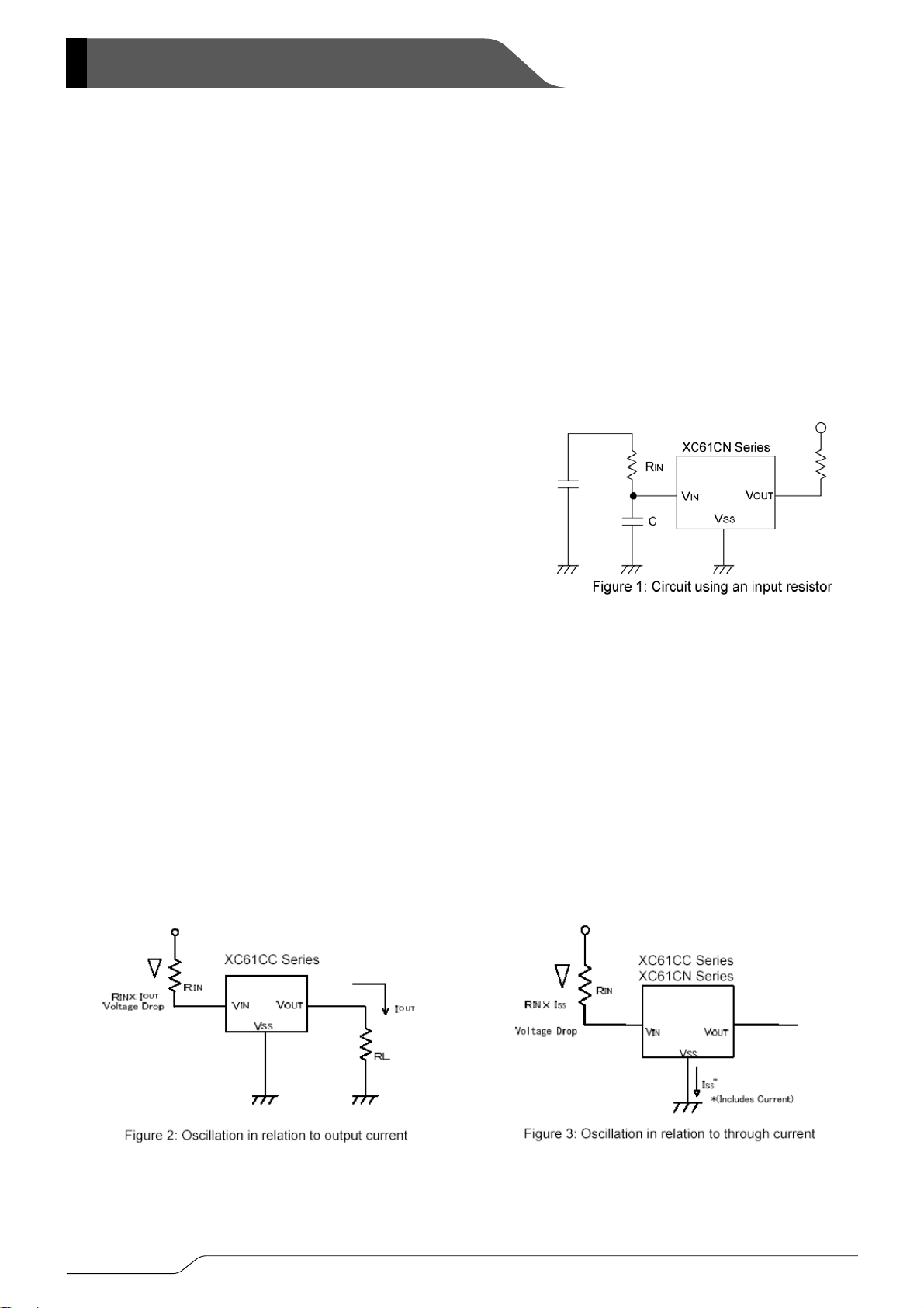
2. When a resistor is connected between the VIN pin and the input with CMOS output configurations, oscillation may occur
as a result of voltage drops at R
3. When a resistor is connected between the V
output configurations, oscillation may occur as a result of through current at the time of voltage release even if load
current (IOUT) does not exist. (refer to the Oscillation Description (2) below )
4. With a resistor connected between the V
supply current flowing through the V
5. In order to stabilize the IC's operations, please ensure that V
several μ sec / V.
6. Please use N-ch open drains configuration, when a resistor RIN is connected between the VIN pin and power source.
In such cases, please ensure that R
●Oscillation Description
(1) Output current oscillation with the CMOS output configuration
When the voltage applied at IN rises, release operations commence and the detector's output voltage increases. Load
current (IOUT) will flow at RL. Because a voltage drop (RIN x IOUT) is produced at the RIN resistor, located between the input
(IN) and the V
at the V
Following detect operations, load current flow will cease and since voltage drop at R
the V
IN pin will rise and release operations will begin over again.
Oscillation may occur with this " release - detect - release " repetition.
Further, this condition will also appear via means of a similar mechanism during detect operations.
(2) Oscillation as a result of through current
Since the XC61C series are CMOS IC
release and detect operations). Consequently, oscillation is liable to occur as a result of drops in voltage at the through
current's resistor (RIN) during release voltage operations. (refer to Figure 3)
Since hysteresis exists during detect operations, oscillation is unlikely to occur.
IN pin, the load current will flow via the IC's VIN pin. The voltage drop will also lead to a fall in the voltage level
IN pin. When the VIN pin voltage level falls below the detect voltage level, detect operations will commence.
IN if load current (IOUT) exists. (refer to the Oscillation Description (1) below)
IN pin and the input with CMOS output configurations, irrespective of N-ch
IN pin and the input, detect and release voltage will rise as a result of the IC's
IN pin.
IN pin's input frequency's rise and fall times are more than
IN is less than 10kΩ and that C is more than 0.1μF.
IN will disappear, the voltage level at
S, through current will flow when the IC's internal circuit switching operates (during
6/17
 Loading...