


XC6127 Series
Ultra Small Voltage Detector with High Precision Delay Circuit and Manual Reset Function
■GENERAL DESCRIPTION
XC6127 series is ultra small highly accurate voltage detector with delay circuit built-in.
The device includes a highly accurate reference voltage source, manufactured using CMOS process technology and laser
trimming technologies, it maintains high accuracy, low power consumption, and accurate releases delay time over the full
operation temperature range.
The release delay time periods are internally set in a range from 50ms to 800ms.
Moreover, with the manual reset function, reset can be asserted at any time.
The device is available in both CMOS and N-channel open drain output configurations. Also detect logic is available in both
RESETB (Active Low) and RESET (Active High).
Ultra small package USPN-4 is ideally suited for small design of portable devices and high densely mounting applications.
The conventional packages SSOT-24,SOT-25 is also available for upper compatible replacements.
■APPLICATIONS
● Microprocessor logic reset circuitry
● System battery life and charge voltage monitors
● Memory battery back-up circuits
● Power-on reset circuits
● Power failure Detection
● Delay circuit
■TYPICAL APPLICATION CIRCUIT
V
IN
RESET
SW
XC6127 series
RESETB
V
IN
RESET
MRB
V
SS
VCC
μP
RESETB/RESET
INPUT
VSS
V
IN
RESET
SW
CMOS output
XC6127 series
RESETB
V
IN
RESET
MRB
V
SS
Vpull-Up
Rpull
RESETB/RESET
INPUT
VCC
μP
VSS
■FEATURES
High Accuracy
Temperature Characteristics
Low Power Consumption
Operating Voltage Range
Detect Voltage Range
Manual Reset Input
Output Configuration
Output Logic
Release Delay Time
Operating Ambient Temperature
Packages
Environmentally Friendly
: ±0.8% (25℃)
: ±50ppm/℃
0.6μA TYP. (Detect: VDF=1.8V, VIN=1.62V)
:
0.7μA TYP. (R e lea se: VDF=1.8V, VIN=1.98V)
: 0.7V~6.0V
: 1.5V~5.5V (0.1V increments)
MRB Pin (Built-in Pull-up resistance)
:
N-channel open drain or CMOS
:
RESETB (Active Low)
:
RESET (Active High)
50ms/100ms/200ms/400ms/800ms±15%
:
: : -40℃ ~ +85℃
USPN-4, SSOT-24, SOT-25
EU RoHS Compliant, Pb Free
:
■ TYPICAL PERFORMANCE
CHARACTERISTICS
XC6127x27Bx
VIN=V
×0.9→V
DFL
(ms)
DR
115
110
105
100
95
90
Release Delay Time: t
85
-50 -25 0 25 50 75 100
Ambient Temperature: Ta (℃)
×1.1 , MRB=O PEN
DFL
ETR0217-006
N-ch open drain output
1/24

XC6127 Series
■PIN CONFIGURATION
V
V
IN
V
SS
RESETB
14
RESET
MRB
23
RESETB
RESET
MRB
34
1
V
IN
2
V
SS
USPN-4
(BOTTOM VIEW)
SSOT-24
(TOP VIEW)
■PIN ASSIGNMENT
PIN NUMBER
USPN-4 SSOT-24 SOT-25
PIN NAME FUNCTIONS
1 4 4 RESETB Signal Output (Active Low)
1 4 4 RESET Signal Output (Active High)
2 3 1 MRB Manual Reset Input
3 2 2 VSS Ground
4 1 5 VIN Power Input
(*1) Type A~E (Refer to the ④ in Ordering Information table)
(*2) Type F~K (Refer to the ④ in Ordering Information table)
■FUNCTION CHART
PIN NAME SIGNAL STATUS
L Forced Reset
MRB
H Normal Operation
OPEN Normal Operation
IN
5 4
1
MRB NC
2
V
SS
SOT-25
(TOP VIEW)
RESETB
RESET
(*1)
(*2)
3
2/24

■PRODUCT CLASSIFICATION
●Ordering Information
XC6127①②③④⑤⑥-⑦
(*1)
DESIGNATOR ITEM SYMBOL DESCRIPTION
①
②③
Output Configuration
Detect Voltage
C CMOS output
N N-ch open drain output
15~55 e.g. 2.7V → ②=2, ③=7
A Reset Active Low, Release Delay Time: 50ms
B Reset Active Low, Release Delay Time: 100ms
C Reset Active Low, Release Delay Time: 200ms
D Reset Active Low, Release Delay Time: 400ms
④
Type
E Reset Active Low, Release Delay Time: 800ms
F Reset Active High, Release Delay Time: 50ms
G Reset Active High, Release Delay Time: 100ms
H Reset Active High, Release Delay Time: 200ms
J Reset Active High, Release Delay Time: 400ms
K Reset Active High, Release Delay Time: 800ms
7R-G USPN-4 (5,000/Reel)
MR-G SOT-25 (3,000/Reel)
⑤⑥-⑦
(*1)
Packages (Order Unit)
NR-G SSOT-24 (3,000/Reel)
(*1)
The “-G” suffix denotes Halogen and Antimony free as well as being fully RoHS compliant.
XC6127
Series
3/24

XC6127 Series
■BLOCK DIAGRAMS
1) XC6127 Series, Type CxxA/CxxB/CxxC/CxxD/CxxE (CMOS Output, Output Logic: Active Low)
2) XC6127 Series, Type NxxA/NxxB/NxxC/NxxD/NxxE (N-ch Open Drain Output, Output Logic: Active Low)
4/24
* Diodes inside the circuits are ESD protection diodes and parasitic diodes.
* Diodes inside the circuits are ESD protection diodes and parasitic diodes.

■BLOCK DIAGRAMS (Continued)
3) XC6127 Series, Type CxxF/CxxG/CxxH/CxxJ/CxxK (CMOS Output, Output Logic: Active High)
4) XC6127 Series, Type NxxF/NxxG/NxxH/NxxJ/NxxK (N-ch Open Drain Output, Output Logic: Active High)
* Diodes inside the circuits are ESD protection diodes and parasitic diodes.
* Diodes inside the circuits are ESD protection diodes and parasitic diodes.
XC6127
Series
5/24

XC6127 Series
■ABSOLUTE MAXIMUM RATINGS
PAR AMETER SYMBOL RATINGS UNITS
Input Voltage VIN
MRB Input Voltage V
Output Current
MRB
(*1)
VSS-0.3~VSS+6.5
VSS~VSS+6.5
20 mA
Ta =2 5℃
V
V
(*2)
(*3)
Output Voltage
XC6127C
XC6127N
USPN-4 100
Power Dissipation
SOT-25 250
SSOT-24
Operating Ambient Temperature Topr
Storage Temperature Tst g
Note:
(*1) SYMBOL is different for each product.
I
I
(*2) CMOS Output
(*3) N-ch Open Drain Output
(*4) SYMBOL is different for each product.
V
V
: Type XC6127CxxA/CxxB/CxxC/CxxD/CxxE, Type XC6127NxxA/NxxB/NxxC/NxxD/NxxE
RBOUT
: Type XC6127CxxF/CxxG/CxxH/CxxJ/CxxK, Type XC6127NxxF/NxxG/NxxH/NxxJ/NxxK
ROUT
: Type XC6127CxxA/CxxB/CxxC/CxxD/CxxE, Type XC6127NxxA/NxxB/NxxC/NxxD/NxxE
RESETB
: Type XC6127CxxF/CxxG/CxxH/CxxJ/CxxK, Type XC6127NxxF/NxxG/NxxH/NxxJ/NxxK
RESET
(*4)
Pd
VSS-0.3~VIN+0.3≦VSS+6.5
V
VSS-0.3~VSS+6.5
mW
150
-40~+85 ℃
-55~+125 ℃
6/24

■ELECTRICAL CHARACTERISTICS
●XC6127CxxA/CxxB/CxxC/CxxD/CxxE, XC6127NxxA/NxxB/NxxC/NxxD/NxxE (Output Logic: Active Low)
PARAMETER SYMBOL CONDITIONS MIN. TYP. MAX. UNITS CIRCUIT
Operating Voltage VIN
Detect Voltage V
Hysteresis Width V
DFL
HYS
(*1)
V
=1.5~5.5V, MRB=OPEN
DF(T)
V
=1.5~5.5V, MRB=OPEN
DF(T)
(*2)
0.7
V
×0.992 V
DF(T)
V
×0.02 V
DFL
(*3)
DF(T)
(*4)
E-1
×0.05 V
DFL
6.0 V -
V
DF(T)
×1.008
×0.08
DFL
V ①
V ①
XC6127
Series
Ta =2 5 ℃
Supply Current 1 I
Supply Current 2 I
RESETB
Output Current
RESETB
Leakage
Current
CMOS
Output(Pch)
Nch Open
Drain Output
Temperature Characteristics
Detect Delay Time
(*11)
SS1
SS2
I
RBOUT1
I
RBOUT2
I
LEAK
ΔV
DFL
(ΔTopr・V
tDF
(*10)
/
DFL
)
VIN=V
VIN=V
VIN=0.7V, V
VIN=1.0V, V
(*6)
VIN=2.0V
(*7)
VIN=3.0V
(*8)
VIN=4.0V
(*9)
VIN=5.0V
VIN=6.0V, V
VIN=V
×0.9, V
DFL
VIN=6.0V, V
VIN=V
DFL
×0.9 , MRB=OPEN
DFL
V
=1.5~1.8V - 0.6 1.4
DF(T)
V
=1.9~3.0V - 0.7 1.6
DF(T)
V
=3.1~5.5V - 1.0 1.9
DF(T)
(*5)
×1.1
DFL
V
V
V
RESETB
RESETB
, V
, V
, V
, V
RESETB
, MRB=OPEN
=1.5~1.8V - 0.7 1.6
DF(T)
=1.9~3.0V - 0.8 1.9
DF(T)
=3.1~5.5V - 1.1 2.35
DF(T)
=0.5V(Nch) , MRB=OPEN
=0.5V(Nch) , MRB=OPEN
=0.5V(Nch) , MRB=OPEN
RESETB
=0.5V(Nch) , MRB=OPEN
RESETB
=0.5V(Nch) , MRB=OPEN
RESETB
=0.5V(Nch) , MRB=OPEN
RESETB
=5.5V(Pch) , MRB=OPEN
=0V , MRB=OPEN
RESETB
0.014 0.2 -
0.5 1.6 -
4.4 7.0 -
7.0 9.0 -
8.5 11.0 -
9.0 12.0 -
- -4.5 -3.0 mA ③
- -0.01 - μA
μA ②
μA ②
mA ③
③
=6.0V , MRB=OPEN
RESETB
- 0.01 0.15 μA
-40℃≦Topr≦85℃ - ±50 - ppm/℃ ①
DFL
×0.9
(*11)
, MRB=OPEN
- - 100 μs ④
×1.1→V
Release Delay Time
MRB “Low” Level Voltage
MRB “High” Level Voltage
MRB pull-up Resistance R
Minimum MRB Pulse Width
(*12)
(*14)
(*14)
tDR
V
V
MRL
V
V
MRH
0.4 0.8 3.0 MΩ ⑥
MRB
T
MRB
VIN=V
×0.9→V
DFL
×1.1
DFL
×1.1≦VIN≦6.0V VSS - 0.3 V ⑤
DFL
×1.1≦VIN≦6.0V 1.0 - 6.0 V ⑤
DFL
V
=6.0V,
IN
Applied pulse to MRB pin,
Note:
(*1) V
(*2) For the N-ch Open Drain, Rpull=100kΩ, Vpull-Up=V
Rpull: An External Pull-up resistor
Vpull-Up: Pull-up Voltage
(*3) V
(*4) For the detail value, please refer to “Voltage Table” in P10.
(*5) V
(*6) For V
(*7) For V
(*8) For V
(*9) For V
(*10) For the XC6127C (CMOS output)
(*11) A time between V
(*12) A time between V
: Nominal detect voltage
DF(T)
voltage for V
IN
= 5.5V where VIN=6.0V
DF(T)
>2.0V products.
DF(T)
>3.0V products.
DF(T)
>4.0V products.
DF(T)
>5.0V products.
DF(T)
≦0.3V is under detect state.
OUT
IN=VDFL
IN=VDFL+VHYS
and V
RESETB=VDFL
and V
RESETB=VDFL
IN
×0.45 when VIN falls.
×0.55 when VIN rises.
(*13) For the detail value, please refer to “Release Delay Time” in P11.
(*14) For MRB pin, please do not apply the voltage below V
.
SS
(*12)
, MRB=OPEN
(*13)
E-2
ms ④
150 - - ns ⑦
7/24

XC6127 Series
■ELECTRICAL CHARACTERISTICS (Continued)
●XC6127CxxF/CxxG/CxxH/CxxJ/CxxK, XC6127NxxF/NxxG/NxxH/NxxJ/NxxK (Output Logic: Active High)
PARAMETER SYMBOL CONDITIONS MIN. TYP. MAX. UNITS CIRCUIT
Operating Voltage VIN
Detect Voltage V
DFH
(*1)
V
=1.5~5.5V, MRB=OPEN
DF(T)
V
=1.5~5.5V, MRB=OPEN
DF(T)
(*2)
(*3)
0.7
6.0 V -
V
×0.992
DF(T)
V
E-1
DF(T)
(*4)
Ta =2 5 ℃
V
×1.008
DF(T)
V ①
Hysteresis Width V
Supply Current 1 I
Supply Current 2 I
RESET
Output Current
RESET
Leakage
Current
CMOS
Output (P-ch)
N-ch Open
Drain Output
Temperature
Characteristics
Detect Delay Time
(*16)
t
HYS
SS1
SS2
VIN=1.65V
VIN=2.0V
VIN=3.0V
I
ROUT1
VIN=4.0V
VIN=5.0V
VIN=6.0V, V
VIN=0.7V, V
VIN=1.0V, V
I
ROUT2
(*11)
VIN=2.0V
VIN=3.0V
VIN=4.0V
VIN=5.0V
V
I
LEAK
VIN=V
ΔV
/
DFH
(ΔTopr・V
)
DFH
DF
V
VIN=V
VIN=V
(*7)
(*8)
(*9)
(*10)
(*12)
(*13)
(*14),
(*15)
=6.0V, V
IN
×0.9, V
DFH
×0.02 V
DFH
×0.9 , MRB=OPEN
DFH
V
=1.5~1.8V - 0.6 1.4
DF(T)
V
=1.9~3.0V - 0.7 1.6
DF(T)
V
=3.1~5.5V - 1.0 1.9
DF(T)
(*5)
×1.1
DFH
V
V
V
(*6)
, V
, V
, V
, V
, V
, V
, V
, V
, MRB=OPEN
=1.5~1.8V - 0.7 1.6
DF(T)
=1.9~3.0V - 0.8 1.9
DF(T)
=3.1~5.5V - 1.1 2.35
DF(T)
=0.5V(Nch) , MRB=OPEN
RESET
=0.5V(Nch) , MRB=OPEN
RESET
=0.5V(Nch) , MRB=OPEN
RESET
=0.5V(Nch) , MRB=OPEN
RESET
=0.5V(Nch) , MRB=OPEN
RESET
=0.5V(Nch) , MRB=OPEN
RESET
=0.2V(Pch) , MRB=OPEN
RESET
=0.5V(Pch) , MRB=OPEN
RESET
=1.5V(Pch) , MRB=OPEN
RESET
=2.5V(Pch) , MRB=OPEN
RESET
V
=3.5V(Pch) , MRB=OPEN
RESET
=4.5V(Pch) , MRB=OPEN
RESET
=0V, MRB=OPEN - -0.01 - μA
RESET
=6.0V, MRB=OPEN
RESET
0.5 1.6 -
4.4 7.0 -
7.0 9.0 -
8.5 11.0 -
9.0 12.0 -
9.0 12.0 -
- -0.07 -0.001
- -0.4 -0.09
- -2.0 -1.3
- -3.0 -1.8
- -4.0 -2.5
- -4.5 -3.0
- 0.01 0.15 μA
×0.05 V
DFH
DFH
×0.08
-40℃≦Topr≦85℃ - ±50 - ppm/℃ ①
VIN=V
×1.1→V
DFH
DFH
×0.9
(*16)
, MRB=OPEN
- - E-3
(*17)
μs ④
V ①
μA ②
μA ②
mA ③
mA ③
③
Release Delay Time
MRB “Low” Level Voltage
MRB “High” Level Voltage
MRB pull-up Resistance
Minimum MRB Pulse Width
8/24
(*18)
t
(*20)
(*20)
DR
V
MRL
V
MRH
R
MRB
T
MRB
VIN=V
V
V
DFH
×1.1
(*18)
, MRB=OPEN
×0.9→V
DFH
×1.1≦VIN≦6.0V VSS - 0.3 V ⑤
DFH
×1.1≦VIN≦6.0V 1.0 - 6.0 V ⑤
DFH
(*19)
E-2
ms ④
0.4 0.8 3.0 MΩ ⑥
VIN=6.0V, Applied pulse to MRB pin, 6.0V→0V
150 - - ns ⑦

■ELECTRICAL CHARACTERISTICS (Continued)
(*1) V
(*2) For the N-ch Open Drain, Rpull=100kΩ, Vpull-Up=V
(*3) V
(*4) For the detail value, please refer to “Voltage Table” in P10.
(*5) V
(*6) For V
(*7) For V
(*8) For V
(*9) For V
(*10) For V
(*11) For the XC6127C (CMOS output)
(*12) For V
(*13) For V
(*14) For V
(*15) For V
(*16) A time between V
(*17) For the detail value, please refer to “Detect Delay Time” in P11.
(*18) A time between V
(*19) For the detail value, please refer to “Release Delay Time” in P11.
(*20) For MRB pin, please do not apply the voltage below V
: Nominal detect voltage
DF(T)
Rpull: An External Pull-up resistor
Vpull-Up: Pull-up Voltage
voltage for V
IN
= 5.5V where VIN=6.0V
DF(T)
=1.5V products.
DF(T)
≦1.8V products.
DF(T)
≦2.7V products.
DF(T)
≦3.6V products.
DF(T)
≦4.6V products.
DF(T)
>2.0V products.
DF(T)
>3.0V products.
DF(T)
>4.0V products.
DF(T)
>5.0V products.
DF(T)
≧0.4V is under detect state.
OUT
and V
IN=VDFH
IN=VDFH+VHYS
RESET=VDFH
and V
RESET=VDFH
IN
×0.45 when VIN falls.
×0.55 when VIN rises.
.
SS
XC6127
Series
9/24

)
XC6127 Series
■ELECTRICAL CHARACTERISTICS (Continued
Voltage Table 1
NOMINAL
DETECT
VOLTAGE
(V)
V
DF(T)
DETECT
VOLTAGE
(V) (V)
E-1
V
DFL
or V
V
DFH
MIN. MAX.
1.50 1.4880 1.5120 4.10 4.0672 4.1328
1.60 1.5872 1.6128 4.20 4.1664 4.2336
1.70 1.6864 1.7136 4.30 4.2656 4.3344
1.80 1.7856 1.8144 4.40 4.3648 4.4352
1.90 1.8848 1.9152 4.50 4.4640 4.5360
2.00 1.9840 2.0160 4.60 4.5632 4.6368
2.10 2.0832 2.1168 4.70 4.6624 4.7376
2.20 2.1824 2.2176 4.80 4.7616 4.8384
2.30 2.2816 2.3184 4.90 4.8608 4.9392
2.40 2.3808 2.4192 5.00 4.9600 5.0400
2.50 2.4800 2.5200 5.10 5.0592 5.1408
2.60 2.5792 2.6208 5.20 5.1584 5.2416
2.70 2.6784 2.7216 5.30 5.2576 5.3424
2.80 2.7776 2.8224 5.40 5.3568 5.4432
2.90 2.8768 2.9232 5.50 5.4560 5.5440
3.00 2.9760 3.0240
3.10 3.0752 3.1248
3.20 3.1744 3.2256
3.30 3.2736 3.3264
3.40 3.3728 3.4272
3.50 3.4720 3.5280
3.60 3.5712 3.6288
3.70 3.6704 3.7296
3.80 3.7696 3.8304
3.90 3.8688 3.9312
4.00 3.9680 4.0320
Voltage Table 2
VOLTAGE
NOMINAL
DETECT
(V)
V
DF(T)
DETECT
VOLTAGE
E-1
DFL
or V
DFH
MIN. MAX.
10/24

)
■ELECTRICAL CHARACTERISTICS (Continued
Release Delay Time Table
RELEASE DELAY TIME
(ms)
TYPE
E-2
tDR
MIN. TYP. MAX.
XC6127CxxA / XC6127NxxA 42.5 50 57.5
XC6127CxxB / XC6127NxxB 85 100 115
XC6127CxxC / XC6127NxxC 170 200 230
XC6127CxxD / XC6127NxxD 340 400 460
XC6127CxxE / XC6127NxxE 680 800 920
XC6127CxxF / XC6127NxxF 42.5 50 57.5
XC6127CxxG / XC6127NxxG 85 100 115
XC6127CxxH / XC6127NxxH 170 200 230
XC6127CxxJ / XC6127NxxJ 340 400 460
XC6127CxxK / XC6127NxxK 680 800 920
Detect Delay Time Table
DETECT DELAY TIME
(μs)
TYPE
E-3
tDF
MAX.
XC6127CxxF/CxxG/CxxH/CxxJ/CxxK 100
XC6127NxxF/NxxG/NxxH/NxxJ/NxxK 200
XC6127
Series
11/24

XC6127 Series
■OPERATIONAL EXPLANATION
1. Detect / Release operation using XC6127CxxA/CxxB/CxxC/CxxD/CxxE, XC6127NxxA/NxxB/NxxC/NxxD/NxxE
(Output Logic: Active Low)
●Typical Application Circuit
●Timing Chart
A timing chart is used to explain the operation of the typical application circuit when MRB is open.
①In the initial state, an input voltage (V
While the input voltage (V
*In the case of an N-ch open drain output product, the RESETB pin is in a high-impedance state, and if the output is pulled up, the output
voltage (V
②③After the elapse of the detect delay time (t
(V
RESETB
*This is the same on the N-ch open drain output product.
④The input voltage (V
*When an N-ch open drain output product is used and the output pin is pulled up, an output voltage (V
be output.
⑤The input voltage (V
(V
RESETB
⑥ From the time that the input voltage (V
voltage (V
⑦ After the release delay time (t
*In the case of an N-ch open drain output product, the RESETB pin will be in a high impedance state like ①. If the output is pulled up, an
output voltage (V
⑧The difference between the release voltage (V
) is equal to the pull-up voltage.
RESETB
) equal to the ground voltage (VSS) goes out (detection state).
) is equal to the ground voltage.
) remains at the ground voltage due to the delay circuit.
RESETB
RESETB
) is higher than the detect voltage (V
IN
) drops further, and if it falls below the minimum operating voltage (0.7V), the output becomes undefined state.
IN
) rises past the minimum operating voltage (0.7V), and until it reaches the release voltage (VDR), the output voltage
IN
) equal to the pull-up voltage will be output.
12/24
) higher than the release voltage (VDR) is applied, and then VIN gradually falls.
IN
) that starts when the input voltage (VIN) falls below the detect voltage (V
DF
) becomes higher than the release voltage (VDR) until the release delay time (tDR) elapses, the output
IN
) elapses, the output voltage (V
DR
) and the detect voltage (V
DR
), an output voltage (V
DFL
) is equal to the input voltage (VIN) (release state).
RESETB
) is the hysteresis width (V
DFL
) equal to the input voltage (VIN) goes out.
RESETB
), an output voltage
DFL
) equal to the pull-up voltage may
RESETB
).
HYS

)
XC6127
Series
■OPERATIONAL EXPLANATION(Continued
2. XC6127CxxF/CxxG/CxxH/CxxJ/CxxK, XC6127NxxF/NxxG/NxxH/NxxJ/NxxK (Output Logic: Active High)
●Typical Application Circuit
●Timing Chart
A timing chart is used above to explain the operation of the typical application circuit when MRB is open.
① In the initial state, an input voltage (V
While the input voltage (V
*This is the same on the N-ch open drain output product.
②③After the elapse of the detect delay time (t
voltage (V
*In the case of an N-ch open drain output product, the RESET pin is in a high-impedance state, and if the output is pulled up, the output
voltage (V
④ The input voltage (V
⑤The input voltage (V
(V
RESET
*In the case of an N-ch open drain output product, the RESET pin is in a high-impedance state, and if the output is pulled up, the output
voltage (V
⑥From the time that the input voltage (V
output voltage (V
⑦After the release delay time (t
⑧The difference between the release voltage (V
) is equal to the input voltage (VIN) (detection state).
RESET
) is equal to the pull-up voltage.
RESET
) is equal to the VIN voltage.
) is equal to the pull-up voltage.
RESET
RESET
) is higher than the detect voltage (V
IN
) drops further, and if it falls below the minimum operating voltage (0.7V), the output becomes undefined state.
IN
) rises past the minimum operating voltage (0.7V), and until it reaches the release voltage (VDR), the output voltage
IN
) remains equal to the VIN voltage due to the delay circuit.
DR
) higher than the release voltage (VDR) is applied, and then VIN gradually falls.
IN
) that starts when the input voltage (VIN) falls below the detect voltage (V
DF
) becomes higher than the release voltage (VDR) until the release delay time (tDR) elapses, the
IN
) elapses, the output voltage (V
) and the detect voltage (V
DR
), an output voltage (V
DFH
) is equal to the ground voltage (VSS) (release state).
RESET
) is the hysteresis width (V
DFH
) equal to the ground voltage (VSS) goes out.
RESET
HYS
), the output
DFH
).
13/24

)
XC6127 Series
■OPERATIONAL EXPLANATION(Continued
3. MRB Pin
The output pin signal can be forcibly changed to the detect state by an input signal to the MRB pin.
The operation of the circuit at MRB signal input is explained using a timing chart.
When an H level (V
higher than V
During the release delay time (t
maintains the detection state. After the release delay time (t
(*1) The output voltage in the release state is indicated below by product type.
XC6127CxxA/CxxB/CxxC/CxxD/CxxE types, XC6127NxxA/NxxB/NxxC/NxxD/NxxE types (output logic: Active Low)
: Input voltage (V
XC6127CxxF/CxxG/CxxH/CxxJ/CxxK types, XC6127NxxF/NxxG/NxxH/NxxJ/NxxK types (output logic: Active High)
: Ground voltage (V
(*2) The output voltage in the detect state is indicated below by product type.
XC6127CxxA/CxxB/CxxC/CxxD/CxxE types, XC6127NxxA/NxxB/NxxC/NxxD/NxxE types (output logic: Active Low)
: Ground voltage (V
XC6127CxxF/CxxG/CxxH/CxxJ/CxxK types, XC6127NxxF/NxxG/NxxH/NxxJ/NxxK types (output logic: Active High)
: Input voltage (V
(*3) On an N-ch open drain output product, if the output is pulled up, the output voltage is the pull-up voltage.
(*4) A pull-up resistance (R
will flow from the VIN pin to the MRB pin.
(*5) The voltage input to the MRB pin should be within the range V
DR
●Timing Chart
14/24
) signal and then an L (or less) level (V
MRH
) signal are input to the MRB input voltage (V
MRL
applied to the input voltage (VIN), the output pin outputs release state
) after the MRB input voltage (V
DR
) elapses, the output pin outputs the release state signal.
DR
(*3)
)
IN
)
SS
)
SS
(*3)
)
IN
) is built-in between the MRB pin and the VIN pin, and thus if a voltage is applied to the MRB pin, current
MRB
) changes from the L level (V
MRB
to 6.0 V.
SS
Input Voltage: V
Release Voltage: V
Detect Voltage: V
Ground Voltage:V
MRB Input Voltage: V
MRB “High” Level Voltage: V
MRB “Low” Level Voltage: V
Ground Voltage:V
Output Voltage: V
Release Delay Time: t
Ground Voltage:V
Output Voltage: V
Release Delay Time: t
Ground Voltage:V
(*1)
and then detect state
MRL
IN
DR
DFL
SS
SS
RESETB
DR
SS
RESET
DR
SS
) with a voltage equal to or
MRB
(*2)
signals.
) to the H level (V
or V
DFH
MRB
MRH
MRL
), the output pin
MRH

XC6127
Series
■NOTE ON USE
1. Please use this IC within the stated maximum ratings. For temporary, transitional voltage drop or voltage rising phenomenon, the IC is liable to
malfunction should the ratings be exceeded.
2. Note that there is a possibility of malfunctioning if the input voltage changes sharply or undergoes repeated, cyclical changes.
3. If the resistance R
circuit and R
through current may occur without relation to release and detection, and thus R
4. When N-ch open drain output is used, the output voltage at detection is determined by the pull-up resistance connected to the output pin.
Select the resistance based on the following considerations:
Using a XC6127CxxA/CxxB/CxxC/CxxD/CxxE or XC6127NxxA/NxxB/NxxC/NxxD/NxxE (output logic: Active Low)
At detection: V
Vpull-Up: Voltage after pull-up
(*1)
: ON resistance of N-ch driver (calculated from V
R
ON
Example calculation:
When V
Rpull=(Vpull-Up /V
to make the output voltage at detection 0.1V or less under the above conditions, the pull-up resistance must be 3.3kΩ or higher.
(*1) The smaller V
(*2) When selecting V
(*3) I
At release: V
Vpull-Up: Voltage after pull-up
R
Calculation example:
If you wish to make V
Rpull=(Vpull-Up/V
to make the output voltage 5.99V or higher at release under the above conditions, the pull-up resistance must be 66kΩ or less.
Using the XC6127CxxF/CxxG/CxxH/CxxJ/CxxK, or XC6127NxxF/NxxG/NxxH/NxxJ/NxxK (output logic: Active High)
At detection:V
Vpull-Up: Voltage after pull-up
R
Calculation example:
If you wish to make V
Rpull=(Vpull-Up/V
to make the output voltage 5.99V or higher at detection under the above conditions, the pull-up resistance must be 66kΩ or less.
At release:V
Vpull-Up:Voltage after pull-up
R
Calculation example:
When V
Rpull=(Vpull-Up /V
to make the output voltage 0.1V or lower at release under the above conditions, the pull-up resistance must be 3.3kΩ or higher.
(*1) The smaller V
(*2) When selecting V
(*3) I
To select the pull-up resistance taking ambient temperature into account, please consult us.
5. We work hard to improve our products and increase reliability. Nevertheless, to allow for the unexpected, please employ a design such as a
=2.0V
IN
specified in the electrical characteristics is the value at Ta=25℃. I
RBOUT1
To select the pull-up resistance taking ambient temperature into account, please consult us.
RESETB
: Resistance value 40MΩ(MIN.)when N-ch driver is OFF (calculated from V
OFF
: When the N-ch driver is OFF, the resistance is 40MΩ(MIN.)(calculated from V
OFF
(*1)
:ON resistance of N-ch driver (calculated from V
ON
=2.0V
IN
specified in the electrical characteristics is the value at Ta=25℃. I
ROUT1
failsafe design that is sufficiently safe in terms of both devices and the system, and conduct aging or other testing.
is connected between the VIN pin and the power supply VDD, the voltage drop due to the flow through current in the internal
IN
may cause oscillation when release takes place. When using the CMOS output product, oscillation due to RIN and the flow
IN
should not be connected.
IN
=(Vpull-Up)/(1+Rpull/RON)
RESETB
RESETB/IRBOUT1
(*2)
, RON=0.5/4.4×10-3≒114Ω(MAX.). If you wish to make the V
-1)×RON=(3/0.1-1)×114 ≒3.3kΩ, and thus
RESETB
is, the larger RON becomes.
IN
, calculate using the lowest value of the input voltage range you will use.
IN
= (Vpull-Up)/(1+Rpull/R
5.99V or higher with Vpull-Up=6.0V
RESETB
-1)×R
RESETB
=(Vpull-Up)/(1+Rpull/R
RESET
5.99V or higher with Vpull-Up = 6.0V
RESET
RESET
=(Vpull-Up)/(1+Rpull/RON)
RESET
(*2)
, RON=0.5/4.4×10-3≒114Ω (MAX.). If you wish to make the V
RESET
is the larger RON becomes.
IN
, calculate using the lowest value of the input voltage range you will be using.
IN
OFF
-1)×R
=(6/5.99-1)×40×106≒66kΩ and thus
OFF
-1)×RON=(3/0.1-1)×114 ≒3.3kΩ and thus
)
OFF
=(6/5.99-1)×40×106≒66kΩ, and thus
)
OFF
RESET/IROUT1
in electrical characteristics)
in the electrical characteristics)
voltage at detection 0.1V or lower with Vpull-Up=3.0V,
RESETB
varies depending on the ambient temperature.
RBOUT1
RESETB/ILEAK
RESET/ILEAK
voltage 0.1V or lower at detection with Vpull-Up=3.0 V,
RESET
varies depending on the ambient temperature.
ROUT1
(*3)
in electrical characteristics)
in the electrical characteristics)
(*3)
15/24

XC6127 Series
■TEST CIRCUITS
Circuit 1
Circuit 2
Circuit 3
Circuit 4
16/24

)
■TEST CIRCUITS(Continued
Circuit 5
Circuit 6
Circuit 7
XC6127
Series
17/24

XC6127 Series
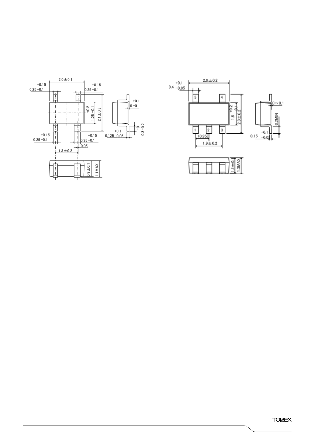
■PACKAGING INFORMATION
●USPN-4
●USPN-4 Reference Pattern Layout
0.25 0.25
4
1
0.125 0.55 0.125
3
2
Unit:mm
●USPN-4 Reference Metal Mask Design
0.2 0.2
0.55
3
0.450.4
2
4
C
0.
05
1
0.1 0.1
18/24
■PACKAGING INFORMATION (Continued)
●SSOT-24
XC6127
Series
Unit:mm
●SOT-25
19/24

XC6127 Series
■MARKING RULE
●USPN-4
① represents product series and output configuration.
MARK OUTPUT CONFIGURATION PRODUCT SERIES
F CMOS XC6127C*****-G
H Nch XC6127N*****-G
② represents detect voltage.
MARK
A
B
C
D
E
F 2.5
H
③ represents detect voltage range and release delay time / detect logic.
MARK
④ represents production lot number
0 to 9, A to Z, and inverted 0 to 9, A to Z repeated. (G, I, J, O, Q, W excepted.)
* No character inversion used.
OUTPUT VOLTAGE(V)
1.5 1.6
1.7 1.8
1.9 2.0
2.1 2.2
2.3 2.4
2.6
2.7 2.8
DETECT
VOLTAGE [V]
A 50ms/Low
B 100ms/Low
C 200ms/Low
D 400ms/Low
E 800ms/Low
F 50ms/High
H 100ms/High
K 200ms/High
L 400ms/High
M
N 50ms/Low
P 100ms/Low
R 200ms/Low
S 400ms/Low
T 800ms/Low
U 50ms/High
V 100ms/High
X 200ms/High
Y 400ms/High
Z
Odd
number
Even
number
MARK OUTPUT VOLTAGE(V) MARK OUTPUT VOLTAGE(V)
K 2.9
L
M
N
P
R
S
RELEASE DELAY TIME/
DETECT LOGIC
800ms/High
800ms/High
3.1 3.2 U 4.5 4.6
3.3 3.4 V 4.7 4.8
3.5
3.7 3.8 Y 5.1 5.2
3.9 4.0 Z 5.3 5.4
4.1
3.0 T 4.3 4.4
3.6
4.2
X 4.9 5.0
0 5.5 -
XC6127*15A**-G ~ XC6127*55A**-G
XC6127*15B**-G ~ XC6127*55B**-G
XC6127*15C**-G ~ XC6127*55C**-G
XC6127*15D**-G ~ XC6127*55D**-G
XC6127*15E**-G ~ XC6127*55E**-G
XC6127*15F**-G ~ XC6127*55F**-G
XC6127*15G**-G ~ XC6127*55G**-G
XC6127*15H**-G ~ XC6127*55H**-G
XC6127*15J**-G ~ XC6127*55J**-G
XC6127*15K**-G ~ XC6127*55K**-G
XC6127*16A**-G ~ XC6127*54A**-G
XC6127*16B**-G ~ XC6127*54B**-G
XC6127*16C**-G ~ XC6127*54C**-G
XC6127*16D**-G ~ XC6127*54D**-G
XC6127*16E**-G ~ XC6127*54E**-G
XC6127*16F**-G ~ XC6127*54F**-G
XC6127*16G**-G ~ XC6127*54G**-G
XC6127*16H**-G ~ XC6127*54H**-G
XC6127*16J**-G ~ XC6127*54J**-G
XC6127*16K**-G ~ XC6127*54K**-G
PRODUCT SERIES
20/24

)
■MARKING RULE (Continued
●SSOT-24
SSOT-24
SSOT24(方向上バー付きタイプ)
(With the orientation bar at the top)
4
3
SSOT-24
SSOT24(方向下バー付きタイプ)
(With the orientation bar at the bottom)
4
3
②①
④
③
②①
④
③
1
2
①-1 represents product series and detect voltage range, output configuration.
MARK
5
6
7
8 400ms/Low
9
A
B
C
D 400ms/High
E
F 50ms/Low
H 100ms/Low
K 200ms/Low
N 400ms/Low
P 800ms/Low
R 50ms/High
S 100ms/High
T 200ms/High
U 400ms/High
V
OUTPUT
CONFIGURATION
CMOS
DETECT
VOLTAGE [V]
number
number
* The products of CMOS output configuration are shipped in the package having the orientation bar marked in the top.
Odd
Even
1
2
RELEASE DELAY TIME/
DETECT LOGIC
50ms/Low
100ms/Low
200ms/Low
800ms/Low
50ms/High
100ms/High
200ms/High
800ms/High
800ms/High
PRODUCT SERIES
XC6127C15A**-G ~ XC6127C55A**-G
XC6127C15B**-G ~ XC6127C55B**-G
XC6127C15C**-G ~ XC6127C55C**-G
XC6127C15D**-G ~ XC6127C55D**-G
XC6127C15E**-G ~ XC6127C55E**-G
XC6127C15F**-G ~ XC6127C55F**-G
XC6127C15G**-G ~ XC6127C55G**-G
XC6127C15H**-G ~ XC6127C55H**-G
XC6127C15J**-G ~ XC6127C55J**-G
XC6127C15K**-G ~ XC6127C55K**-G
XC6127C16A**-G ~ XC6127C54A**-G
XC6127C16B**-G ~ XC6127C54B**-G
XC6127C16C**-G ~ XC6127C54C**-G
XC6127C16D**-G ~ XC6127C54D**-G
XC6127C16E**-G ~ XC6127C54E**-G
XC6127C16F**-G ~ XC6127C54F**-G
XC6127C16G**-G ~ XC6127C54G**-G
XC6127C16H**-G ~ XC6127C54H**-G
XC6127C16J**-G ~ XC6127C54J**-G
XC6127C16K**-G ~ XC6127C54K**-G
XC6127
Series
21/24

)
XC6127 Series
■MARKING RULE (Continued
①-2 represents product series and detect voltage range, output configuration.
MARK
0
1
2 200ms/Low XC6127N15C**-G ~ XC6127N55C**-G
3 400ms/Low XC6127N15D**-G ~ XC6127N55D**-G
4 800ms/Low XC6127N15E**-G ~ XC6127N55E**-G
5
6
7 200ms/High XC6127N15H**-G ~ XC6127N55H**-G
8 400ms/High XC6127N15J**-G ~ XC6127N55J**-G
9
A 50ms/Low XC6127N16A**-G ~ XC6127N54A**-G
OUTPUT
CONFIGURATION
Nch
B 100ms/Low XC6127N16B**-G ~ XC6127N54B**-G
C 200ms/Low XC6127N16C**-G ~ XC6127N54C**-G
D 400ms/Low XC6127N16D**-G ~ XC6127N54D**-G
E 800ms/Low XC6127N16E**-G ~ XC6127N54E**-G
F 50ms/High XC6127N16F**-G ~ XC6127N54F**-G
H 100ms/High XC6127N16G**-G ~ XC6127N54G**-G
K 200ms/High XC6127N16H**-G ~ XC6127N54H**-G
L 400ms/High XC6127N16J**-G ~ XC6127N54J**-G
M
* The products of Nch output configuration are shipped in the package having the orientation bar marked in the bottom.
② represents detect voltage.
MARK
A
B
C
D
E
F 2.5
H
OUTPUT VOLTAGE(V)
1.5 1.6
1.7 1.8
1.9 2.0
2.1 2.2
2.3 2.4
2.6
2.7 2.8
③④ represents production lot number. 01~09, 0A~0Z, 11~9Z, A1~A9, AA~AZ、B1~ZZ repeated.
(G, I, J, O, Q, W excluded.)
* No character inversion used.
DETECT
VOLTAGE [V]
RELEASE DELAY TIME/
DETECT LOGIC
PRODUCT SERIES
50ms/Low XC6127N15A**-G ~ XC6127N55A**-G
100ms/Low XC6127N15B**-G ~ XC6127N55B**-G
Odd
number
50ms/High XC6127N15F**-G ~ XC6127N55F**-G
100ms/High XC6127N15G**-G ~ XC6127N55G**-G
800ms/High XC6127N15K**-G ~ XC6127N55K**-G
Even
number
800ms/High XC6127N16K**-G ~ XC6127N54K**-G
MARK OUTPUT VOLTAGE(V) MARK OUTPUT VOLTAGE(V)
K 2.9
L
M
N
P
R
S
3.1 3.2 U 4.5 4.6
3.3 3.4 V 4.7 4.8
3.5
3.7 3.8 Y 5.1 5.2
3.9 4.0 Z 5.3 5.4
4.1
3.0 T 4.3 4.4
3.6
4.2
X 4.9 5.0
0 5.5 -
22/24

)
■MARKING RULE (Continued
●SOT-25
XC6127
Series
SOT-25(Under dot)
4
① ② ③ ④ ⑤
① represents product series and output configuration.
MARK OUTPUT CONFIGURATION PRODUCT SERIES
5 CMOS XC6127C*****-G
6 Nch XC6127N*****-G
* SOT-25 with the under-dot marking is used.
12
Magnified
拡大
② represents detect voltage.
MARK
A
B
C
D
E
F 2.5
H
OUTPUT VOLTAGE(V)
1.5 1.6
1.7 1.8
1.9 2.0
2.1 2.2
2.3 2.4
2.6
2.7 2.8
MARK OUTPUT VOLTAGE(V) MARK OUTPUT VOLTAGE(V)
K 2.9
L
M
N
P
R
S
3.1 3.2 U 4.5 4.6
3.3 3.4 V 4.7 4.8
3.5
3.7 3.8 Y 5.1 5.2
3.9 4.0 Z 5.3 5.4
4.1
3.0 T 4.3 4.4
3.6
4.2
X 4.9 5.0
0 5.5 -
③ represents detect voltage range and release delay time / detect logic.
MARK
A 50ms/Low
B 100ms/Low
C 200ms/Low
D 400ms/Low
E 800ms/Low
F 50ms/High
H 100ms/High
K 200ms/High
L 400ms/High
M
N 50ms/Low
P 100ms/Low
R 200ms/Low
S 400ms/Low
T 800ms/Low
U 50ms/High
V 100ms/High
X 200ms/High
Y 400ms/High
Z
DETECT
VOLTAGE [V]
Odd
number
Even
number
RELEASE DELAY TIME/
DETECT LOGIC
800ms/High
800ms/High
PRODUCT SERIES
XC6127*15A**-G ~ XC6127*55A**-G
XC6127*15B**-G ~ XC6127*55B**-G
XC6127*15C**-G ~ XC6127*55C**-G
XC6127*15D**-G ~ XC6127*55D**-G
XC6127*15E**-G ~ XC6127*55E**-G
XC6127*15F**-G ~ XC6127*55F**-G
XC6127*15G**-G ~ XC6127*55G**-G
XC6127*15H**-G ~ XC6127*55H**-G
XC6127*15J**-G ~ XC6127*55J**-G
XC6127*15K**-G ~ XC6127*55K**-G
XC6127*16A**-G ~ XC6127*54A**-G
XC6127*16B**-G ~ XC6127*54B**-G
XC6127*16C**-G ~ XC6127*54C**-G
XC6127*16D**-G ~ XC6127*54D**-G
XC6127*16E**-G ~ XC6127*54E**-G
XC6127*16F**-G ~ XC6127*54F**-G
XC6127*16G**-G ~ XC6127*54G**-G
XC6127*16H**-G ~ XC6127*54H**-G
XC6127*16J**-G ~ XC6127*54J**-G
XC6127*16K**-G ~ XC6127*54K**-G
③④ represents production lot number. 01~09, 0A~0Z, 11~9Z, A1~A9, AA~AZ、B1~ZZ repeated.
(G, I, J, O, Q, W excluded.)
23/24

XC6127 Series
* No character inversion used.
24/24
1. The products and product specifications contained herein are subject to change without
notice to improve performance characteristics. Consult us, or our representatives
before use, to confirm that the information in this datasheet is up to date.
2. We assume no responsibility for any infringement of patents, patent rights, or other
rights arising from the use of any information and circuitry in this datasheet.
3. Please ensure suitable shipping controls (including fail-safe designs and aging
protection) are in force for equipment employing products listed in this datasheet.
4. The products in this datasheet are not developed, designed, or approved for use with
such equipment whose failure of malfunction can be reasonably expected to directly
endanger the life of, or cause significant injury to, the user.
(e.g. Atomic energy; aerospace; transport; combustion and associated safety
equipment thereof.)
5. Please use the products listed in this datasheet within the specified ranges.
Should you wish to use the products under conditions exceeding the specifications,
please consult us or our representatives.
6. We assume no responsibility for damage or loss due to abnormal use.
7. All rights reserved. No part of this datasheet may be copied or reproduced without the
prior permission of TOREX SEMICONDUCTOR LTD.
 Loading...