

C
C
X
6121/X
6122
XC6123/XC6124
Series
ETR0209-011
Voltage Detector with Watchdog Function and ON/OFF Control (VDF=1.6V~5.0V)
■GENERAL DESCRIPTION
The XC6121/XC6122/XC6123/XC6124 series is a group of high-precision, low current consumption voltage detectors with
watchdog functions incorporating CMOS process technology. The series consist of a reference voltage source, delay circuit,
comparator, and output driver. With the built-in delay circuit, the series do not require any external components to output
signals with release delay time. The output type is V
watchdog functions. By setting the EN/ENB pin to low or high level, the watchdog function can be OFF while the voltage
detector remains operation. Since the EN/ENB pin of the XC6122 and XC6124 series is internally pulled up to the V
pulled down to the V
detect voltages are internally fixed 1.6V ~ 5.0V in increments of 0.1V, using laser trimming technology. Six watchdog timeout
periods are available in a range from 50ms to 1.6s. Five release delay times are available in a range from 3.13ms to 400ms.
■APPLICATIONS
●Microprocessor watchdog monitoring
and reset circuits
●Memory battery backup circuits
●System power-on reset circuits
●Power failure detection
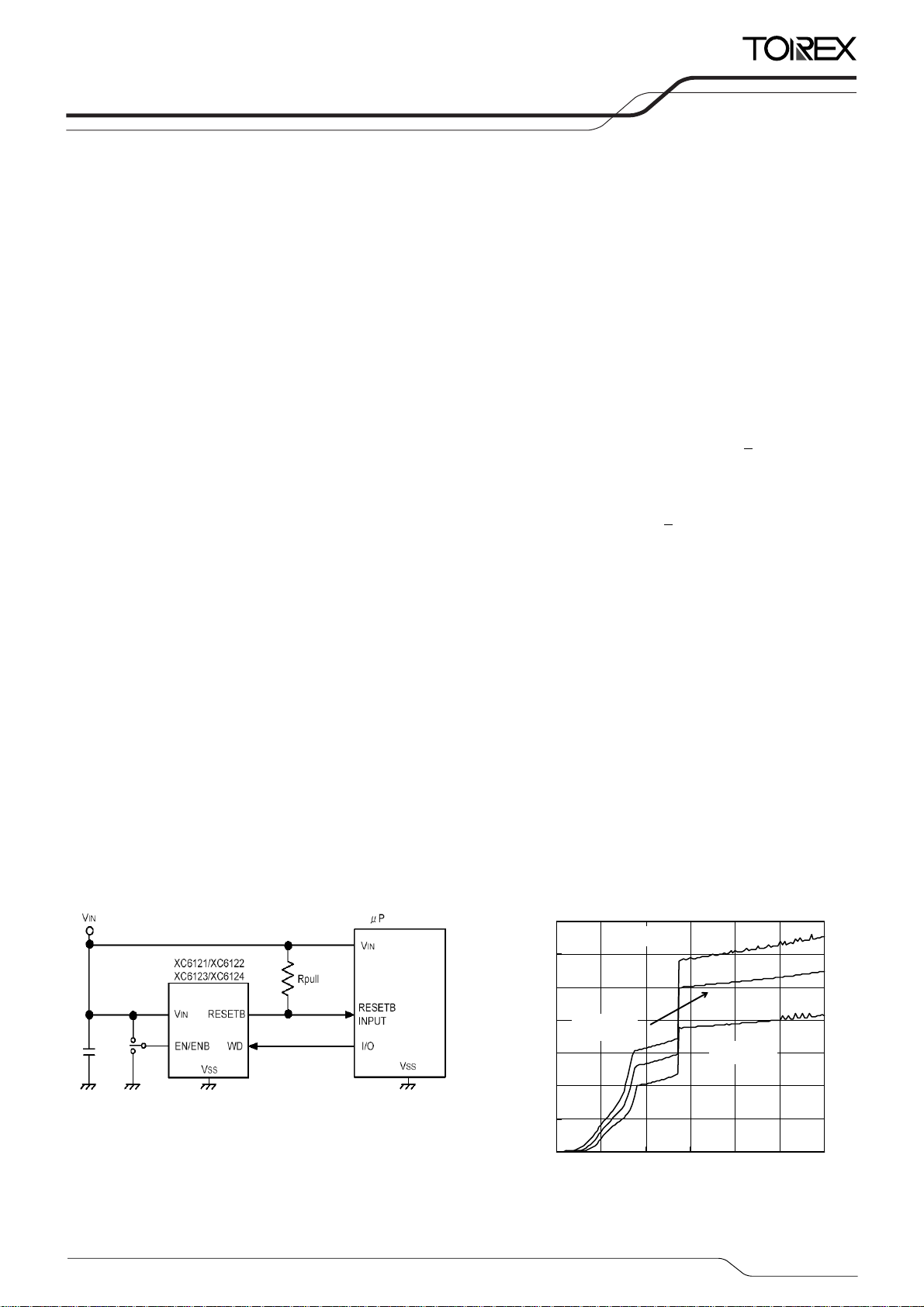
■TYPICAL APPLICATION CIRCUIT
pin, these series can be used with the EN/ENB pin left open when the watchdog functions is used. The
SS
DFL low when detected. The EN/ENB pin can control ON and OFF of the
IN pin or
■FEATURES
Detect Voltage Range : 1.6V ~ 5.0V, +2%
Hysteresis Width : VDFL x 5% (TYP.)
Operating Voltage Range : 1.0V ~ 6.0V
Detect Voltage Temperature
Characteristics
Output Configuration : N-channel open drain
Watchdog Pin : Watchdog input
EN/ENB Pin : When the EN/ENB pin voltage is
Release Delay Time : 400ms, 200ms, 100ms, 50ms,
Watchdog Timeout Period : 1.6s, 800ms, 400ms, 200ms,
Operating Ambient Tempera ture
Packages
Environmentally Friendly
(0.1V increments)
: +
100ppm/OC (TYP.)
If watchdog input maintains ‘H’ or
‘L’ within the watchdog timeout
period, a reset signal is output
from the RESETB pin.
set to low or high level, the
watchdog function is forced off.
3.13ms (TYP.)
100ms, 50ms (TYP.)
:
-40℃~ +85℃
: SOT-25, USP-6C
: EU RoHS Compliant, Pb Free
■TYPICAL PERFORMANCE
CHARACTERISTICS
●Supply Current vs. Input Voltage
XC6121~XC6124(VDF=2.7V)
14.0
12.0
10.0
(μA)
SS
8.0
6.0
4.0
Supply Current: I
2.0
Ta=25℃
0
0123456
Ta=85℃
Input V oltage: V
Ta=-40℃
(V)
IN
1/26

XC6121/XC6122/XC6123/XC6124
■PIN CONFIGURATION
■PIN ASSIGNMENT
PIN NUMBER
SOT-25 USP-6C
1 4
2 5
3 2 EN/ENB Watchdog ON/OFF Control
4 1 WD Watchdog
5 6 VIN Power Input
- 3 NC No Connection
2/26
SOT-25
(TOP VIEW)
PIN NAME FUNCTION
RESETB Reset Output
V
Ground
SS
Series
USP-6C
(BOTTOM VIEW)
* The dissipation pad for the USP-6C package should be
solder-plated in reference mount pattern and metal masking
so as to enhance mounting strength and heat release. If
the pad needs to be connected to other pins, it should be
connected to the V
SS (No. 5) pin.
XC6121/XC6122/XC6123/XC6124
■PRODUCT CLASSIFICATION
●Selection Guide
RESET OUTPUT EN/ENB PIN FUNCTION
SERIES
VDFL (RESETB)
(*1)
VDFH (RESET)
XC6121 N-channel open drain - EN
XC6122 N-channel open drain - EN
XC6123 N-channel open drain - ENB
XC6124 N-channel open drain -
(*1)
The output type of RESETB is set to L level at the time of detection.
(*2)
EN input logic: The watchdog function turns on when the EN pin becomes high level.
ENB input logic: The watchdog function turns on when the ENB pin becomes low level.
●Ordering Information
XC6121①②③④⑤⑥-⑦
XC6122①②③④⑤⑥-⑦
XC6123①②③④⑤⑥-⑦
XC6124①②③④⑤⑥-⑦
(*2)
: N-channel Open Drain Output (RESETB), EN Pin: No Pull-Up Resistor
(*2)
: N-channel Open Drain Output (RESETB), EN Pin: Pull-Up Resistor
(*2)
: N-channel Open Drain Output (RESETB), ENB Pin: No Pull-Down Resistor
(*2)
: N-channel Open Drain Output (RESETB), ENB Pin: Pull-Down Resistor
DESIGNATOR ITEM SYMBOL DESCRIPTION
① Release Delay Time
(*1)
② Watchdog Timeout Period
③④ Detect Voltage 16 ~ 50
⑤⑥-⑦
(*1)
Please set the release delay time shorter than or equal to the watchdog timeout period.
ex.) XC6121D327MR or XC6121D627MR
(*2)
The “-G” suffix denotes Halogen and Antimony free as well as being fully RoHS compliant.
(*2)
Packages
(Order Unit)
HYSTERESIS
EN/ENB Input
Logic
Available:
x 5% (TYP.)
V
DFL
ENB
A 3.13ms (TYP.)
C 50ms (TYP.)
D 100ms (TYP.)
E 200ms (TYP.)
F 400ms (TYP.)
2 50ms (TYP.)
3 100ms (TYP.)
4 200ms (TYP.)
5 400ms (TYP.)
6 1.6s (TYP.)
7 800ms (TYP.)
Detect voltage
ex.) 4.5V: ③⇒4, ④⇒5
MR SOT-25 (3,000/Reel)
MR-G SOT-25 (3,000/Reel)
ER USP-6C (3,000/Reel)
ER-G USP-6C (3,000/Reel)
(*2)
Series
Pull-Up or Down
Resistor
With No Pull-Up
Resistor
With Pull-Up
Resistor
With No Pull-Down
Resistor
With Pull-Down
Resistor
3/26
XC6121/XC6122/XC6123/XC6124
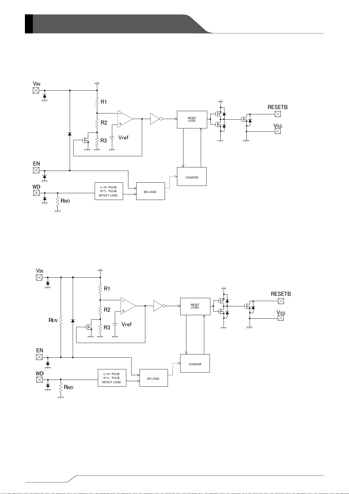
■BLOCK DIAGRAMS
●XC6121 Series
●XC6122 Series
4/26
Series
N-ch Open Drain Output
N-ch Open Drain Output
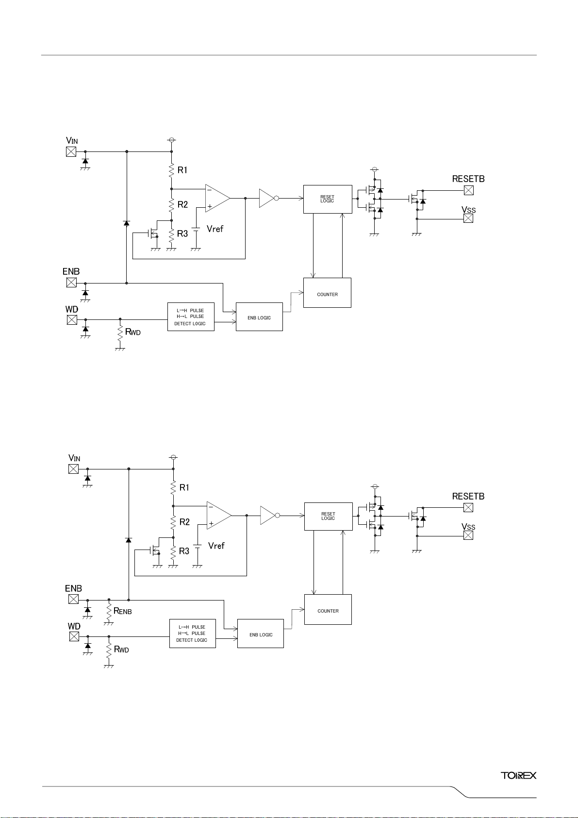
■BLOCK DIAGRAMS (Continued)
●XC6123 Series
●XC6124 Series
XC6121/XC6122/XC6123/XC6124
Series
N-ch Open Drain Output
N-ch Open Drain Output
5/26
XC6121/XC6122/XC6123/XC6124
■ABSOLUTE MAXIMUM RATINGS
PAR AMET ER SYMBOL RATINGS UNITS
VIN VSS -0.3 ~ 7.0 V
Power Dissipation
6/26
Input Voltage
Output Current I
Output Voltage V
SOT-25 250
USP-6C
Operating Ambient Temperature Topr -40 ~ +85
Storage Temperature Tstg -55 ~ +125
VEN/V
V
RBOUT
RESETB
Pd
WD
Series
Ta =2 5OC
V
ENB
SS-0.3~VIN+0.3≦7.0
V
VSS -0.3 ~ 7.0 V
20 mA
SS -0.3 ~ 7.0
V
120
V
mW
O
C
O
C
XC6121/XC6122/XC6123/XC6124
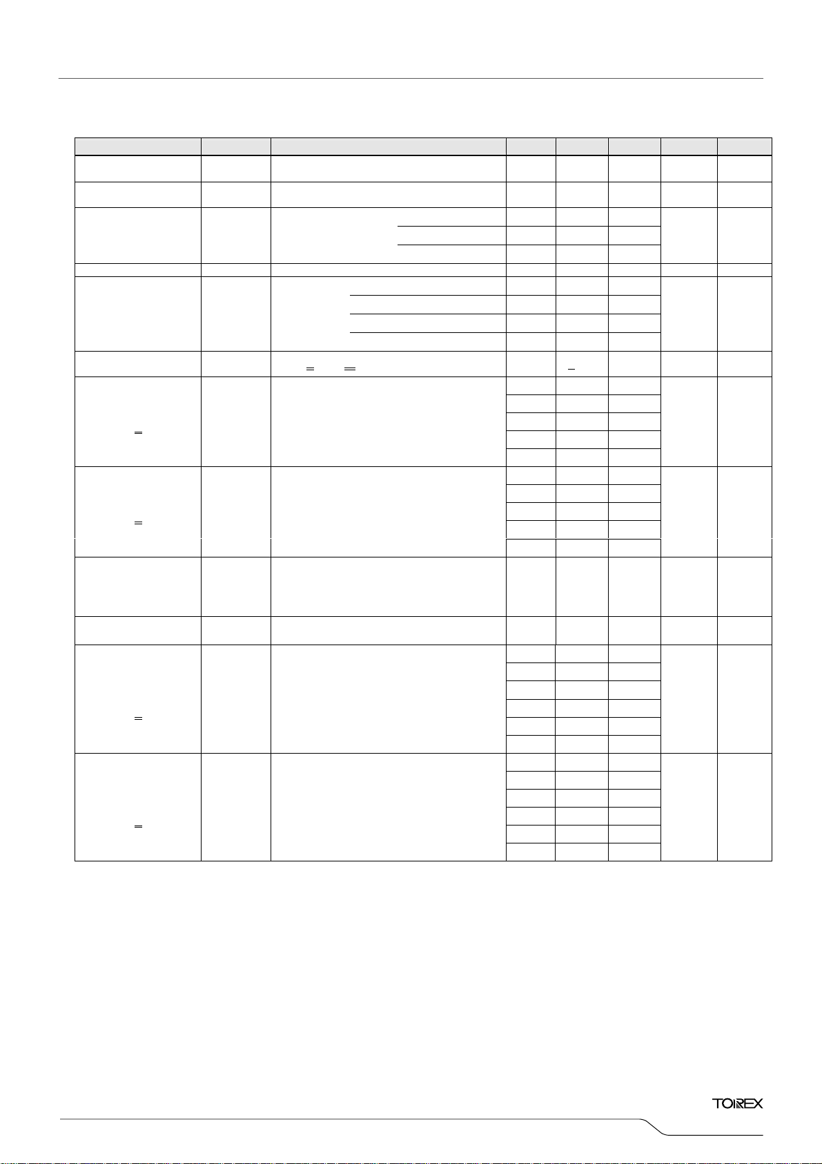
■ELECTRICAL CHARACTERISTICS
PAR AMET ER SYMBOL CONDITIONS MIN. TYP. MAX. UNITS CIRCUIT
DFL(T)
Detect Voltage VDFL
V
EN
=VSS
Hysteresis Width VHYS VEN=VSS
Supply Current
(*1)
ISS WD=OPEN
VIN=V
VIN=V
×0.9V - 5 11
DFL(T)
×1.1V - 10 16
DFL(T)
=6.0V - 12 18
V
IN
V
× 0.98
VDFL
× 0.02
VDFL(T)
VDFL
× 0.05
Operating Voltage VIN 1.0 - 6.0 V ①
VIN=1.0V 0.15 0.5 -
Output Current IRBOUT
Temperature
Characteristics
△VDFL /
△Topr・VDFL
N-ch.
VDS=0.5V
-40OC < Topr < 85
VIN=2.0V (VDFL(T)> 2.0V) 2.0 2.5 -
VIN=3.0V (VDFL(T) >3.0V) 3.0 3.5 -
V
IN=4.0V (VDFL(T) >4.0V) 3.5 4.0 -
O
C - +100 - ppm/
2.00 3.13 5.00
Release Delay Time
(VDFL<1.8V)
tDR
Time until VIN is increased from
1.0V to 2.0V
and attains to the release time level,
and the Reset output pin releases.
37 50 63
75 100 125
150 200 250
300 400 500
2.00 3.13 5.00
Release Delay Time
(VDFL>1.9V)
tDR
Time until VIN is increased from
1.0V to (VDFL x 1.1V)
and attains to the release time level,
and the Reset output pin releases.
37 50 63
75 100 125
150 200 250
300 400 500
Time until VIN is decreased from 6.0V to
Detect Delay Time tDF
1.0V and attains to the detect voltage
level, and the Reset output pin detects
- 5.5 33 μs ④
while the WD pin left open.
VDFL
Leakage Current
LEAK VIN=6.0V, V
I
=6.0V - 0.01 0.1 μA ③
RESETB
37 50 63
Watchdog
Timeout Period
(V
DFL<1.8V)
t
WD
Time until V
1.0V to 2.0V and
the Reset output pin is released to go
IN increases form
into the detection state. (WD=OPEN)
75 100 125
150 200 250
300 400 500
600 800 1000
1200 1600 2000
37 50 63
Watchdog
Timeout Period
(V
DFL>1.9V)
t
WD
Time until V
1.0V to (V
and the Reset output pin is released to
IN increases from
DFLx1.1V)
go into the detection state. (WD=OPEN)
75 100 125
150 200 250
300 400 500
600 800 1000
1200 1600 2000
VDFL(T)
× 1.02
VDFL
× 0.08
μA ②
mA ③
ms ④
ms ④
ms ⑤
ms ⑤
Series
Ta =2 5OC
V ①
V ①
O
C ①
7/26

XC6121/XC6122/XC6123/XC6124
■ELECTRICAL CHARACTERISTICS (Continued)
Series
PAR AMET ER SYMBOL CONDITIONS MIN. TYP. MAX. UNITS CIRCUIT
V
Watchdog
Minimum Pulse Width
Watchdog
High Level Voltage
Watchdog
Low Level Voltage
Watchdog
Pull-down Resistance
EN/ENB
High Level Voltage
EN/ENB
Low Level Voltage
EN Pull-up
Resistance
ENB Pull-down
Resistance
NOTE:
* In case where no EN/ENB pin’s condition written in the test condition field, V
** V
DFL(T)
(*1)
The condition when the watchdog pin is ON.
The EN/ENB pin is CMOS input. For the XC6122 (pull-up resistor) and XC6124 (pull-down resistor),
supply current increases in the following values when the watchdog function is OFF.
XC6122 Series:(V
XC6124 Series:V
(*2)
For the XC6122 series only.
(*3)
For the XC6124 series only.
(*2)
(*3)
=Setting detect voltage value
t
WDIN
V
WDH VIN=VDFL x 1.1V ~ 6.0V VIN x 0.7 - 6 V ⑥
VWDL VIN=VDFL x 1.1V ~ 6.0V 0 - VIN x 0.3 V ⑥
RWD
V
ENH/VENBH VIN=VDFL x 1.1V ~ 6.0V 1.3 - VIN V ⑧
V
ENL/VENBL VIN=VDFL x 1.1V ~ 6.0V 0 - 0.35 V ⑧
EN VIN=6.0V, V
R
ENB VIN=6.0V, V
R
IN-VEHL)/1.6MΩ(TYP.)
EHBH/1.6MΩ(TYP.)
IN=6.0V,
Apply pulse from 6.0V to 0V to the WD
pin.
VWD=6V, RWD=VWD/IWD
=0V, REN=VIN / IEN
EN
=6V, RENB=VENB / IENB
ENB
EN=VIN
300 - - ns ⑥
300
600 900 kΩ ⑦
1.0 1.6 2.4 MΩ ⑨
and V
ENB=VSS
.
Ta =2 5OC
8/26
 Loading...