

p
)
XC6120 Series
ETR0209-009
Highly Accurate, Ultra Small, Low Power Consumption Voltage Detector
■GENERAL DESCRIPTION
The XC6120 series are highly precise, low power consumption voltage detectors, manufactured using CMOS and laser
trimming technologies. With low power consumption and high accuracy, the series is suitable for precision mobile equipment.
The XC6120 in ultra small packages are ideally suited for high-density mounting. The XC6120 is available in both CMOS and
N-channel open drain output configurations.
■APPLICATIONS
●Microprocessor reset circuitry
●Memory battery back-up circuits
●Power-on reset circuits
●Power failure detection
●System battery life and charge voltage monitors
■TYPICAL APPLICATION CIRCUIT
(Unused for the CMOS
out
ut products
■FEATURES
Highly Accurate : ± 2% (VDF≧1.5V)
: ± 30mV (V
Low Power Consumption : 0.6μA [V
Detect Voltage Range : 1.0V ~ 5.0V (0.1V increments)
Operating Voltage Range : 0.7V ~ 6.0V
Detect Voltage T emperature Characteristics
: ±100ppm/℃ (TYP.)
Output Configuration : CMOS (XC6120C)
: N-channel open drain (XC6120N)
Operating
Temperature Range : -40℃~85℃
Packages : USP-3, SSOT-24
Environmentally Friendly : EU RoHS Compliant, Pb Free
<1.5V)
DF
=2.7V, VIN=2.97V]
DF
■ TYPICAL PERFORMANCE
CHARACTERISTICS
●Supply Current vs. Input Voltage
XC6120x272xx
3.5
3.0
2.5
(μA)
SS
2.0
1.5
1.0
Supply Current: ISS (μA)
Supply Current: I
0.5
0.0
0123456
Input Voltage: VIN (V)
Ta= 85℃
25℃
-40℃
1/13

XC6120 Series
■PIN CONFIGURATION
■PIN ASSIGNMENT
V
OUT
USP-3
(BOTTOM VIEW)
VSS
VIN
PIN NUMBER
USP-3 SSOT-24
PIN NAME FUNCTION
VIN
NC
SSOT-24
(TOP VIEW)
1 4 VIN Power Input
3 2 VSS Ground
2 3 V
Output (Detect ”Low” )
OUT
- 1 NC No Connection
■PRODUCT CLASSIFICATION
●Ordering Information
XC6120①②③④⑤⑥-⑦
(*1)
DESIGNATOR ITEM SYMBOL DESCRIPTION
①
②③
④
⑤⑥-⑦
(*1)
The “-G” suffix indicates that the products are Halogen and Antimony free as well as being fully RoHS compliant.
■BLOCK DIAGRAMS
(1) XC6120C
(*1)
Output Configuration
Detect Voltage (V
Detect Accuracy 2
Packages
(Order Unit)
) 10~50
DF
V
OUT
VSS
C
N
CMOS output
N-ch open drain output
For example 1.0V → ②1, ③0
±2%
HR USP-3 (3,000/Reel)
HR-G USP-3 (3,000/Reel)
NR SSOT-24 (3,000/Reel)
NR-G SSOT-24 (3,000/Reel)
(2) XC6120N
2/13

XC6120
■ABSOLUTE MAXIMUM RATINGS
PAR AMETER SYMBOL RATING UNITS
V
-0.3~7.0
SS
-0.3~7.0
V
SS
150
-40~+85
-55~+125
Output Voltage
Power Dissipation
Input Voltage
Output Current I
CMOS Output VSS-0.3~VIN+0.3
N-ch Open Drain Output
USP-3 120
SSOT-24
V
V
OUT
OUT
Pd
IN
Operating Temperature Range Topr
Storage Temperature Range Tstg
10 mA
■ELECTRICAL CHARACTERISTICS
XC6120 Series
PAR AMETER SYMBOL CONDITION MIN. TYP. MAX. UNITS CIRCUIT
Operating Voltage VIN V
=1.0~5.0V
DF(T)
(*1)
0.7 - 6.0 V -
Ta =2 5 ℃
V
V
mW
℃
℃
Series
Ta =2 5 ℃
Detect Voltage VDF V
Hysteresis Width V
Supply Current 1 I
Supply Current 2 I
V
HYS
V
SS1
V
SS2
=1.0V~5.0V E-1 V ①
DF(T)
=1.0V~5.0V
DF(T)
IN=VDF(T)
= V
IN
×1.1 E-2 μA ②
×0.9V E-3 μA ②
DF(T)
V
VIN=0.7V
V
V
I
I
OUTP
OUTN
I
LEAK
(*2)
Output Current
Leakage
Current
Output(Pch)
N-ch Open
CMOS
Drain
ΔV
Temperature
Characteristics
Detect Delay Time
Release Delay Time
*1: VDF (T): Nominal detect voltage
*2: For XC6120C only.
*3: A time taking from the time at VIN = VDF to the time at V
*4: V
: Release voltage (VDR = VDF + V
DR
*5: A time taking from the time at V
●XC6120N recommended pull-up resistance
(*3)
t
(*5)
t
DF
(ΔTopr・
V
)
DF
DF
DR
VIN=1.0V V
VIN=2.0V V
VIN=3.0V V
V
=4.0V V
IN
OUT
OUT
OUT
OUT
VIN=6.0V V
VIN=VDF×0.9V, V
=6.0V, V
V
IN
/
HYS
= VDR to the time at V
IN
o
C≦Topr≦85 oC - ±100 - ppm/oC ①
-40
V
=6.0V→0.7V
IN
V
V
IN=VDF
V
=0.7V→6.0V
IN
IN=VDR
to V
to V
)
=0.1V, V
=0.1V, V
=0.1V, V
=0.1V, V
OUT
OUT
OUT=VDR
OUT
OUT
Input Voltage Range Pull-up Resistance
0.7V~6.0V
0.8V~6.0V
1.0V~6.0V
≧ 220kΩ
≧ 100kΩ
≧ 33kΩ
V
V
DF
×
0.03
=0.5V 0.09 0.57 -
OUT
=0.3V 0.08 0.56 -
OUT
=0.1V 0.05 0.30 -
OUT
>1.0V 0.46 0.71 -
DF(T)
>2.0V 1.15 1.41 -
DF(T)
>3.0V 1.44 1.77 -
DF(T)
>4.0V 1.61 1.96 -
DF(T)
=5.5V - -0.95 -0.60 mA ③
OUT
=0V - -0.001 -
OUT
DF
×
0.05
V
DF
×0.07
V ①
mA ③
μA ③
=6.0V - 0.001 0.10
=0.5V
(*4)
- 30 100 μs ④
- 20 100 μs ④
=0.5V when VIN falls from 6.0V to 0.7V.
= VDR when VIN rise from 0.7V to 6.0V.
3/13

XC6120 Series
■ELECTRICAL CHARACTERISTICS (Continued)
● DETECT VOLTAGE ACCURACY AND SUPPLY CURRENT SPECIFICATIONS
SYMBOL E-1 E-2 E-3
PARAMETER
NOMINAL DETECT
(※6 )
When detect voltage is 1.0V≦V
When detect voltage is 1.5V≦V
4/13
VOLTAGE
V
MIN. MAX. TYP. MAX. TYP. MAX.
DF(T)
1.0 0.970 1.030
1.1 1.070 1.130
1.2 1.170 1.230
1.3 1.270 1.330
1.4 1.370 1.430
1.5 1.470 1.530
1.6 1.568 1.632
1.7 1.666 1.734
1.8 1.764 1.836
1.9 1.862 1.938
2.0 1.960 2.040
2.1 2.058 2.142
2.2 2.156 2.244
2.3 2.254 2.346
2.4 2.352 2.448
2.5 2.450 2.550
2.6 2.548 2.652
2.7 2.646 2.754
2.8 2.744 2.856
2.9 2.842 2.958
3.0 2.940 3.060
3.1 3.038 3.162
3.2 3.136 3.264
3.3 3.234 3.366
3.4 3.332 3.468
3.5 3.430 3.570
3.6 3.528 3.672
3.7 3.626 3.774
3.8 3.724 3.876
3.9 3.822 3.978
4.0 3.920 4.080
4.1 4.018 4.182
4.2 4.116 4.284
4.3 4.214 4.386
4.4 4.312 4.488
4.5 4.410 4.590
4.6 4.508 4.692
4.7 4.606 4.794
4.8 4.704 4.896
4.9 4.802 4.998
5.0 4.900 5.100
DETECT VOLTAGE
VDF (V)
XC6120xxx2 Series
<1.5V, detect accuracy is ±30mV.
DF(T)
≦5.0V, detect accuracy is ±2%.
DF(T)
SUPPLY CURRENT 1
I
(μA)
SS1
0.5 1.4 0.4 1.35
0.6 1.7 0.5 1.60
0.7 1.9 0.6 1.80
SUPPLY CURRENT 2
I
(μA)
SS2

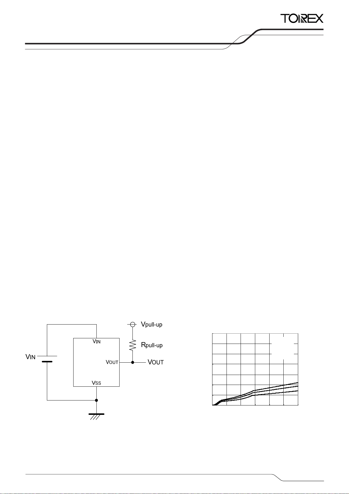
■TEST CIRCUITS
Circuit 1
Circuit 2 Circuit 3
Circuit 4
R
=100kΩ
PULL
(Unused for the CMOS output products)
=100kΩ
R
PULL
(Unused for the CMOS output products)
Measurement of waveform
XC6120
Series
5/13

XC6120 Series
■OPERATIONAL EXPLANATION
●Typical Application Circuit
VIN
●Timing Charge
The following explains the operation of the typical application circuit along number symbols shown in the timing chart.
① When input voltage (V
(A condition of high impedance exists with N-ch open drain output configurations.)
② When input voltage (VIN) falls below detect voltage (VDF), output voltage (V
(V
③ When input voltage (V
unstable. If In this condition, VIN will equal the pulled-up output (should output be pulled-up.) (Input voltage, VIN, in
the typical application circuit.)
④ When input voltage (V
(V
⑤ When the input voltage (VIN) rises above the release voltage (VDR), output voltage (V
(V
⑥ The difference between V
Input Voltage
Note: For explaining in a simplified case, an operation time of the circuit is not counted.
) level.
SS
), output keeps the ground voltage level (VSS).
DR
). (A condition of high impedance exists with N-ch open drain output configurations.)
IN
VIN
VSS
(V
IN
Output
Voltage
(V
OUT
VOUT
)
)
) is higher than detect voltage (VDF), output voltage (V
IN
) falls to a level below that of the minimum operating voltage (V
IN
) rises above the minimum operating voltage (V
IN
DR
6/13
R
PULL
(Unused for the CMOS output products)
VOUT
①② ④③ ⑤
and VDF represents the hysteresis width.
Release Voltage (VDR)
⑥
Detect Voltage (V
)
DF
Minimum Operating Voltage (V
Ground Voltage (VSS)
Ground Voltage (V
) will be equal to input voltage (VIN).
OUT
) will be equal to the ground voltage
OUT
), output will become
MIN
) level until it achieves a release voltage
MIN
will be equal to input voltage
OUT
SS
)
MIN
)

XC6120
Series
■NOTE ON USE
1. Please use this IC within the stated maximum ratings. For temporary, transitional voltage drop or voltage rising
phenomenon, the IC is liable to malfunction should the ratings be exceeded.
2. In order to stabilize the IC's operations, please ensure that VIN pin's input frequency's rise and fall times are more than
several μs / V.
3. With a resistor connected between the V
voltage at the detect and release voltage. Those errors are not constant because of the fluctuation of the supply current.
4. When a resistor is connected between the VIN pin and the power supply VDD, oscillation may occur as a result of through
current and voltage drop at the R
in the CMOS output configurations, oscillation may occur regardless of detect/release operation if load current (I
exists. (refer to the Oscillation Description (2) below)
5. Please use N-ch open drains configuration, when a resistor RIN is connected between the VIN pin and the power supply
6. Torex places an importance on improving our products and its reliability.
[Figure 1: Circuit connected with the input resistor]
● Oscillation Description
(1) Oscillation as a result of through current
Since the XC6120 series are CMOS ICs, transient through current will flow when the IC's internal circuit switching operates
regardless of output configuration. Consequently, oscillation is liable to occur as a result of the similar operations as in (1)
above. This oscillation does not occur during the detect operation.
(2) Output current oscillation with the CMOS output configuration
As shown in figure 2, when the voltage applied at the power supply (VDD) rises from below detect voltage to above release
voltage, the IC commence release operations and the internal P-ch driver transistor will be on. The output current (I
the input resistor (R
voltage drops R
below the V
stop because the output current (I
become the same voltage level as the input voltage (V
therefore, the release operations will begin over again. Oscillation may occur with this repetition. Further, this condition will
also appear via means of a similar mechanism during detect operations.
power source. In such cases, please ensure that RIN is less than 10kΩ and that C is more than 0.1μF.
V
DD
However, by any possibility, we would request user fail-safe design and post-aging treatment on system or equipment.
) via the P-ch driver transistor. Because of the input resistor (RIN) and the output current (I
IN
x I
IN
and detect operations will commerce so that the internal P-ch driver transistor will be off. The voltage drop will
DF
. If the voltage drop level is larger than the IC’s hysteresis width (V
OUT
[Figure 2: Oscillation caused by the input resistor of the CMOS output product and the output current]
at the time of voltage release. (refer to the Oscillation Description (1) below ) Especially
IN
) which was flowing the P-ch driver transistor will run down. The input pin voltage will
OUT
pin and the power supply VDD some errors may be observed from the input
IN
V
PULL
R
PULL
XC6120N
) flows
OUT
), an input pin
OUT
), the input pin voltage will falls
HYS
). For this, the input pin voltage will rise above the release voltage (VDR),
IN
XC6120C
OUT
7/13
)

XC6120 Series
■TYPICAL PERFORMANCE CHARACTERISTICS
(1) Supply Current vs. Input Voltage
XC6120x102xx
XC6120x502xx
3.5
3.0
2.5
(μA)
SS
2.0
1.5
1.0
Supply Curr ent: I
0.5
0.0
0123456
Ta= 85℃
25℃
-40℃
Input Voltage: VIN (V)
(2) Output Voltage vs. Input Voltage
XC6120C202xx
6
5
(V)
OUT
4
3
2
Output Voltage: V
1
0
0123456
Input Voltage: VIN (V)
Ta= 25℃
3.5
3.0
2.5
(μA)
SS
2.0
1.5
1.0
Supply Current: I
0.5
0.0
0123456
Ta= 85℃
25℃
-40℃
Input Voltage: VIN (V)
XC6120N202xx
7
6
(V)
5
OUT
4
3
2
Output Voltage: V
1
0
0.0 0.5 1.0 1.5 2.0 2.5 3.0
Ta= 85℃
Vpull-up=6V Rpull-up=100kΩ
25℃
-50℃
Input Voltage: VIN (V)
(3) Detect Voltage, Release Voltage vs. Ambient Temperature
XC6120x102xx
1.20
1.15
(V)
DF
1.10
1.05
1.00
Detect Voltage: V
0.95
0.90
-50 -25 0 25 50 75 100
DR
V
DF
V
Ambient Temperature: Ta (℃)
1.20
1.15
1.10
1.05
1.00
0.95
0.90
(V)
DR
Release Voltage: V
8/13
XC6120x202xx
2.4
2.3
(V)
DF
2.2
2.1
2.0
Detect Voltage: V
1.9
1.8
-50 -25 0 25 50 75 100
Ambient Temperature: Ta (℃)
DR
V
DF
V
2.4
2.3
2.2
2.1
2.0
1.9
1.8
(V)
DR
Release Voltage: V

■TYPICAL PERFORMANCE CHARACTERISTICS (Continued)
(4) Output Current (Nch Driver) vs. Input Voltage
XC6120
Series
XC6120x502xx
OUT
=0.5V
10
Ta= -40℃
(mA)
8
25℃
OUTN
85℃
6
4
2
V
Output Current(Nch): I
0
0123456
Input Voltage: VIN [V]
XC6120x502xx
OUT
V
(mA)
OUTN
6
5
Ta= -40℃
4
25℃
3
85℃
2
=0.1V
XC6120x502xx
OUT
V
10
Ta= -40℃
(mA)
8
25℃
OUTN
85℃
6
4
2
=0.3V
Output Current(Nch): I
0
0123456
Input Voltage: VIN (V)
(5) Output Current (Pch Driver) vs. Input Voltage
XC6120C102xx
OUT=VIN
V
-0.5V
Ta= 8 5℃
25 ℃
-40℃
(mA)
OUTP
0.00
-0.25
-0.50
-0.75
-1.00
1
Output Current(Nch): I
0
0123456
Input Voltage: VIN (V)
XC6120C102xx
OUT=VIN
V
0.00
(mA)
-0.20
OUTP
-0.40
-0.60
-0.80
Output Current(Pch): I
-1.00
123456
Input Voltage: VIN (V)
-0.3V
Ta= 85℃
25℃
-40℃
-1.25
Output Current(Pch): I
-1.50
123456
Input Voltage: VIN (V)
XC6120C102xx
OUT=VIN
0.00
-0.05
(mA)
OUTP
-0.10
-0.15
-0.20
-0.25
Output Current(Pch): I
-0.30
123456
Input Voltage: VIN (V)
V
Ta= 85℃
-0.1V
25℃
-40℃
9/13

XC6120 Series
■PACKAGING INFORMATION
●USP-3
●SSOT-24
(unit : mm)
●USP-3 Reference Pattern Layout
0.4
1.35
0.25
0.7
●USP-3 Reference Metal Mask Design
0.3
1.2
0.25
0.5
10/13

■ MARKING RULE
●SSOT-24
SSOT-24
(TOP VIEW)
① represents output configuration and detect voltage Range
② represents detect voltage
③,④ represents production lot number
XC6120
Series
MARK OUTPUT CONFIGURATION OUTPUT VOLTAGE PRODUCT SERIES
K
L
M
N
CMOS
Nch open drain
MARK DETECT VOLTAGE (V) MARK DETECT VOLTAGE (V)
0 - 3.0
1 - 3.1
2 - 3.2
3 - 3.3
4 - 3.4
5 - 3.5
6 - 3.6
7 - 3.7
8 - 3.8
9 - 3.9
A 1.0 4.0
B 1.1 4.1
C 1.2 4.2
D 1.3 4.3
E 1.4 4.4
01 to 09, 10, 11, …, 99, 0A, …, 0Z, 1A, …repeated.
(G, I, J, O, Q, W excluded. Reversed character is not used.)
1.0V~2.9V
3.0V~5.0V
1.0V~2.9V
3.0V~5.0V
F
H
K
L
M
N
P
R
S
T
U
V
X
Y
Z
XC6120C
XC6120N
1.5 4.5
1.6 4.6
1.7 4.7
1.8 4.8
1.9 4.9
2.0 5.0
2.1 -
2.2 -
2.3 -
2.4 -
2.5 -
2.6 -
2.7 -
2.8 -
2.9 -
11/13

XC6120 Series
■ MARKING RULE (Continued)
●USP-3
1
2
3
② ③①
④ ⑤
3
USP-3
(TOP VIEW)
① represents product series
MARK PRODUCT SERIES
0 XC6120******
② standard:represents output configuration and integer number of detect voltage
●CMOS Output (XC6120C Series)
MARK DETECT VOLTAGE (V)
A 1.X
B 2.X
C 3.X
D 4.X
E 5.X
③ standard:represents decimal point of detect voltage
MARK DETECT VOLTAGE (V) PRODUCT SERIES
3
0
④,⑤ represents production lot number
01 to 09, 10, 11, …, 99, 0A, …, 0Z, 1A, …repeated.
(G, I, J, O, Q, W excluded.)
X.3
X.0
●Nch open drain (XC6120N Series)
MARK DETECT VOLTAGE (V)
F 1.X
H 2.X
K 3.X
L 4.X
M 5.X
XC6120**3***
XC6120**0***
12/13

XC6120
Series
1. The products and product specifications contained herein are subject to change without
notice to improve performance characteristics. Consult us, or our representatives
before use, to confirm that the information in this datasheet is up to date.
2. We assume no responsibility for any infringement of patents, patent rights, or other
rights arising from the use of any information and circuitry in this datasheet.
3. Please ensure suitable shipping controls (including fail-safe designs and aging
protection) are in force for equipment employing products listed in this datasheet.
4. The products in this datasheet are not developed, designed, or approved for use with
such equipment whose failure of malfunction can be reasonably expected to directly
endanger the life of, or cause significant injury to, the user.
(e.g. Atomic energy; aerospace; transport; combustion and associated safety
equipment thereof.)
5. Please use the products listed in this datasheet within the specified ranges.
Should you wish to use the products under conditions exceeding the specifications,
please consult us or our representatives.
6. We assume no responsibility for damage or loss due to abnormal use.
7. All rights reserved. No part of this datasheet may be copied or reproduced without the
prior permission of TOREX SEMICONDUCTOR LTD.
13/13
 Loading...