

r
XC6101~XC6105, XC6111~XC6117
Series
ETR0207_016
Voltage Detector (VDF=1.6V~5.0V)
■GENERAL DESCRIPTION
The XC6101~XC6105, XC6111~XC6117 series are groups of high-precision, low current consumption voltage detectors with
manual reset input and watchdog functions incorporating CMOS process technology. The series consist of a reference
voltage source, delay circuit, comparator, and output driver. With the built-in delay circuit, the XC6101 ~ XC6105, XC6111 ~
XC6117 series do not require any external components to output signals with release delay time. Moreover, with the manual
reset function, reset can be asserted at any time. The ICs produce two types of output; V
(high when detected). With the XC6101 ~ XC6105, XC6111 ~ XC6115 series, the WD pin can be left open if the watchdog
function is not used. Whenever the watchdog pin is opened, the internal counter clears before the watchdog timeout occurs.
Since the manual reset pin is internally pulled up to the V
pin unconnected if the pin is unused. The detect voltages are internally fixed 1.6V ~ 5.0V in increments of 0.1V, using laser
trimming technology. Six watchdog timeout periods are available in a range from 6.25ms to 1.6s. Seven release delay times
are available in a range from 3.13ms to 1.6s.
■APPLICATIONS
●Microprocessor reset circuits
●Memory battery backup circuits
●System power-on reset circuits
●Power failure detection
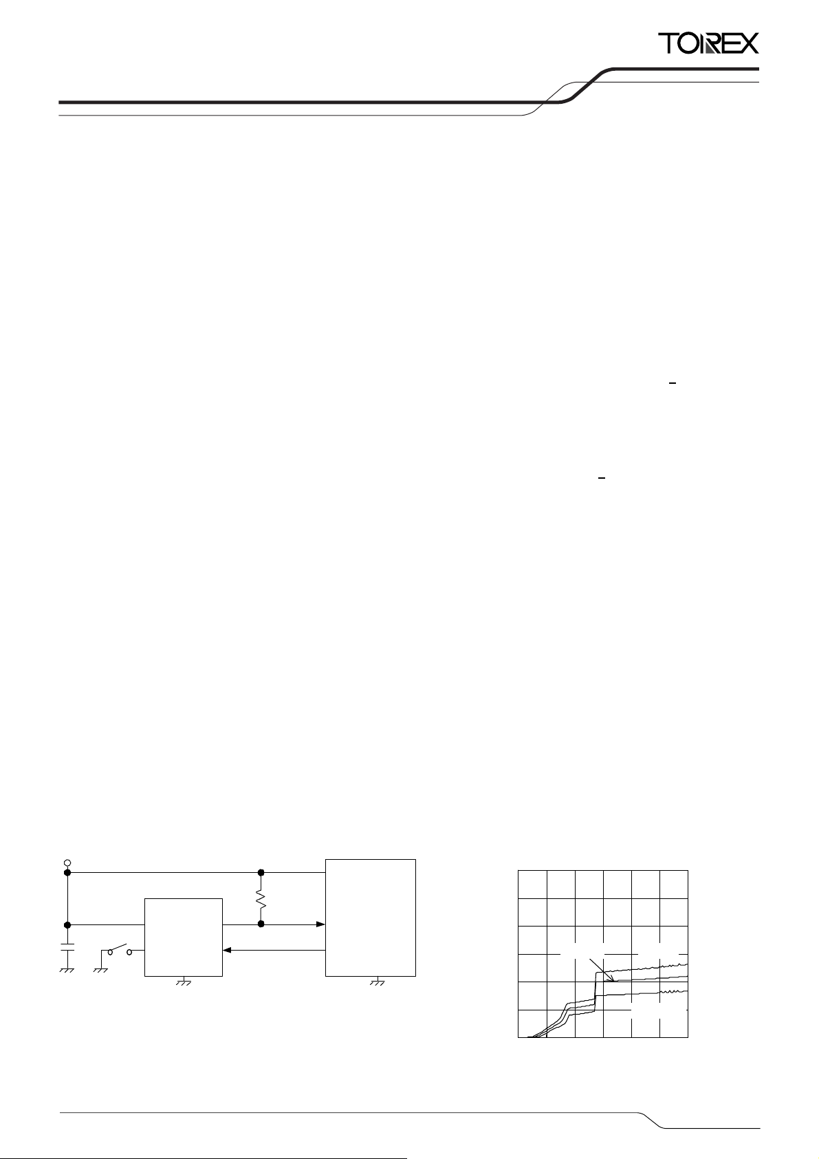
■TYPICAL APPLICATION CIRCUIT
VIN
* Not necessary with CMOS output products.
XC6101/XC6102
VIN
MRB
VSS
RESETB
WD
Rpull
*
VIN
RESETB
INPUT
I/O
IN pin voltage level, the ICs can be used by leaving the manual reset
■FEATURES
Detect Voltage Range : 1.6V ~ 5.0V, +2%
Hysteresis Width : V
V
Operating Voltage Range : 1.0V ~ 6.0V
Detect Voltage Temperature
Coefficient
Output Configuration : N-channel open drain,
Reset Output Options : V
Watchdog Function : Watchdog input WD;
Manual Reset Function : Manual Reset Input MRB;
Release Delay Time : 1.6s, 400ms, 200ms, 100ms,
Watchdog Timeout Period : 1.6s, 400ms, 200ms, 100ms,
Operating Ambient Tempera ture
Packages
Environmentally Friendly
■TYPICAL PERFORMANCE
CHARACTERISTICS
μP
VSS
●Supply Current vs. Input Voltage
30
25
20
ISS (μA)
15
10
Supply Current:
5
0
0123456
* ‘x’ represents both ‘0’ and ‘1’. (ex. XC61x1⇒XC6101 and XC6111)
DFL (low when detected) and VDFH
(0.1V increments)
x 5%, TYP.
DF
(XC6101~XC6105)
x 0.1%, TYP.
DF
(XC6111~XC6117)
: +
100ppm/OC (TYP.)
CMOS
(Low when detected)
DFL
V
(High when detected)
DFH
If it remains ether high or low fo
the duration of the watchdog
timeout period, a reset is
asserted.
When it changes from high to
low, a reset is asserted.
50ms, 25ms, 3.13ms (TYP.)
50ms, 6.25ms (TYP.)
:
-40℃~+85℃
: SOT-25, USP-6C
: EU RoHS Compliant, Pb Free
XC61X1~ XC61X5 (2.7V)
Ta= 25
℃
Input Voltage: VIN (V)
Ta= 85
Ta= -40
℃
℃
1/27
XC6101~XC6105, XC6111~XC6117 Series
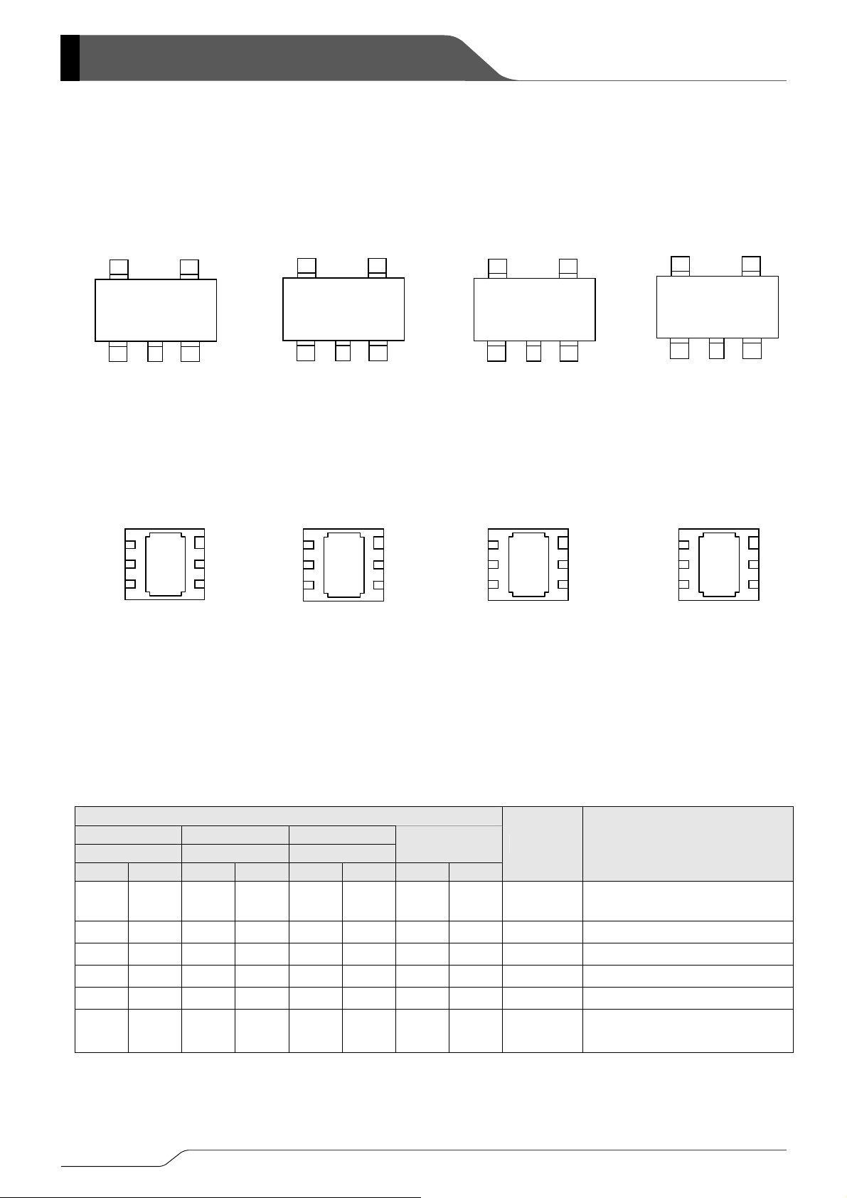
■PIN CONFIGURATION
●SOT-25
XC6101, XC6102 Series
XC6111, XC6112 Series
IN
V
5
WD
4
123
RESETB
MRB
SS
V
SOT-25 (TOP VIEW)
●USP-6C
XC6101, XC6102 Series
XC6111, XC6112 Series
V
V
RESETB
IN
SS
6
5
4
1
2
3
WD
MRB
NC
USP-6C (BOTTOM VIEW)
* The dissipation pad for the USP-6C package should be
solder-plated in reference mount pattern and metal masking
so as to enhance mounting strength and heat release. If
the pad needs to be connected to other pins, it should be
connected to the V
SS (No.5) pin.
■PIN ASSIGNMENT
XC6101, XC6102 XC6103 XC6104, XC6105
XC6111, XC6112 XC6113 XC6114, XC6115
SOT-25 USP-6C SOT-25 USP-6C SOT-25 USP-6C SOT-25 USP-6C
1 4 - - 1 4 1 4
2 5 2 5 2 5 2 5
3 2 3 2 - - 4 1 MRB Manual Reset
4 1 4 1 4 1 - - WD Watchdog
5 6 5 6 5 6 5 6 VIN Power Input
- - 1 4 3 2 3 2 RESET
2/27
XC6103 & XC6113 Series
XC6104, XC6105 Series
XC6114, XC6115 Series
IN
V
5
123
RESET
SOT-25 (TOP VIEW)
XC6103 & XC6113 Series
WD
4
MRB
SS
V
IN
V
5
123
RESETB
SS
V
RESET
SOT-25 (TOP VIEW)
XC6104, XC6105 Series
XC6114, XC6115 Series
V
IN
V
SS
RESET
6
5
4
1
2
3
WD
MRB
NC
V
V
RESETB
IN
6
SS
5
USP-6C (BOTTOM VIEW) USP-6C (BOTTOM VIEW)
PIN NUMBER
XC6116, XC6117
PIN NAME FUNCTION
RESETB
V
SS Ground
XC6116, XC6117 Series
IN
WD
4
V
5
123
RESETB
SOT-25 (TOP VIEW)
XC6116, XC6117 Series
WD
1
RESET
2
34
NC
V
IN
V
SS
RESETB
6
5
4
USP-6C (BOTTOM VIEW)
Reset Output
DFL: Low Level When Detected)
(V
Reset Output
DFH: High Level When Detected)
(V
V
SS
RESET
MRB
4
MRB
1
2
RESET
NC
3
XC6101 ~ XC6105, XC6111~ XC6117
■PRODUCT CLASSIFICATION
●Selection Guide
SERIES WATCHDOG
MANUAL
RESET
VDFL (RESETB) VDFH (RESET)
XC6101 XC6111 Available Available CMOS -
XC6102 XC6112 Available Available N-channel open drain -
XC6103 XC6113 Available Available - CMOS
XC6104 XC6114 Available Not Available CMOS CMOS
XC6105 XC6115 Available Not Available N-channel open drain CMOS
XC6116 Not Available Available CMOS CMOS
XC6117 Not Available Available N-channel open drain CMOS
●Ordering Information
XC61①②③④⑤⑥⑦⑧-⑨
(*1)
DESIGNATOR ITEM SYMBOL DESCRIPTION
① Hysteresis Width
②
Functions and
Type of Reset Output
0 VDF x 5% (TYP.) with hysteresis
1 V
x 0.1% (TYP.) without hysteresis
DF
Watchdog and manual functions, and reset
1 ~ 7
output type as per Selection Guide in the above
chart
A 3.13ms (TYP.)
B 25ms (TYP.)
C 50ms (TYP.)
③ Release Delay Time *
D 100ms (TYP.)
E 200ms (TYP.)
F 400ms (TYP.)
H 1.6s (TYP.)
0
No WD timeout period for
XC6116, XC6117 Series
1 6.25ms (TYP.)
④ Watchdog Timeout Period
2 50ms (TYP.)
3 100ms (TYP.)
4 200ms (TYP.)
5 400ms (TYP.)
6 1.6s (TYP.)
⑤⑥ Detect Voltage 16 ~ 50
MR
⑦⑧-⑨ Packages (Order Unit)
MR-G
ER
ER-G
* Please set the release delay time shorter than or equal to the watchdog timeout period.
ex.) XC6101D427MR or XC6101D327MR
(*1)
The “-G” suffix denotes Halogen and Antimony free as well as being fully RoHS compliant.
Detect voltage
ex.) 4.5V: ⑤⇒4, ⑥⇒5
SOT-25 (3,000/Reel)
SOT-25 (3,000/Reel)
USP-6C (3,000/Reel)
USP-6C (3,000/Reel)
RESET OUTPUT
Series
3/27
,
,
XC6101~XC6105, XC6111~XC6117 Series
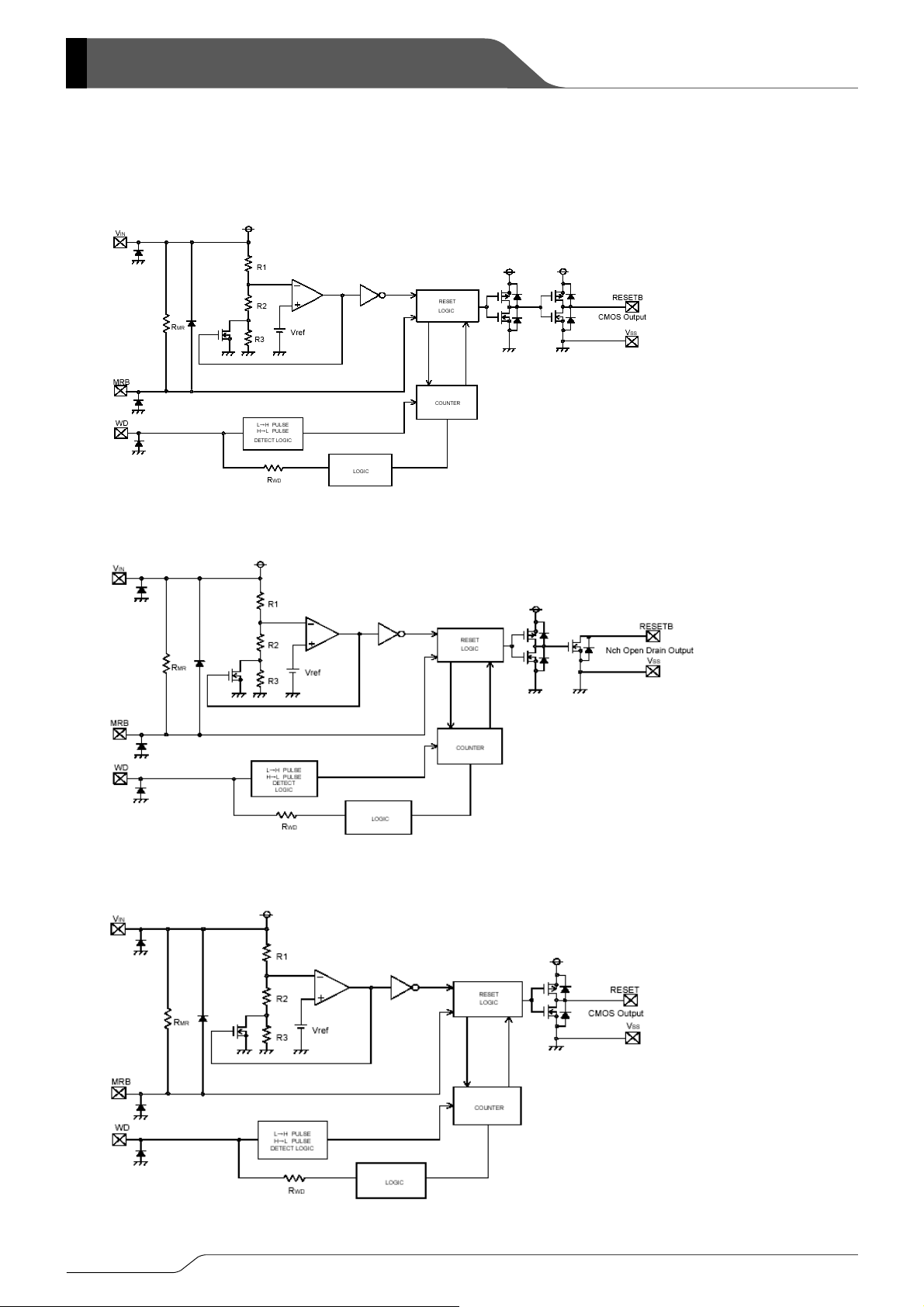
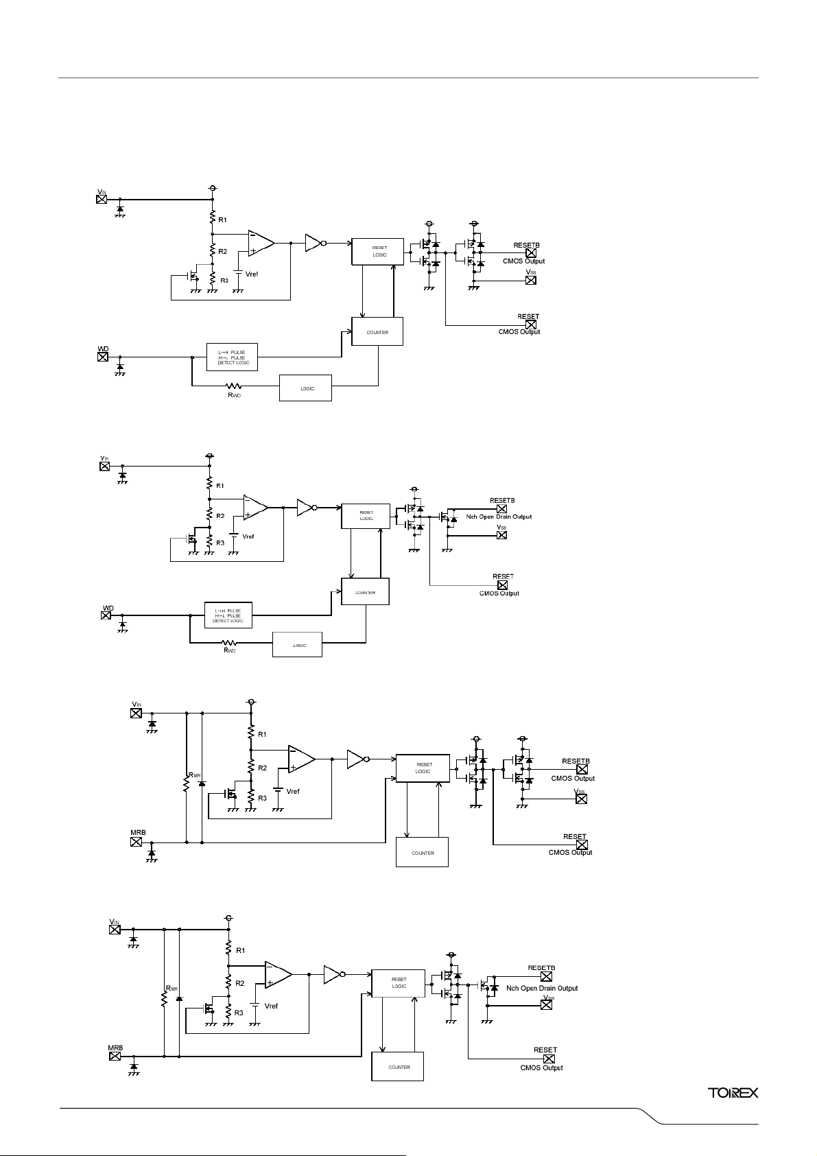
■BLOCK DIAGRAMS
●XC6101, XC6111 S er ies
●XC6102
●XC6103
4/27
XC6112 Series
XC6113 Series
,
,
■BLOCK DIAGRAMS (Continued)
●XC6104
●XC6105
●XC6116 Series
●XC6117 Series
XC6114 Series
XC6115 Series
XC6101 ~ XC6105, XC6111~ XC6117
Series
5/27

XC6101~XC6105, XC6111~XC6117 Series
■ABSOLUTE MAXIMUM RATINGS
PAR AMETER SYMBOL RATINGS UNITS
Input Voltage
Ta = 2 5OC
VIN VSS -0.3 ~ 7.0 V
V
V
MRB
VSS -0.3 ~ 7.0 V
V
WD
-0.3~VIN+0.3≦7.0
SS
V
Output Voltage
Power Dissipation
Output Current I
CMOS Output V
N-ch Open Drain Output V
RBOUT/IROUT
RESETB/VRESET
RESETB
20 mA
V
-0.3~VIN+0.3≦7.0
SS
VSS -0.3 ~ 7.0
SOT-25 250
Pd
USP-6C
100
Operating Ambient Temperature Topr -40 ~ +85
Storage Temperature Tstg -40 ~ +125
V
mW
O
C
O
C
6/27
XC6101 ~ XC6105, XC6111~ XC6117
■ELECTRICAL CHARACTERISTICS
●XC6101~XC6105, XC6111~XC6117 Series
PAR AMETER SYMBOL CONDITIONS MIN. TYP. MAX. UNITS
Detect Voltage
Hysteresis Width
XC6101~XC6105
Hysteresis Width
XC6111~XC6117
(*3)
(*4)
Supply Current ISS
VDFL
VDFH
VHYS
VHYS 0
XC6101~XC6105
XC6111~XC6115
(The MRB & the WD Pin:
No connection)
XC6116/XC6117
(The MRB Pin:
No connection)
VIN=VDF(T)×0.9V - 5 11
VIN=VDF(T)×1.1V - 10 16
IN=6.0V - 12 18
V
VIN=VDF(T)×0.9V - 4 10
VIN=VDF(T)×1.1V - 8 14
IN=6.0V - 10 16
V
VDF(T)
× 0.98
VDF
× 0.02
(*1)
(*2)
VDF(T)
VDF
× 0.05
VDF
× 0.001
VDF(T)
× 1.02
VDF
× 0.08
VDF
x 0.01
Operating Voltage VIN 1.0 - 6.0 V ①
VIN=1.0V 0.15 0.5 -
VIN=2.0V (VDFL(T)> 2.0V) 2.0 2.5 -
VIN=3.0V (VDFL(T) >3.0V) 3.0 3.5 -
V
IN=4.0V (VDFL(T) >4.0V) 3.5 4.0 -
VDFL
Output Current
(RESETB)
N-ch.
VDS = 0.5V
IRBOUT
CMOS,
VIN=6.0V - - 1.1 -0.8
VIN=6.0V 4.4 4.9 - ③
VIN=1.0V - - 0.08 - 0.02
IN=4.0V (VDFH(T)>4.0V) - - 0.95 - 0.75
O
C - +100 - ppm/ OC ①
VDFH
Output Current
(RESET)
Temperature
Coefficient
IROUT
△VDF /
(△To pr・V
DFL
)
P-ch
DS = 0.5V
V
N-ch
VDS = 0.5V
P-ch.
DS = 0.5V
V
-40OC < Topr < 85
VIN=2.0V (VDFH(T)> 2.0V) - - 0.50 - 0.30
VIN=3.0V (VDFH(T)>3.0V) - - 0.75 - 0.55
V
2 3.13 5
18 25 31
Release Delay Time
(VDF<1.8V)
tDR
Time until VIN is increased from
1.0V to 2.0V
and attains to the release time level,
and the Reset output pin inverts.
37 50 63
75 100 125
150 200 250
300 400 500
1200 1600 2000
2 3.13 5
18 25 31
Release Delay Time
(VDF>1.9V)
tDR
Time until VIN is increased from
1.0V to (VDFx1.1V)
and attains to the release time level,
and the Reset output pin inverts.
37 50 63
75 100 125
150 200 250
300 400 500
1200 1600 2000
Time until VIN is decreased from 6.0V to
Detect Delay Time tDF
1.0V and attains to the detect voltage
level, and the Reset output pin detects
- 3 30 μs ⑤
while the WD pin left opened.
V
DFL
Leakage
Current
CMOS
Output
V
CMOS
Output
V
DFL
N-ch Open
Drain
DFH
Nch
I
LEAK
V
V
V
IN=VDFL
=6V, V
IN
=6V, V
IN
×0.9V, V
=0V
RESET
RESETB
RESETB
=6V
=0V
-0.01
0.01 0.1
Output
Ta = 2 5OC
V ①
V ①
V ①
μA ②
mA
mA
ms ⑤
ms ⑤
μA
Series
CIRCUIT
③
④
④
③
7/27
XC6101~XC6105, XC6111~XC6117 Series
■ELECTRICAL CHARACTERISTICS (Continued)
●XC6101~XC6105, XC6111~XC6117 Series
PAR AMETER SYMBOL CONDITIONS MIN. TYP. MAX. UNITS CIRCUIT
Watchdog
Timeout Period
(V
DF<1.8V)
tWD
Watchdog
Timeout Period
(V
DF>1.9V)
Watchdog
Minimum Pulse Width
Watchdog
High Level Voltage
Watchdog
Low Level Voltage
Watchdog
Input Current
Watchdog
Input Resistance
●XC6101 ~ XC6103, XC6111 ~ XC6113, XC6116 , XC6117 Series
tWD
t
WDIN
VIN=VDF x 1.1V ~ 6.0V VIN x 0.7 - 6 V ⑦
V
WDH
V
VIN=VDF x 1.1V ~ 6.0V 0 - VIN x 0.3 V ⑦
WDL
I
WD
RWD VIN=6.0V, VWD=0V, RWD=VIN/ |IWD| 315 500 880 k ⑧
Time until V
the Reset output pin is released to go into
the detection state. (V
Time until V
and the Reset output pin is released to go
into the detection state. (VWD=VSS)
Apply pulse from 6.0V to 0V
VIN=6.0V, VWD=6.0V (Avg. when peak ) - 12 19
VIN=6.0V, VWD=0V (Avg. when peak)
PAR AMETER SYMBOL CONDITIONS MIN. TYP. MAX. UNITS CIRCUIT
MRB
High Level Voltage
MRB
Low Level Voltage
MRB
Pull-up Resistance
MRB Minimum
Pulse Width
(*5)
XC6101~XC6105
V
MRH VIN=VDFx1.1V ~ 6.0V 1.4 - VIN ⑨
V
MRL VIN=VDFx1.1V ~ 6.0V 0 - 0.35
MR VIN=6.0V, MRB=0V, RMR=VIN/ |IMRB| 1.6 2.4 3.0 M ⑩
R
t
MRIN
Apply pulse from 6.0V to 0V to
XC6111~XC6115
MRB Minimum
Pulse Width
(*6)
t
MRIN
Apply pulse from 6.0V to 0V to
XC6116, XC6117
NOTE:
*1: V
*2: If only “V
DF(T): Setting detect voltage
DF” is indicated, it represents both VDFL (low when detected) and VDFH (high when detected).
*3: XC6101~XC6105 (with hysteresis)
*4: XC6111~XC6117 (without hysteresis)
*5: Watchdog function is available.
*6: Watchdog function is not available.
IN increases form
1.0V to 2.0V and
IN increases form
1.0V to (V
DFx1.1V)
IN=6.0V,
V
to the WD pin.
IN=6.0V,
V
the MRB pin
V
IN=6.0V,
the MRB pin
WD=VSS
)
Ta = 2 5OC
4.25 6.25 8.25
37 50 63
75 100 125
150 200 250
ms ⑥
300 400 500
1200 1600 2000
4.25 6.25 8.25
37 50 63
75 100 125
150 200 250
ms ⑥
300 400 500
1200 1600 2000
300 - - ns ⑦
μ
- 19 -12 -
A ⑧
Ta = 2 5
V
2.8 - -
μs ⑪
1.2 - -
⑨
O
C
8/27

XC6101 ~ XC6105, XC6111~ XC6117
Series
■OPERATIONAL EXPLANATION
The XC6101~XC6105, XC6111~XC6117 series compare, using the amplifier, the voltage of the internal voltage reference
source with the voltage divided by R1, R2 and R3 connected to the V
amplifier activates the watchdog logic, manual reset logic, delay circuit and the output driver. When the VIN pin voltage
gradually falls and finally reaches the detect voltage, the RESETB pin output goes from high to low in the case of the VDFL type
ICs, and the RESET pin output goes from low to high in the case of the V
<RESETB / RESET Pin Output Signal>
DFL (RESETB) type - output signal: Low when detected.
* V
The RESETB pin output goes from high to low whenever the VIN pin voltage falls below the detect voltage, or whenever the
MRB pin is driven from high to low. The RESETB pin remains low for the release delay time (tDR) after the VIN pin voltage
reaches the release voltage. If neither rising nor falling signals are applied to the WD pin within the watchdog timeout period,
the RESETB pin output remains low for the release delay time (t
DFH (RESET) type – output signal: High when detected.
* V
The RESET pin output goes from low to high whenever the VIN pin voltage falls below the detect voltage, or whenever the
MRB pin is driven from high to low. The RESET pin remains high for the release delay time (tDR) after the VIN pin voltage
reaches the release voltage. If neither rising nor falling signals are applied to the WD pin within the watchdog timeout period,
OUT pin output remains high for the release delay time (tDR), and thereafter the RESET pin outputs low level signal.
the V
<Hysteresis>
When the internal comparator output is high, the N-Channel transistor connected in parallel to R3 is turned ON, activating the
hysteresis circuit. The difference between the release and detect voltages represents the hysteresis width, as shown by the
following calculations:
DF (detect voltage) = (R1+R2+R3) x Vref(R2+R3)
V
VDR (release voltage) = (R1+R2) x Vref(R2)
HYS (hysteresis width)=VDR-VDF (V)
V
VDR > VDF
* Detect voltage (VDF) includes conditions of both VDFL (low when detected) and VDFH (high when detected).
* Please refer to the block diagr ams for R1, R2, R3 and Vref.
Hysteresis width is selectable from V
<Watchdog (WD) Pin>
The XC6101~XC6105, XC6111~XC6117 series use a watchdog timer to detect malfunction or “runaway” of the
microprocessor. If neither rising nor falling signals are applied from the microprocessor within the watchdog timeout period,
the RESETB/RESET pin output maintains the detection state for the release delay time (t
RESET/RESETB pin output returns to the release state (Please refer to the FUNCTION CHART). The timer in the watchdog
is then restarted. Six watchdog timeout period settings are available in 1.6s, 400ms, 200ms, 100ms, 50ms, 6.25ms.
<MRB Pin>
Using the MRB voltage pin input, the RESET/RESETB pin signal can be forced to the detection state. When the MRB pin is
driven from high to low, the RESETB pin output goes from high to low level signal in the case of the V
RESET pin output goes from low to high in the case of the V
RESET/RESETB pin output maintains the detection state for the release delay time (t
pulled up to the V
which is an input protection element, is connected between the MRB pin and VIN pin. Therefore, if the MRB pin is applied
voltage that exceeds VIN, the current will flow to VIN through the diode. Please use this IC within the stated maximum ratings
-0.3~VIN+0.3≦7.0V) on the MRB pin.
(V
SS
<Release Delay Time>
Release delay time (t
timeout period expires with no rising signal applied to the WD pin, until the RESET/RESETB pin output is released from the
detection state. Seven release delay time (t
100ms, 50ms, 25ms, 3.13ms.
<Detect Delay Time>
Detect Delay Time (t
RESETB pin output goes into the detection state.
IN pin voltage level, leave the MRB pin open if unused (Please refer to the FUNCTION CHART). A diode,
DR) is the time that elapses from when the VIN pin reaches the release voltage, or when the watchdog
DF) is the time that elapses from when the VIN pin voltage falls to the detect voltage until the RESET/
DF x 0.05V (XC6101~XC6105) or VDF x 0.001V (XC6111~XC6117).
) watchdog timeout period settings are available in 1.6s, 400ms, 200ms,
WD
DR), and thereafter the RESET pin outputs high level signal.
DFH type. Even after the MRB pin is driven back high, the
IN pin. The resulting output signal from the error
DFH type ICs.
DR), and thereafter the
DFL type ICs, and the
DR). Since the MRB pin is internally
9/27

XC6101~XC6105, XC6111~XC6117 Series
■TIMING CHARTS
●CMOS Output
10/27
*CMOS output
VDR Level
Level
V
DF
Min.Operating Voltage
GND
WD
GND
MRB
GND
VDR Level
V
Level
DFL
Min.Operating Voltage
Min.Operating Voltage
GND
VDR Level
V
Level
DFH
GND
V
IN
t
WD
Unstable
t
D
R
t
D
R
tWD>t
WDIN
V
Pin Wave Form
IN
Hysterisis Range
t
WD
t
D
R
t
WD
t
MRB>tMRIN
t
D
t
D
R
R
WD Pin Wave Form
MRB Pin Wave Form
RESETB Pin Wave Form(V
RESET Pin Wave Form(V
DFH
)
DFL
)

XC6101 ~ XC6105, XC6111~ XC6117
Series
■NOTES ON USE
1. Please use this IC within the stated maximum ratings. For temporary, transitional voltage drop or voltage rising
phenomenon, the IC is liable to malfunction should the ratings be exceeded.
2. When a resistor is connected between the V
malfunction may occur as a result of the IC’s through current. For the CMOS output products, the V
the IC is operating and malfunction may occur as a result of the IC’s output current. Please be careful with using the
XC6111~XC6117 series (without hysteresis).
3. In order to stabilize the IC’s operations, please ensure that the V
some
4. Noise at the power supply may cause a malfunction of the watchdog operation or the circuit. In such case, please
5. Protecting against a malfunction while the watchdog time out period, an ignoring time (no reaction time) occurs to the rise
6. The watchdog function can be disabled by connecting a three-state device to the WDI pin as a result of the high impedance
The other series is available in the name of XC6121~XC6124 with the ON/OFF control pin for the watchdog function.
7. Torex places an importance on improving our products and its reliability.
● No Reaction Time
μs/V.
strength the line between V
IN and the GND pin and connect about 0.22μF of a capacitor between the VIN pin and the GND
pin.
and fall times. Referring to the figure below, the ignoring time (no reaction time) lasts for 900
state of the WDI pin. This is effective when the watchdog function is not required, for example, during data loading to the
CPU. The WDI input is internally driven through a buffer (LOGIC) and series resistor (R
showed in the block diagrams of page 4 and 5. The WDI input is designed for minimizing the input current by placing the
series resistor (R
) in the maximum resistance of 880kΩ. A voltage drop occurs in proportion to the leakage current of the
WD
three-state device multiplied by the resistance value of the series resistor (R
of high impedance. The voltage level must be reaching the threshold level of the WD so that a three-state device with small
leakage current should be selected.
When these series is used, external parts such as the three-state device is not required.
However, by any possibility, we would request user fail-safe design and post-aging treatment on system or equipment.
IN pin and the input, the VIN voltage drops while the IC is operating and a
IN voltage drops while
IN pin’s input frequency’s rise and fall times are more than
μs at maximum.
) from the watchdog counter as
WD
) when the three-state device is in the state
WD
11/27

XC6101~XC6105, XC6111~XC6117 Series
■PIN LOGIC CONDITIONS
PIN NAME LOGIC CONDITIONS
VIN
MRB
WD
■FUNCTION CHART
●XC6101/XC61111, XC6102/6112 Series
VIN V
H H
H L
H Open
H
H
H
L
●XC6103/XC61113 Series
VIN V
H H
H L
H Open
H
H
H
L
●XC6104/XC61114, XC6105/XC6115 Series
●XC6104/XC61114, XC6105/XC6115 Series
VIN VWD V
H H
H L
H Open
H
H
L
●XC61116, XC6117 Series
*1: Including all logic of WD (VWD=H, L, L→H, H→L, OPEN).
*2: When the V
When the V
*3: When the V
When the V
*4: V
IN=L and V
*5: The RESET/RESETB pin becomes indefinite operation while 0.35V<V
H VIN>VDF+VHYS
L V
H V
L V
H When keeping VWD>V
L When keeping VWD <V
L → H V
H → L V
VWD V
MRB
WDL
WDH
→ V
→V
IN<VDF
>1.40V
MRB
<0.35V
MRB
WDH
WDH
more than tWD
WDH
more than tWD
WDL
, t
>300ns
WDIN
, t
>300ns
WDIN
Repeat detect and release (H→L→H)
H or Open
L → H
H → L
L *1 L
VWD V
MRB
Repeat detect and release (L→H→L)
H or Open
L → H
H → L
L *1 H
(*2)
RESETB
V
Repeat detect and release (H→L→H) Repeat detect and release (L→H→L)
L → H
H L
H → L
*1 L H
VIN V
V
MRB
H H or Open H L
H
L
is High, the circuit is in the release state.
RESETB
is Low, the circuit is in the detection state.
RESETB
is Low, the circuit is in the release state.
RESET
is High, the circuit is in the detection state.
RESET
=H can not be combined for the rated input voltage of the V
MRB
L L H
MRB
NOTE:
*1: If only “V
detected) and V
*2: For the details of each parameter, please see the electrical
characteristics.
RESETB
H
(*3)
RESET
L
(*2)
RESETB
pin is Vss-0.3V to VIN+0.3V.
MRB
<1.4V.
V
DF” is indicated, it represents both VDFL (low when
DFH (high when detected).
V
DF: Detect Voltage
V
: Hysteresis Width
HYS
: WD High Level Voltage
V
WDH
V
: WD Low Level Voltage
WDL
: WD Pulse Width
t
WDIN
: WD Timeout Period
t
WD
(*2)
(*3)
RESET
RESET
(*3)
12/27

■TEST CIRCUITS
Circuit 1 Circuit 2
Circuit 3
Circuit 4
VDS=0.5V
When measuring leak
V
RESETB
V
RESETB
XC6101 ~ XC6105, XC6111~ XC6117
Series
=0V (CMOS Output (Pch))
=6V (Nch Open Drain Output)
13/27

XC6101~XC6105, XC6111~XC6117 Series
■TEST CIRCUITS (Continued)
Circuit 5
Circuit 6
Circuit 7
14/27
100kΩ
(Unused for CMOS
output products.)
Measuring
waveform

■TEST CIRCUITS (Continued)
Circuit 8 Circuit 9
Circuit 10
Circuit 11
XC6101 ~ XC6105, XC6111~ XC6117
Series
100kΩ
(Not used when the CMOS
Output products selected.)
100kΩ
(Unused for CMOS
output products.)
Measuring
waveform
15/27

XC6101~XC6105, XC6111~XC6117 Series
■TYPICAL PERFORMANCE CHARACTERISTICS
(1.1) Supply Current vs. Input Voltage
XC61X1~XC61X5 (1.6V)
30
25
20
ISS (μA)
Ta= 25
15
10
Supply Current: ISS (μA)
Supply Current:
5
0
0123456
30
25
20
ISS (μA)
15
10
Supply Current:
Supply Current: ISS (μA)
5
0
0123456
℃
Input Voltage: VIN (V)
Input Voltage: VIN (V)
XC61 X1 ~ XC61 X5 (5 . 0V)
Ta= 25
℃
Input Voltage: VIN (V)
Input Voltage: VIN (V)
(1.2) Supply Current vs. Input Voltage
XC6116, XC6117(1.6V) XC6116, XC6117(2.7V)
30
25
20
ISS (μA)
15
10
Supply Current:
Supply Current: ISS (μA)
5
0
0123456
XC61X6~XC61X7 (1.6V)
Ta= 25
Input Voltage: VIN (V)
Input Voltage: VIN (V)
* ‘X’ represents both ‘0’ and ‘1’. (ex. XC61X1⇒XC6101 and XC6111)
Ta= 85
℃
Ta= -40
℃
Ta= 85
Ta= -40
℃
℃
Ta= 85
Ta= -40
℃
℃
30
25
20
ISS (μA)
15
10
Supply Current: ISS (μA)
Supply Current:
5
0
0123456
℃
30
25
20
ISS (μA)
15
10
Supply Current: ISS (μA)
Supply Current:
5
0
0123456
XC61X1~XC61X5 (2.7V)
Input Voltage: VIN (V)
Input Voltage: VIN (V)
XC61X6~XC61X7 (2.7V)
Input Voltage: VIN (V)
Input Voltage: VIN (V)
Ta= 25
Ta= 25
℃
℃
Ta= 85
Ta= -40
Ta= 85
Ta= -40
℃
℃
℃
℃
16/27

A
A
A
XC6101 ~ XC6105, XC6111~ XC6117
■TYPICAL PERFORMANCE CHARACTERISTICS (Continued)
(1.2) Supply Current vs. Input Voltage (Continued)
Series
ISS (μA)
Supply Current:
Supply Current: ISS (μA)
30
25
20
15
10
XC6116, XC6117(5.0V)
XC61X6~XC61X7 (5.0V)
5
0
0123456
Ta= 25
℃
Input Voltage: VIN (V)
Input Voltage: VIN (V)
Ta= 85
Ta= -40
℃
℃
(2) Detect, Release Voltage vs. Ambient Temperature
1.70
1.65
1.60
Detect, Release V oltage: VDF,VDR (V)
Detect, Release Voltage: VDF, VDR (V)
1.55
-50 -25 0 25 50 75 100
5.30
5.20
5.10
5.00
Detect, Release V oltage: VDF,VDR (V)
Detect, Release Voltage: VDF, VDR (V)
4.90
-50 -25 0 25 50 75 100
XC61X1~XC61X7 (1.6V)
VDR
VDF
Ambient Temperature: Ta (℃)
mbient Temperature: Ta (℃)
XC61X1~XC61X7 (5.0V)
VDR
VDF
Ambient Temperature: Ta (℃)
mbient Temperature: Ta (℃)
* ‘X’ represents both ‘0’ and ‘1’. (ex. XC61X1⇒XC6101 and XC6111)
XC61X1~XC61X7 (2.7V)
2.90
2.80
2.70
Detect, Release V oltage: VDF,VDR (V)
2.60
-50-25 0 255075100
Ambient Temperature: Ta (℃)
mbient Temperature: Ta (℃)
VDR
VDF
17/27

XC6101~XC6105, XC6111~XC6117 Series
■TYPICAL PERFORMANCE CHARACTERISTICS (Continued)
(3-1) Output Voltage vs. Input Voltage (VDFL)
(3.1) Detect, Release Voltage vs. Input Voltage (VDFL)
XC6101~XC6105(1.6V) XC6101~XC6105(2.7V)
2.0
1.5
1.0
0.5
Detect, Release Voltage:VDFL,VDR(V)
0.0
Detect, Release Voltage: VDFL, VDR (V)
012
6.0
5.0
4.0
3.0
2.0
1.0
Detect, Release Voltage: VDFL, VDR (V)
Detect, Release Voltage:VDFL,VDR(V)
0.0
XC6101~ XC6107 (1.6V )
Rpull:100kΩ
Ta= -40
℃
25
℃
85
℃
VDF
↓:
VDR
↑:
Input Voltage: VIN (V)
Input Voltage: VIN (V)
XC6101~XC6105(5.0V)
XC6101~ XC6107 (5.0V)
Rpull:100kΩ
Ta= -40
℃
25
℃
85
℃
VDF
↓:
VDR
↑:
0123456
Input Voltage: VIN (V)
Input Voltage: VIN (V)
(3.2) Detect, Release Voltage vs. Input Voltage (VDFH)
Detect,Release Voltage:VDR,VDFH(V)
Detect, Release Voltage: VDR, VDFH (V)
* ‘X’ represents both ‘0’ and ‘1’. (ex. XC61X1⇒XC6101 and XC6111)
XC6103~XC6105(1.6V) XC6103~XC6105(2.7V)
XC6103~ XC6107 (1.6V )
Rpull:100kΩ
Ta= -40
℃
25
℃
85
℃
VDF
↑:
VDR
↓:
012
Input Voltage: VIN (V)
Input Voltage: VIN (V)
2.0
1.5
1.0
0.5
0.0
XC6101~ XC6107 (2.7V )
3.0
2.5
2.0
1.5
1.0
0.5
Detect, Release Voltage:VDFL,VDR(V)
0.0
Detect, Release Voltage: VDFL, VDR (V)
Rpull:100kΩ
Ta= -40
℃
25
℃
85
℃
VDF
↓:
VDR
↑:
0123
Input Voltage: VIN (V)
Input Voltage: VIN (V)
XC6103~ XC6107 (2.7V )
3.0
Rpull:100kΩ
Ta= -40
2.5
2.0
1.5
1.0
0.5
Detect,Release Voltage:VDR,VDFH(V)
Detect, Release Voltage: VDR, VDFH (V)
0.0
0123
℃
25
℃
85
℃
VDF
↑:
VDR
↓:
Input Voltage: VIN (V)
Input Voltage: VIN (V)
18/27

XC6101 ~ XC6105, XC6111~ XC6117
■TYPICAL PERFORMANCE CHARACTERISTICS (Continued)
(3.2) Detect, Release Voltage vs. Input Voltage (VDFH) (Continued)
XC6103~ XC6107 (5.0V)
6.0
5.0
4.0
3.0
2.0
1.0
Detect,Release Voltage:VDR,VDFH(V)
0.0
Detect, Release Voltage: VDR, VDFH (V)
(4) N-ch Driver Output Current vs. VDS
Output Current: IOUT (mA)
XC6103~XC6105(5.0V)
Rpull:100kΩ
Ta= -40
℃
25
℃
85
℃
VDF
↑:
VDR
↓:
0123456
Input Voltage: VIN (V)
Input Voltage: VIN (V)
XC61X1~XC61X7
6
Ta= 25
℃
5
4
3
2
1
0
0123
VIN=1.0V
VDS (V)
VIN=2.0V
(5) N-ch Driver Output Current vs. Input Voltage
6.0
VDS=0.5V
5.0
4.0
3.0
2.0
1.0
Output Current: IOUT (mA)
0.0
0123456
* ‘X’ represents both ‘0’ and ‘1’. (ex. XC61X1⇒XC6101 and XC6111)
XC61X1~XC61X7
Ta= -40
℃
Ta= 25
Input Voltage: VIN (V)
Ta= 85
℃
℃
20
Ta= 25
16
12
8
4
Output Current: IOUT (mA)
0
0123456
XC61X1~XC61X7
℃
VIN=3.0V
VDS (V)
Series
VIN=4.0V
19/27

XC6101~XC6105, XC6111~XC6117 Series
■TYPICAL PERFORMANCE CHARACTERISTICS (Continued)
(6) P-ch Driver Output Current vs. Input Voltage 1
6.0
5.0
4.0
3.0
2.0
Output Current: IOUT (mA)
1.0
0.0
(8) Release Delay Time vs. Ambient Temperature
6.0
)
5.0
msec
(
4.0
TDR
(ms)
DR
3.0
2.0
1.0
Release Delay Time
Release Delay Time t
0.0
3000
)
2500
msec
(
2000
(ms)
TDR
DR
1500
1000
500
Release Delay Time
Release Delay Time t
* ‘X’ represents both ‘0’ and ‘1’. (ex. XC61X1⇒XC6101 and XC6111)
XC61X1, XC61X3~ XC61X7
Ta= 25
℃
VDS=2.0V
1.5V
1.0V
0.5V
0123456
0
Input Voltage: VIN (V)
XC61X1~XC61X7
TDR=3.13msec
tDR=3.13ms tDR =100ms
-50-25 0 255075100
Ambient Temperature: Ta (℃)
XC61X1~XC61X7
TDR=1.6sec
tDR =1.6s
-50 -25 0 25 50 75 100
Ambient Temperature: Ta (℃)
(7) P-ch Driver Output Current vs. Input Voltage 2
XC61X1, XC61X3~ XC61X7
2.0
VDS=0.5V
1.6
Ta= -40
Ta= 85
℃
℃
1.2
Ta= 25
0.8
0.4
Output Current: IOUT (mA)
0.0
01234 56
300
)
msec
(
TDR
Release Delay Time
Release Delay Time tDR (ms)
TDR=100msec
250
200
150
100
50
0
-50 -25 0 25 50 75 100
℃
Input Voltage: VIN (V)
XC61X1~XC61X7
Ambient Temperature: Ta (℃)
20/27

XC6101 ~ XC6105, XC6111~ XC6117
■TYPICAL PERFORMANCE CHARACTERISTICS (Continued)
(9) Watchdog Timeout Period vs. Ambient Temperature
12
)
msec
(
(ms)
WD
TWD=6.25msec
TWD=6.25m
tWD=6.25ms
10
8
6
4
2
WD Timeout Piriod TWD
WD Timeout Period t
0
-50-25 0 255075100
3000
)
2500
msec
(
(ms)
2000
WD
1500
1000
500
WD Timeout Period t
WD Timeout Piriod TWD
0
-50 -25 0 25 50 75 100
XC61X1~XC61X5
Ambient Temperature: Ta (℃)
XC61X1~XC61X5
TWD=1.6sec
tWD =1.6s
Ambient Temperature: Ta (℃)
(10) Release Delay Time vs. Input Voltage
120
)
msec
(
(ms)
DR
110
100
90
Ta= 25
TDR=100msec
80
70
Release Delay Time : TDR
Release Delay Time t
60
12345 67
* ‘X’ represents both ‘0’ and ‘1’. (ex. XC61X1⇒XC6101 and XC6111)
XC61x 1~XC61x7
℃
Ta =2 5 ℃
t
=100ms
WD
Input Voltage: VIN (V)
300
)
250
msec
(
200
150
100
50
WD Timeout Piriod TWD
WD Timeout Period tWD (ms)
0
-50 -25 0 25 50 75 100
XC61X1~XC61X5
TWD=100msec
tWD =100ms
Ambient Temperature: Ta (℃)
(11) Watchdog Timeout Period vs. Input Voltage
XC61x 1~XC61x5
120
(ms)
WD
WD Timeout Period t
)
msec
(
WD Timeout Piriod : TWD
Ta= 25
℃
Ta =2 5 ℃
TWD=100msec
t
=100ms
WD
110
100
90
80
70
60
1234567
Input Voltage: VIN (V)
Series
21/27

XC6101~XC6105, XC6111~XC6117 Series
■TYPICAL PERFORMANCE CHARACTERISTICS (Continued)
(12) Watchdog Low Level Voltage vs. Ambient Temperature (13) Watchdog High Level Voltage vs. Ambient Temperature
6.0
5.0
4.0
3.0
VWDL(V)
2.0
1.0
WD LowLevel Threshold Voltage
0.0
-50 -25 0 25 50 75 100
XC61X1~XC61X5
VIN=6.0V
VIN=3.0V
VIN=1.76V
Ambient Temperature: Ta (℃)
XC61X1~XC61X5
6.0
5.0
Voltage
4.0
3.0
VWDH(V)
2.0
1.0
WD HighLevel Threshold
0.0
-50 -25 0 25 50 75 100
Ambient Temperature: Ta (℃)
VIN=6.0V
VIN=3.0V
VIN=1.76V
(14) MRB Low Level Voltage vs. Ambient Temperature (15) MRB High Level Voltage vs. Ambient Temperature
* ‘X’ represents both ‘0’ and ‘1’. (ex. XC61X1⇒XC6101 and XC6111)
XC61X1~XC61X3, XC6116, XC6117 XC61X1~XC61X3, XC6116, XC6117
MRB LowLevel Threshold V oltage
XC61X1~XC61X3, XC61X6~XC61X7
1.10
1.00
0.90
VIN=3.0V
0.80
VMRL(V)
0.70
0.60
VIN=1.76V
0.50
-50 -25 0 25 50 75 100
Ambient Temperature: Ta (℃)
VIN=6.0V
VMRH(V)
MRB HighLevel Threshold V oltage
XC61X1~XC61X3, XC61X6~XC61X7
1.10
1.00
0.90
0.80
0.70
0.60
0.50
-50-25 0 255075100
Ambient Temperature: Ta (℃)
VIN=6.0V
VIN=3.0V
VIN=1.76V
22/27

■PACKAGING INFORMATION
●SOT-25
●USP-6C Reference Pattern Layout
(Reference)
0.225
0.50.5
0.25
0.250.25
1.6
1.8
XC6101 ~ XC6105, XC6111~ XC6117
●USP-6C
1.8±0.05
1pin INDENT
0.05
0.30±0.05
(0.1)
(0.50)
0.10±0.05
1.4±0.05
●USP-6C Reference Metal Mask Design
(Reference)
0.225
0.50.5
0.20±0.05
0.6
Series
0.25
0.250.25
1.4
1.2
23/27

XC6101~XC6105, XC6111~XC6117 Series
■MARKING RULE
●SOT-25
①②③④
② represents release delay time and watchdog timeout period
MARK
③ represents detect voltage
XC6101/11/02/12/03/13/04/14/15/16/17Series
RELEASE
DELAY
TIME
A 3.13ms XC6116, XC6117 series XC61xxA0xxxx E 50ms 400ms XC61xxC5xxxx
0 3.13ms 6.25ms XC61xxA1xxxx F 50ms 1.6s XC61xxC6xxxx
1 3.13ms 50ms XC61xxA2xxxx D 100ms XC6116, XC6117 series XC61xxD0xxxx
2 3.13ms 100ms XC61xxA3xxxx H 100ms 100ms XC61xxD3xxxx
3 3.13ms 200ms XC61xxA4xxxx K 100ms 200ms XC61xxD4xxxx
4 3.13ms 400ms XC61xxA5xxxx L 100ms 400ms XC61xxD5xxxx
5 3.13ms 1.6s XC61xxA6xxxx M 100ms 1.6s XC61xxD6xxxx
B 25ms XC6116, XC6117 series XC61xxB0xxxx E 200ms XC6116, XC6117 series XC61xxE0xxxx
6 25ms 50ms XC61xxB2xxxx P 200ms 200ms XC61xxE4xxxx
7 25ms 100ms XC61xxB3xxxx R 200ms 400ms XC61xxE5xxxx
8 25ms 200ms XC61xxB4xxxx S 200ms 1.6s XC61xxE6xxxx
9 25ms 400ms XC61xxB5xxxx F 400ms XC6116, XC6117 series XC61xxF0xxxx
A 25ms 1.6s XC61xxB6xxxx T 400ms 400ms XC61xxF5xxxx
C 50ms XC6116, XC6117 series XC61xxC0xxxx U 400ms 1.6s XC61xxF6xxxx
B 50ms 50ms XC61xxC2xxxx H 1.6s XC6116, XC6117 series XC61xxH0xxxx
C 50ms 100ms XC61xxC3xxxx V 1.6s 1.6s XC61xxH6xxxx
D 50ms 200ms XC61xxC4xxxx
MARK DETECT VOLTAGE PRODUCT SERIES MARK DETECT VOLTAGE PRODUCT SERIES
F 1.6 XC61Xxxx16xx 3 3.4 XC61Xxxx34xx
H 1.7 XC61Xxxx17xx 4 3.5 XC61Xxxx35xx
K 1.8 XC61Xxxx18xx 5 3.6 XC61Xxxx36xx
L 1.9 XC61Xxxx19xx 6 3.7 XC61Xxxx37xx
M 2.0 XC61Xxxx20xx 7 3.8 XC61Xxxx38xx
N 2.1 XC61Xxxx21xx 8 3.9 XC61Xxxx39xx
P 2.2 XC61Xxxx22xx 9 4.0 XC61Xxxx40xx
R 2.3 XC61Xxxx23xx A 4.1 XC61Xxxx41xx
S 2.4 XC61Xxxx24xx B 4.2 XC61Xxxx42xx
T 2.5 XC61Xxxx25xx C 4.3 XC61Xxxx43xx
U 2.6 XC61Xxxx26xx D 4.4 XC61Xxxx44xx
V 2.7 XC61Xxxx27xx E 4.5 XC61Xxxx45xx
X 2.8 XC61Xxxx28xx F 4.6 XC61Xxxx46xx
Y 2.9 XC61Xxxx29xx H 4.7 XC61Xxxx47xx
Z 3.0 XC61Xxxx30xx K 4.8 XC61Xxxx48xx
0 3.1 XC61Xxxx31xx L 4.9 XC61Xxxx49xx
1 3.2 XC61Xxxx32xx M 5.0 XC61Xxxx50xx
2 3.3 XC61Xxxx33xx
WATCH DOG
TIMEOUT PERIOD
① represents product series
MARK PRODUCT SERIES MARK PRODUCT SERIES
0 XC6101xxxxxx 8 XC6112xxxxxx
1 XC6102xxxxxx 9 XC6113xxxxxx
2 XC6103xxxxxx A XC6114xxxxxx
3 XC6104xxxxxx B XC6115xxxxxx
4 XC6105xxxxxx C XC6116xxxxxx
7 XC6111xxxxxx D XC6117xxxxxx
PRODUCT
SERIES
MARK
RELEASE
DELAY
TIME
WATCH DOG
TIMEOUT PERIOD
PRODUCT
SERIES
24/27

)
XC6101 ~ XC6105, XC6111~ XC6117
■MARKING RULE (Continued
③ represents detect voltage
XC6105 Series
MARK DETECT VOLTAGE PRODUCT SERIES MARK DETECT VOLTAGE PRODUCT SERIES
F 1.6
H 1.7
K 1.8
L 1.9
M 2.0
N 2.1
P 2.2
R 2.3
S 2.4
T 2.5
U 2.6
V 2.7
X 2.8
Y 2.9
Z 3.0
0 3.1
1 3.2
2 3.3
XC6105XX16XX
XC6105XX17XX
XC6105XX18XX
XC6105XX19XX
XC6105XX20XX
XC6105XX21XX
XC6105XX22XX
XC6105XX23XX
XC6105XX24XX
XC6105XX25XX
XC6105XX26XX
XC6105XX27XX
XC6105XX28XX
XC6105XX29XX
XC6105XX30XX
XC6105XX31XX
XC6105XX32XX
XC6105XX33XX
3 3.4
4 3.5
5 3.6
6 3.7
7 3.8
8 3.9
9 4.0
A 4.1
B 4.2
C 4.3
D 4.4
E 4.5
F 4.6
H 4.7
K 4.8
L 4.9
M 5.0
④ represents production lot number
0 to 9 and A to Z and inverted 0 to 9 and A to Z repeated. (G, I, J, O, Q, W excluded.)
XC6105XX34XX
XC6105XX35XX
XC6105XX36XX
XC6105XX37XX
XC6105XX38XX
XC6105XX39XX
XC6105XX40XX
XC6105XX41XX
XC6105XX42XX
XC6105XX43XX
XC6105XX44XX
XC6105XX45XX
XC6105XX46XX
XC6105XX47XX
XC6105XX48XX
XC6105XX49XX
XC6105XX50XX
Series
25/27

XC6101~XC6105, XC6111~XC6117 Series
■MARKING RULE (Continued)
●USP-6C
0 to 9 and A to Z repeated. (G, I, J, O, Q, W excluded.)
X No character inversion used.
① represents product series
MARK PRODUCT SERIES MARK PRODUCT SERIES
3 XC6101xxxxxx 9 XC6112xxxxxx
4 XC6102xxxxxx A XC6113xxxxxx
5 XC6103xxxxxx B XC6114xxxxxx
6 XC6104xxxxxx C XC6115xxxxxx
7 XC6105xxxxxx 8 XC6116xxxxxx
8 XC6111xxxxxx 9 XC6117xxxxxx
② represents release delay time
MARK RELEASE DELAY TIME PRODUCT SERIES
A 3.13ms XC61XxAxxxxx
B 25ms XC61XxBxxxxx
C 50ms XC61XxCxxxxx
D 100ms XC61XxDxxxxx
E 200ms XC61XxExxxxx
F 400ms XC61XxFxxxxx
H 1.6s XC61XxHxxxxx
③ represents watchdog timeout period
MARK WATCHDOG TIMEOUT PERIOD PRODUCT SERIES
0 XC6116, XC6117 series XC61Xxx0xxxx
1 6.25ms XC61Xxx1xxxx
2 50ms XC61Xxx2xxxx
3 100ms XC61Xxx3xxxx
4 200ms XC61Xxx4xxxx
5 400ms XC61Xxx5xxxx
6 1.6s XC61Xxx6xxxx
④⑤ represents detect voltage
MARK
④ ⑤
DETECT VOLTAGE (V) PRODUCT SERIES
3 3 3.3 XC61Xxxx33xx
5 0 5.0 XC61Xxxx50xx
⑥ represents production lot number
XX ‘X’ represents both ‘0’ and ‘1’. (ex. XC61X1⇒XC6101 and XC6111)
26/27

XC6101 ~ XC6105, XC6111~ XC6117
Series
1. The products and product specifications contained herein are subject to change without
notice to improve performance characteristics. Consult us, or our representatives
before use, to confirm that the information in this datasheet is up to date.
2. We assume no responsibility for any infringement of patents, patent rights, or other
rights arising from the use of any information and circuitry in this datasheet.
3. Please ensure suitable shipping controls (including fail-safe designs and aging
protection) are in force for equipment employing products listed in this datasheet.
4. The products in this datasheet are not developed, designed, or approved for use with
such equipment whose failure of malfunction can be reasonably expected to directly
endanger the life of, or cause significant injury to, the user.
(e.g. Atomic energy; aerospace; transport; combustion and associated safety
equipment thereof.)
5. Please use the products listed in this datasheet within the specified ranges.
Should you wish to use the products under conditions exceeding the specifications,
please consult us or our representatives.
6. We assume no responsibility for damage or loss due to abnormal use.
7. All rights reserved. No part of this datasheet may be copied or reproduced without the
prior permission of TOREX SEMICONDUCTOR LTD.
27/27
 Loading...