

A
XC3202B Series
ETR2602-005a
Low Power Consumption Hall IC (Magnetic Sensor)
■GENERAL DESCRIPTIO N
The XC3202B series is a Hall effect magnetic sensor IC with a built-in CMOS output driver. The device features low power
consumption and small packaging which is ideally suited fo r battery powered portable applications s uch as mobile phones,
electronic dictionaries and handheld game consoles. When the magnetic flux density is higher than the operating point
(Bop), the Low level signal is output. The High level signal is output when the mag netic flux density is lower than the
release point (Brp).
■
PPLICATIONS
●Cover detectors
●Mobile phones
●Electronic dictionaries
●
Portable game consoles
●
Home electronics (refrigerators, washing machines etc)
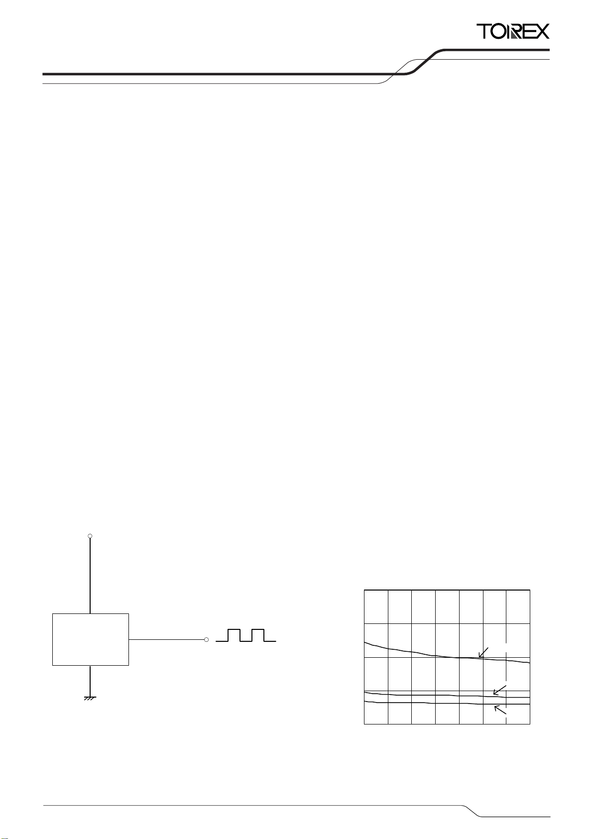
■TYPICAL APPLICATION CIRCUIT
C: Capacitor to stabilize input voltage and decrease noise.
V
DD
XC3202
V
V
OUT
OUTPUT
SS
Recommendation value: 10nF~100nF
■FEATURES
Supply Voltage Range
Average Supply Current : 8μA
Operating Point : South Pole 3mT(TYP.)
North Pole -3mT(TYP.)
Release point : South Pole 2mT(TYP.)
Hysteresis Width : South Pole 1mT(TYP.)
Packages : SOT-23D
QFN-0601
Environmentally Friendly
: 2.4~5.5V
North Pole -2mT(TYP.)
North Pole 1mT(TYP.)
: EU RoHS Compliant, Pb Free
■ TYPICAL PERFORMANCE
CHARACTERISTICS
●Supply Current (avg) vs. Ambient Temperature
40
(μA)
DD
30
VIN=5.5V
20
3.0V
10
Average Supply Current:I
0
-40-200 20406080100
Ambient Temperature:Ta (℃)
2.4V
1/9
XC3202B Series
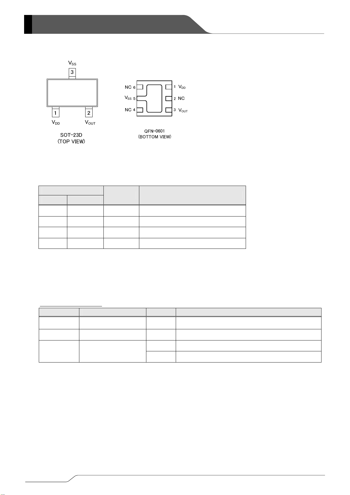
■PIN CONFIGURATION
■PIN ASSIGNMENT
PIN NUMBER
SOT-23D QFN-0601
PIN NAME FUNCTION
1 1 VDD Power Input
2 3 V
Output Pin
OUT
3 5 VSS Ground
- 2,4,6 NC No Connection
■PRODUCT CLASSIFICATION
●Ordering Information
XC3202①②③④⑤⑥-⑦
(*1)
DESIGNATOR ITEM SYMBOL
①
②③④
⑤⑥-⑦
(*1)
The “-G” suffix indicates that the products are Halogen and Antimony free as well as being fully RoHS compliant.
Product Type B CMOS Output
Product No. 183 Based on the internal standard
Packages (Order Unit)
2/9
DESCRIPTION
MR-G SOT-23D (3,000/Reel)
ZR-G QFN-0601 (3,000/Reel)
A
■BLOCK DIAGRAMS
■
Hall Plate
Hall Plate
BSOLUTE MAXIMUM RATINGS
PARAMETER SYMBOL RATINGS UNITS
Amp
Amp
V
DD
Power
switch
Latch
Latch
Logical
XC3202B
Series
V
OUT
V
SS
Ta=25℃
Supply Voltage VDD 7 V
Magnetic Flux Density B Unlimited -
Operating T emperature Range Topr
Storage Temperature Range Tstg
Power Dissipation
SOT-23D 150
QFN-0601
Pd
-40~+85 ℃
-55~+150 ℃
120
Maximum Junction Temperature Tjc 125
Maximum Output Current I
(*1) This IC should be used within the stated absolute maximum ratings in order to prevent damage.
■ELECTRICAL CHARACTERISTICS
40 mA
OUT
PARAMETER SYMBOL CONDITONS MIN. TYP. MAX. UNITS
Output ON Voltage (High)
Output ON Voltage (Low)
V
OUT_H
V
OUT_L
V
=3V, I
DD
V
=3V, I
DD
=-1mA VDD-0.2 - -
OUT
OUT
=1mA
- - 0.1
IDD (en) VDD=3V - 3 6 mA
Supply Current
Detection Time
Detection Period
Duty Cycle
(*1)
(*1)
IDD (dis) VDD=3V - 5 10
I
(avg) VDD=3V - 8 16
DD
t_awake
t_period
DTY
VDD=3V - 75 150
VDD=3V - 75 150
- 0.1 -
Power Supply Voltage VDD 2.4 - 5.5 V
(*1) Normal operation starts 150ms later from the supply voltage (V
(*2) For supply current, detection time, and detection period, please refer to the below.
The Hall IC is operated intermittently to reduce supply current.
Measurement is done during detection time, in the rest period sensing circuits of Hall plate and latch are turned off to minimize the current.
IDD(en)
IDD(dis)
両極探知ホールICは間欠動作によって消費電流を低減しています。
検出動作時間内で磁気の探知を行い検出動作時間以外はHall Plate,Latchなどの探知回路を
OFFにして電流を抑えています。
t_awake
=2.4~5.5V)
DD
t_period
mW
℃
Ta=25℃
CIRCUIT
V
③
②
μA ①
μA ②
μs
ms
%
②
②
3/9

XC3202B Series
■MAGNETIC STATE CHARACTERISTICS
PARAMETER SYMBOL MIN. TYP. MAX. UNITS
Operating Magnetic Flux Density: South Pole Bops 2 3 4 mT
Operating Magnetic Flux Density: North Pole Bopn -4 -3 -2 mT
Release Magnetic Flux Density: South Pole Brps 1 2 - mT
Release Magnetic Flux Density: North Pole Brpn - -2 -1 mT
Hysteresis Width Bhy(Bop-Brp) 0.5 1 - mT
* Characteristics Values are guaranteed in design. The values may be affected by the conditions such as temperature and mounting.
●Magnetic field and detect surface
The IC Hall plates detect the perpendicular magnetic field so that IC surface should be placed in a
direction perpendicular to the magnetic field.
■OPERATIONAL
●Operating by flux density
●Timing chart
I
DD
B
Bop
VOUT
High
Low
*1: When the magnetic flux density to the IC becomes larger than Bop, the IC goes into an on-state and outputs a low signal (V
leading edge of the next “tawake” pulse.
*2: When the magnetic flux density to the IC becomes lower than Brp, the IC goes into an off-state and outputs a high signal (V
leading edge of the next “tawake” pulse.
During the other periods, the previous state is maintained.
Time
V
(off-state)
DD
ON
Bhy
(on-state)
Bopn Brpn
North Pole magnetic flux density
Output Voltage
OFF
0
t_period Time
t_awake Time
*1
Output Voltage
South Pole magnetic flux density
DD
I
B
Brp
VOUT
High
Low
Ta=25℃, VDD=3V, 1mT=10Gauss
(off-state)
OFF
0
Bhy
V
DD
ON
(on-state)
BopsBrps
t_period Time
t_awake Time
Time
CIRCUIT
③
③
③
③
③
*2
=Low) at the
OUT
=High) at the
OUT
4/9

5
■NOTES ON USE
1. The magnetic flux density will be changed when an external capacitor (CIN) is connected between VDD and VSS.
North Pole Magnetic Flux Density vs. Input Capacitance (CIN)
North P ole magnetic flux density
XC3202B
Series
-4.0
-3.5
-3.0
-2.5
-2.0
-1.5
-1.0
magnetic flux density(mT)
-0.5
0.0
0.001 0.01 0.1 1 10
Ceramic Capacitor CIN(μF)
South Pole Magnetic Flux Density vs. Input Capacitance (C
VIN=3V,Ta=2
Operating
Release
℃
)
IN
South P ole magnetic flux density
4.0
3.5
3.0
2.5
2.0
1.5
1.0
magnetic flux density(mT)
0.5
0.0
0.001 0.01 0.1 1 10
Ceramic Capacitor CIN (μF)
VIN=3V,Ta=25
Operating
Release
℃
2. Please use this IC within the stated maximum ratings. For temporary, transitional voltage drop or voltage rising phenomenon,
the IC is liable to malfunction should the ratings be exceeded.
3. Torex places an importance on improving our products and its reliability.
However, by any possibility, we would request user fail-safe design and post-aging treatment on system or equipment.
5/9

XC3202B Series
■TEST CIRCUITS
Vcoil
測定回路 1
Circuit ①
Circuit ②
測定回路 2
Circuit ③
測定回路 3
V
1.V
1.V
DD
DD
1.V
DD
2.V
A
2.V
2.V
SS
SS
3.V
3.V
SS
OUT
OUT
OSC
3.V
OUT
OSC
: Oscilloscope
Bcoil
OSC
OSC: Oscilloscope
6/9

■PACKAGING INFORMATION
●SOT-23D
●QFN-0601
+0.075
0.6±0.03
3.0±0.1
0.4
1
(1.9)
-0.05
2.0
0~0.05
1
0.86±0.
+0.1
-0.05
3
1.6±0.1
2.85±0.15
2
1.15±0.15
(0.95)
+0.075
2.0
-0.05
1pin INDENT
1.55±0.1
2
13
456
(0.65)
0.25±0.05
0.35±0.05
0~0.1
0.15±0.05
●Sensor Position
0.8
0.45±0.1
●Sensor Position
1.0mm
1
1.5
0.65mm
XC3202B
Series
3
2
0.65
0.43mm
7/9

XC3202B Series
■ MARKING RULE
●SOT-23D / QFN-0601
① represents product series
MARK PRODUCTS SERIES
2 XC3202******-G
② represents product registration.
③ represents a least significant digit of production year
MARK PRODUCTS SERIES
3 XC3202B183
(ex.)
MARK PRODUCTION YEAR
●SOT-23D
SC59(SOT-23D)
3
① ② ③ ④ ⑤
12
●QFN-0601
DFN2020-6(QFN-0601)(開発中)
② ③①
④ ⑤
1pin→
0 2010
1 2011
④ represents production month.
MARK PRODUCTION MONTH MARK PRODUCTION MONTH MARK PRODUCTION MONTH
A January E May J September
B February F June K October
C March G July L November
D April H August M December
⑤ represents production lot number. A~Z repeated.
(G, I, J, O, Q, W excluded)
8/9

1. The products and product specifications containe d herein are subject to change without
notice to improve performance characteristics. Consult us, or our representatives
before use, to confirm that the information in this datasheet is up to date.
2. We assume no responsibility for any infringement of patents, patent rights, or other
rights arising from the use of any information and circuitry in this datasheet.
3. Please ensure suitable shipping controls (including fail-safe designs and aging
protection) are in force for equipment employing products listed in this datasheet.
4. The products in this datasheet are not developed, designed, or approved for use with
such equipment whose failure of malfunction can be reasonably expected to directly
endanger the life of, or cause significant injury to, the user.
(e.g. Atomic energy; aerospace; transport; combustion and associated safety
equipment thereof.)
5. Please use the products listed in this datasheet within the specified ranges.
Should you wish to use the products under conditions exceeding the specifications,
please consult us or our representatives.
6. We assume no responsibility for damage or loss due to abnormal use.
7. All rights reserved. No part of this datasheet may be copied or reproduced without the
prior permission of TOREX SEMICONDUCTOR LTD.
XC3202B
Series
9/9
 Loading...