

A
XC31B Series
ETR0901_002
CMOS Temperature Sensor
■GENERAL DESCRIPTIO N
The XC31B series are ultra small CMOS temperature sensor ICs. As a ban dgap type temperature sensor is built-into the
XC31B, linearity, in comparison to thermistor type temperature sensors, is much better.
The operating temperature range of the series is from -30℃ to +80℃. The XC31B comes in a mini molded SOT-25 and
USP-6B packages with a supply current of only 7μA
(@V
OUT=2.0V) and as such, is suitable for use with various portable devices. Output voltage is selectable in 0.1V
increments within a range of 2.0V to 6.0V (at 25℃).
■
PPLICATIONS
●Mobile phones
●Portable A V equipment
●Palm top computers, PDAS
●Battery powered equipment
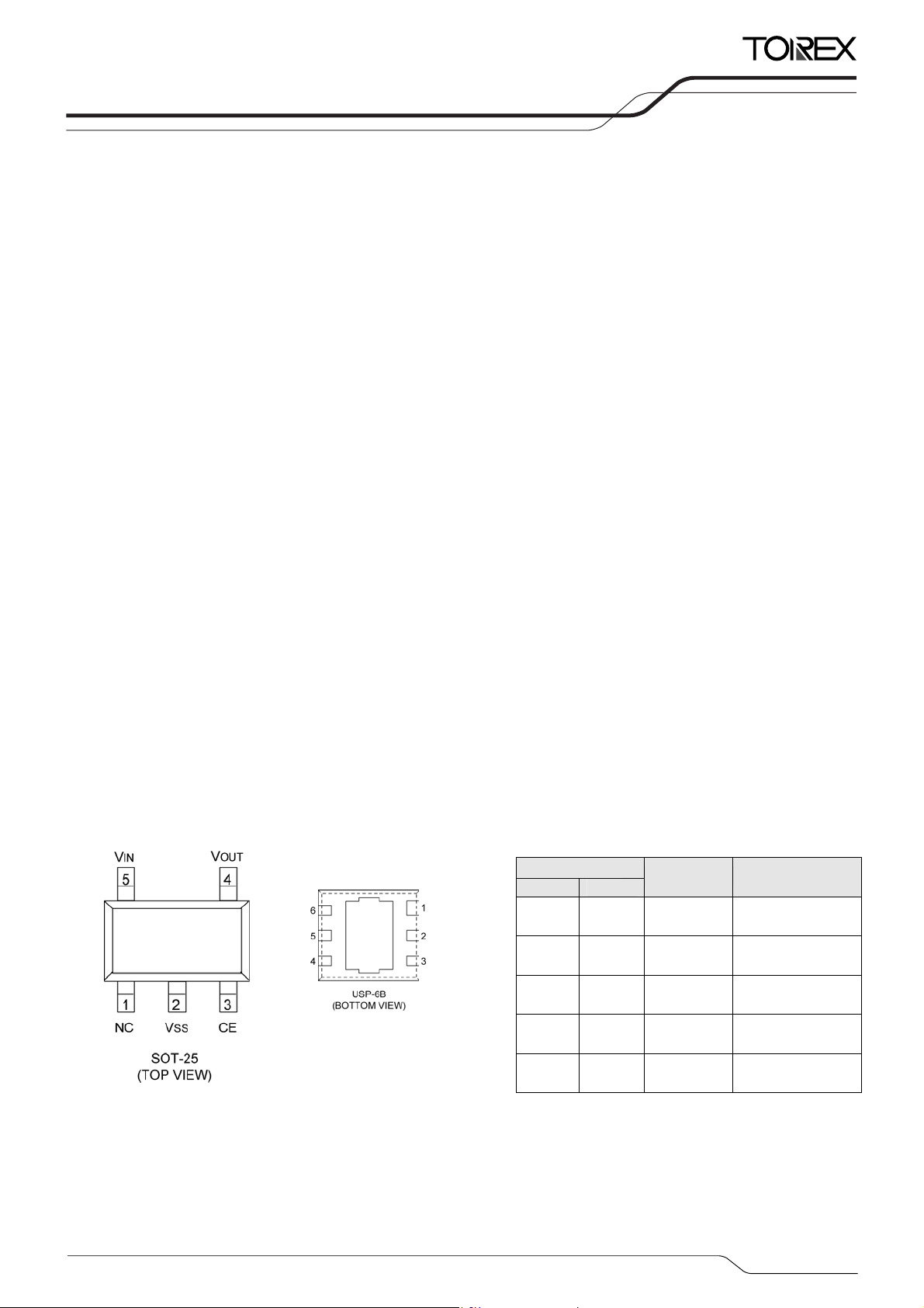
■PIN CONFIGURATION
VSS
NC
CE
*The dissipation pad for the USP-6B
package should be solder-plated in
recommended mount pattern and metal
masking so as to enhance mounting
strength and heat release.
If the pad needs to be connected to other
pins, it should be connected to the V
■FEATURES
Operating Voltage Range : 3.0V ~ 10.0V
Output Voltage Range : 2.0V~ 6.0V
Output Voltage Accuracy : ±3%
Detectable Temperature Range : -30℃ ~ +80℃
Output Voltage Temp. Coefficient : -3900ppm/℃ (TYP.)
Low Power Consumption : 7μA (@V
Packages : SOT-25, USP-6B
Environmentally Friendly : EU RoHS Compliant, Pb Free
OUT=2.0V)
■PIN ASSIGNMENT
VIN
NC
VOUT
SS pin.
PIN NUMBER
SOT-25 USP-6
1 2, 5 NC No Connection
2 6 VSS Ground
3 4 CE Chip Enable
4 3 VOUT Output
5 1 VIN Power Supply
PIN NAME FUNCTION
1/10
A
r
XC31B Series
■PRODUCT CLASSIFICATION
●Ordering Information
XC31B①②③④⑤⑥⑦-⑧
DESIGNATOR DESCRIPTION SYMBOL DESCRIPTION
①
Polarity of Output Voltage
②
③④ Output Voltage (25℃)
⑤
⑥⑦-⑧
(*1)
The “-G” suffix indicates that the products are Halogen and Antimony free as well as being fully RoHS compliant.
(*2)
The device orientation is fixed in its embossed tape pocket. For reverse orientation, please contact your local Torex sales office o
representative. (Standard orientation: ⑥R-⑧ Reverse orientation: ⑥L-⑧)
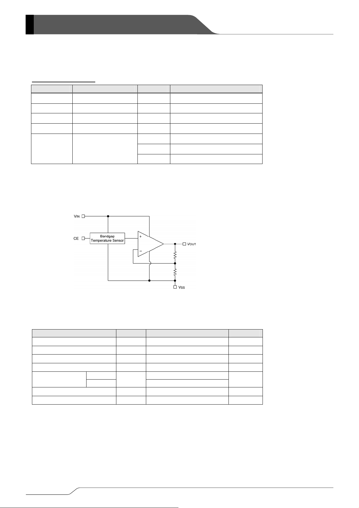
■BLOCK DIAGRAM
BSOLUTE MAXIMUM RATINGS
■
PARAMETER SYMBOL RATINGS UNIT
Input Voltage VIN
Output Voltage VOUT
CE Pin Voltage VCE
Output Current IOUT 20 mA
Power Dissipation
Operating Temperature Range Topr
Storage Temperature Range Tstg
(*1)
P + (Positive)
Temperature Coefficient
N - (Negative)
20~60 e.g. 20=2.0V, 30=3.0V
Revision Character A ~ -
MR SOT-25
Packages
Taping Type
(*2)
MR-G SOT-25
DR USP-6B
Ta=25℃,VSS=0V
-0.3 ~ 12
-0.3 ~ 12
-0.3 ~ V
SOT-25 150
USP-6B
Pd
IN+0.3
100
-30 ~ +80 ℃
-40 ~ +125 ℃
V
V
V
mW
2/10
(T)
■ELECTRICAL CHARACTERISTICS
XC31BPN20A VOUT
(
*1)
=2.0V
PARAMETER SYMBOL CONDITIONS MIN. TYP. MAX. UNITS
Input Voltage VIN
Output Voltage VOUT
Detectable
Temperature Range
Output Voltage
Temperature Coefficient
-30
T
D
Temperature Sensitivity TSE
Linearity Margin Error TL
Load Regulation
(*4)
△VOUT
Supply Current 1 ISS1
Supply Current 2 ISS2
(*3)
OUT=100μA
I
IN=4.0V, VCE=VSS, Ta=25℃
V
(*2)
, VIN=4.0V, Ta=25℃
I
OUT=100μA, VIN=4.0V
-30℃≦Ta≦80℃
-30℃≦Ta≦80℃
-30℃≦Ta≦80℃ -
IN=4.0V
V
1μA≦I
IN=VCE=4.0V, Ta=25℃ -
V
OUT≦100μA
CE "High" Level Voltage VCEH 1.5
CE "Low" Level Voltage VCEL
(*1)
XC31BPN40A VOUT(T)
=4.0V
- -
1.94 2.0 2.06 V
-
+80
-3400 -3900 -4400
-6.8 -7.8 -8.8
1 3.5 %
-
2.0
7 17
-
- -
- -
PARAMETER SYMBOL CONDITIONS MIN. TYP. MAX. UNITS
Input Voltage VIN
Output Voltage VOUT
Detectable
Temperature Range
Output Voltage
Temperature Coefficient
T
D
Temperature Sensitivity TSE
Linearity Margin Error TL
Load Regulation
△V
Supply Current 1 ISS1
Supply Current 2 ISS2
OUT=100μA
I
-30
(*3)
(*4)
OUT
I
V
IN=6.0V, VCE=VSS, Ta=25℃ - -
V
(*2)
, VIN=6.0V,Ta=25℃
OUT=100μA, VIN=6.0V
-30℃≦Ta≦80℃
-30℃≦Ta≦80℃
-30℃≦Ta≦80℃ -
VIN=6.0V
1μA≦I
IN=VCE=6.0V, Ta=25℃ -
OUT≦100μA
CE "High" Level Voltage VCEH 1.5
CE "Low" Level Voltage VCEL
NOTE:
*1: V
OUT(T) =Specified output voltage at 25℃.
*2: When output current exceed 100μA, output voltage drop will increase.
If this IC is to be used in applications where such currents are required, please use a buffer on the output
*3: Output voltage temperature coefficient (T
V
OUT
△
TD=
Ta・V
OUT
*4: Linearity margin error (TL) is calculated as follows:
Tse
emax
・△
Ta
TL=
where emax = maximum error.
The maximum error is the maximum difference between the actual measured value and the value on an approximated straight line.
D) is defined as:
- -
3.88 2.0 4.12 V
-
+80
-3400 -3900 -4400
-13.6 -15.6 -17.6
1 3.5 %
-
3.0
8 18
- -
- -
XC31B
Series
10 V
℃
ppm/℃
mV/℃
-
0.1
0.3 V
10 V
-
0.1
0.3 V
mV
μA
μA
V
℃
ppm/℃
mV/℃
mV
μA
μA
V
3/10

XC31B Series
■TYPICAL APPLICATION CIRCUIT
■NOTE ON USE
1. When the load capacitance CL is too large, oscillation may occur on the output signal.
2. Output signal overshoot will occur when the power (V
enable (CE) function is effective for helping to avoid overshoot and also in saving consumption current.
4/10
IN) is switched on or when the power drastically fluctuates. The chip

■TYPICAL PERFORMANCE CHARACTERISTICS
(1) Output Voltage vs. Ambient Temperature
(2) Supply Current vs. Ambient Temperature
(3) Output Voltage vs. Input Voltage
XC31BPN20A(2.0V) XC31BPN40A(4.0V)
2.1
XC31BPN20A(2.0V) XC31BPN40A(4.0V)
XC31BPN20A(2.0V) XC31BPN40A(4.0V)
XC31B
Series
5/10

XC31B Series
■TYPICAL PERFORMANCE CHARACTERISTICS(Continued)
(4) Input Transient Response 1
(5) Input Transient Response 2
(6) CE Pin Transient Response
6/10

■TYPICAL PERFORMANCE CHARACTERISTICS(Continued)
(7) Ripple Rejection Rate
■PACKAGING INFORMATION
●SOT-25 ●USP-6B
XC31B
Series
7/10

XC31B Series
■PACKAGING INFORMATION (Continued)
●USP-6B Recommended Pattern Layout ●USP-6B Recommended Metal Mask Design
8/10

■MARKING RULE
●SOT-25
SOT-25
(TOP VIEW)
●USP-6B
USP-6B
(TOP VIEW)
① based on internal standards
② represents integer of output voltage
MARK VOLTAGE (V)
2 2.x
3
4
3.x
4.x
5 5.x
6 6.x
③ represents decimal number point of output voltage
MARK VOLTAGE (V)
0 x.0
1
2
x.1
x.2
3 x.3
4 x.4
5 x.5
6 x.6
7 x.7
8 x.8
9 x.9
④ represents assembly lot number
(Based on internal standards)
① represents polarity of output voltage
MARK POLARITY PRODUCT SERIES
P + XC31BPN**AD*
② represents temperature coefficient
MARK COEFFICIENT PRODUCT SERIES
N - XC31BPN**AD*
③④ represents output voltage(25℃)
Ex)
MARK
③ ④
VOLTAGE
(V)
PRODUCT SERIES
2 0 2.0 XC31BPN20AD*
3 0 3.0 XC31BPN30AD*
⑤ represents revision character
Ex)
MARK PRODUCT SERIES
A XC31BPN**AD*
XC31B
Series
⑥ represents production lot number
0~9, A~Z repeated. (G, I, J, O, Q, W excluded)
*No character inversion used.
9/10

XC31B Series
1. The product s and product specifications cont ained herein are subject to change without
notice to improve performance characteristics. Consult us, or our representatives
before use, to confirm that the information in this datasheet is up to date.
2. We assume no responsibility for any infringement of patents, patent rights, or other
rights arising from the use of any information and circuitry in this datasheet.
3. Please ensure suitable shipping controls (including fail-safe designs and aging
protection) are in force for equipment employing products listed in this datasheet.
4. The products in this datasheet are not developed, designed, or approved for use with
such equipment whose failure of malfunction can be reasonably expected to directly
endanger the life of, or cause significant injury to, the user.
(e.g. Atomic energy; aerospace; transport; combustion and associated safety
equipment thereof.)
5. Please use the products listed in this datasheet within the specified ranges.
Should you wish to use the products under conditions exceeding the specifications,
please consult us or our representatives.
6. We assume no responsibility for damage or loss due to abnormal use.
7. All rights reserved. No part of this datasheet may be copied or reproduced without the
prior permission of TOREX SEMICONDUCTOR LTD.
10/10
 Loading...