

■
■
■
XC3101 Series
Ultra Small Analog Output Temperature Sensor with Alarm Output Pin
GENERAL DESCRIPTION
The XC3101 series is a temperature sensor IC which features ultra small, low current consumption, and high-accurate
detection.
It can provide both analog and alarm outputs. The alarm output configures N-channel open-drain. The device consists of a
band-gap type temperature sensor, a voltage reference, a temperature setting tilt amplifier, a comparator, and various set
resistors.
Alarm temperature is internally set at 70℃.
When the temperature exceeds a set point, the alarm output is maintained as "Low".
When the temperature drops a pre-set hysteresis width from the set point, the alarm output is released to "High". The
hysteresis width is 5℃.
An analog voltage output is provided in a high-accuracy which is guaranteed in the operating temperature range of -40℃ to
100℃. An external A/D can monitor the sensing temperature.
The operating input voltage range is 2.7 to 5.5V. The small consumption current of 3.5μA (TYP.) is ideally suited for
temperature detection for battery devices. The ultra small USPN-4 (1.2 x 0.9 x 0.4) package is available for the high-density
board mounting in mobile device applications as well as an industry standard package SSOT-24.
■APPLICATIONS
●
Base temperature monitoring on mobile devices
●
Internal temperature monitoring on small electronic device
● Temperature monitoring (LCD, Module)
● Temperature control for FAN
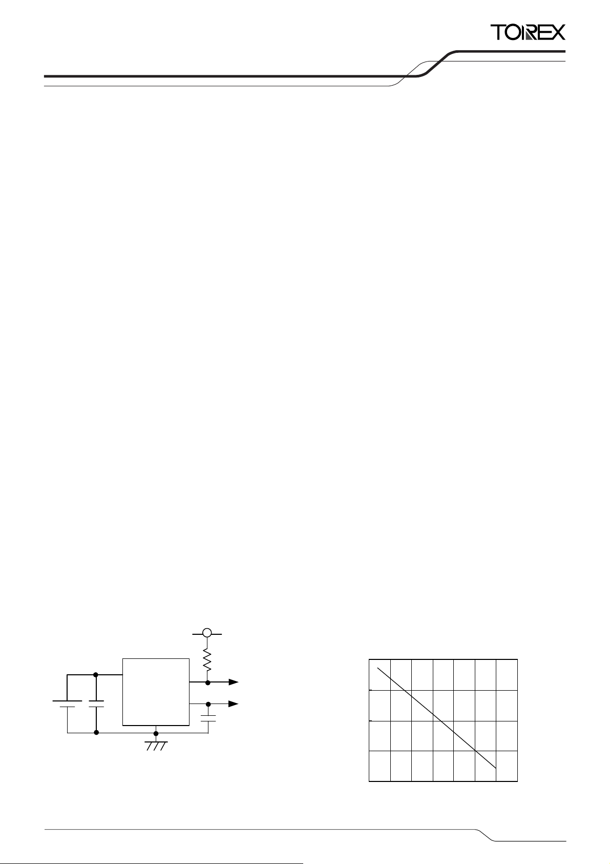
■TYPICAL APPLICATION CIRCUIT
Vpull-up
R
CL
PULL
Alarm Output
Analog Output
V
BAT
CIN
V
DD
V
DOUT
V
AOUT
V
SS
FEATURES
Operating Voltage Range : 2.7V~5.5V
Analog Output Voltage :
Analog Output Temp. Coefficient : -11.77mV/℃(TYP.)
Analog Output Temp. Range : -40℃〜+100℃
Analog Temperature Accuracy : ±3.5℃
Alarm Temperature : 70℃±4.5℃
Alarm Hysteresis : 5℃ (TYP.)
Alarm Output Configuration : N-channel Open-Drain
Alarm Output Logic : Active Low Alarm
Low Power Consumption : 3.5μA (TYP.) @25℃
Packages : USPN-4, SSOT-24
Environmentally Friendly : EU RoHS Compliant, Pb Free
1.600V (TYP.) @25℃
2.365V (TYP.) @-40℃
0.717V (TYP.) @100℃
TYPICAL PERFORMANCE
CHARACTERISTICS
XC3101AC70
VDD=2.7V,I
C
=0.1F(ceramic),CL=0.1uF(ceramic)
2500
[mV]
AOUT
2000
1500
1000
Analog Output Voltage: V
500
-50 -25 0 25 50 75 100 125
IN
Ambient Temperature: Ta [℃]
AOUT
=1uA
ETR0902-004
1/13
XC3101 Series
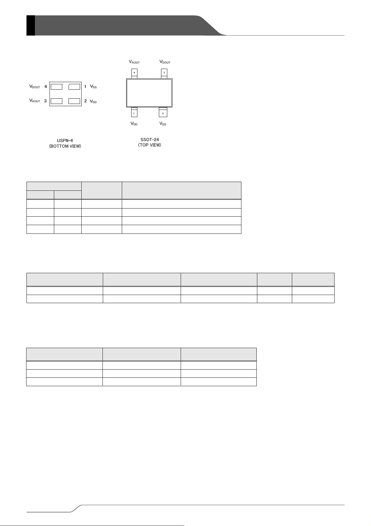
■PIN CONFIGURATION
■PIN ASSIGNMENT
PIN NUMBER
USPN-4 SSOT-24
2 1 VDD Power Supply Input
1 2 VSS Ground
4 3 V
3 4 V
PIN NAME FUNCTIONS
Alarm Output
DOUT
Analog Output
AOUT
PRODUCT CLASSIFICATION
■
●Ordering Information
PRODUCT NAME ALARM TEMPERATURE
XC3101AC70NR-G
XC3101AC707R-G
(*1)
The “-G” suffix indicates that the products are Halogen and Antimony free as well as being fully RoHS compliant.
(*2)
For other alarm temperature besides 70℃, please ask Torex sales contacts.
Optional setting range is 50℃〜95℃.
(*3)
The hysteresis width selections are available in 5℃ and 2 other optional for alarm temperature.
PRODUCT NAME HYSTERESIS WIDTH DESCRIPTION
XC3101AA
XC3101AB
XC3101AC
(*1)
(*1)
70℃ 5℃
70℃ 5℃
0℃ (TYP.)
2.4℃ (TYP.)
5℃ (TYP.)
(*2)
HYSTERESIS WIDTH
Semi-custom
Semi-custom
Standard
(*3)
PACKAGE ORDER UNIT
SSOT-24 3,000/Reel
USPN-4 5,000/Reel
2/13
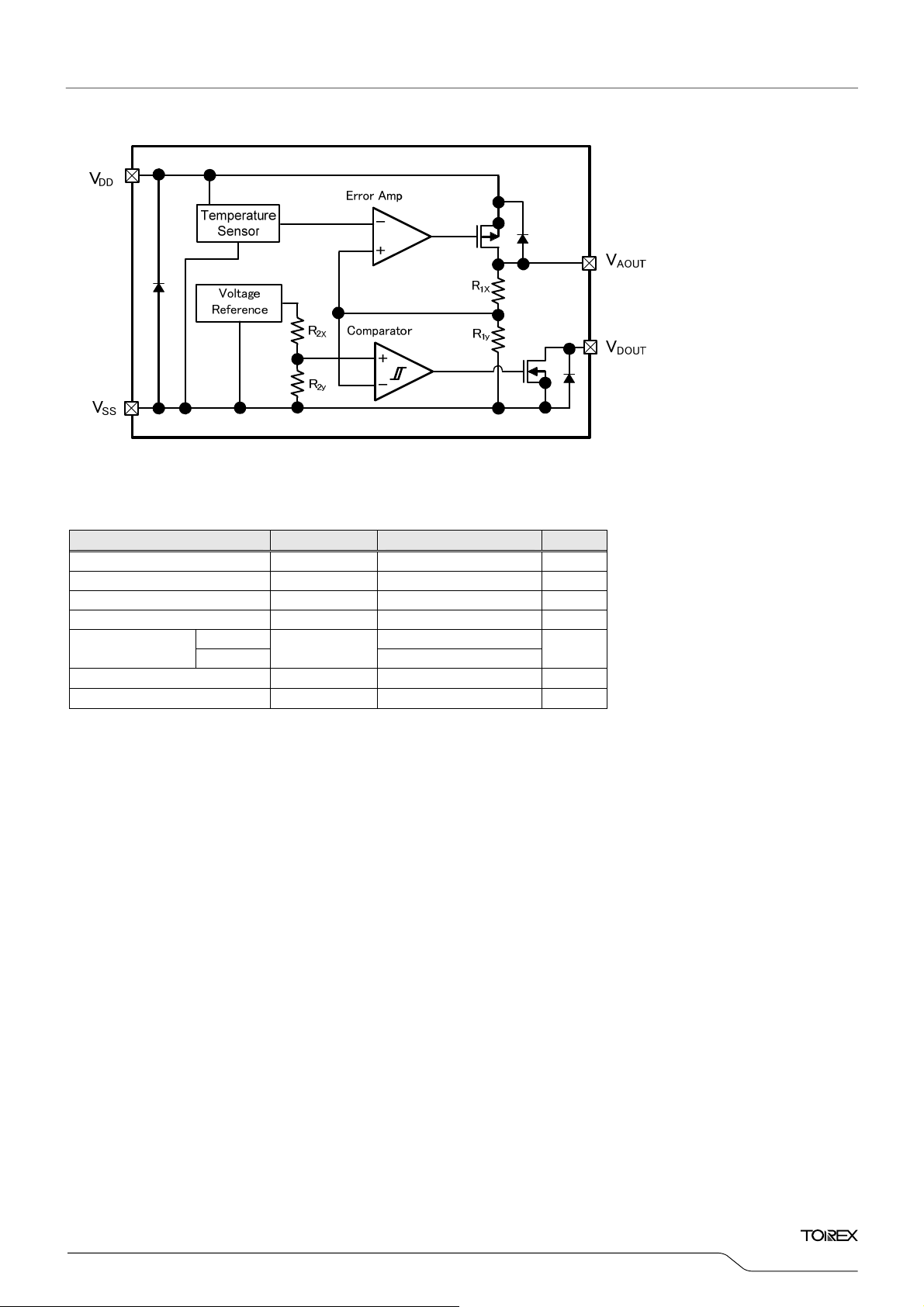
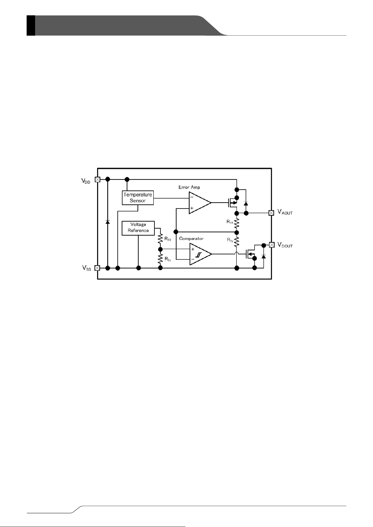
■BLOCK DIAGRAM
*Diodes inside the circuit are an ESD protection diode and a parasitic diode.
XC3101
Series
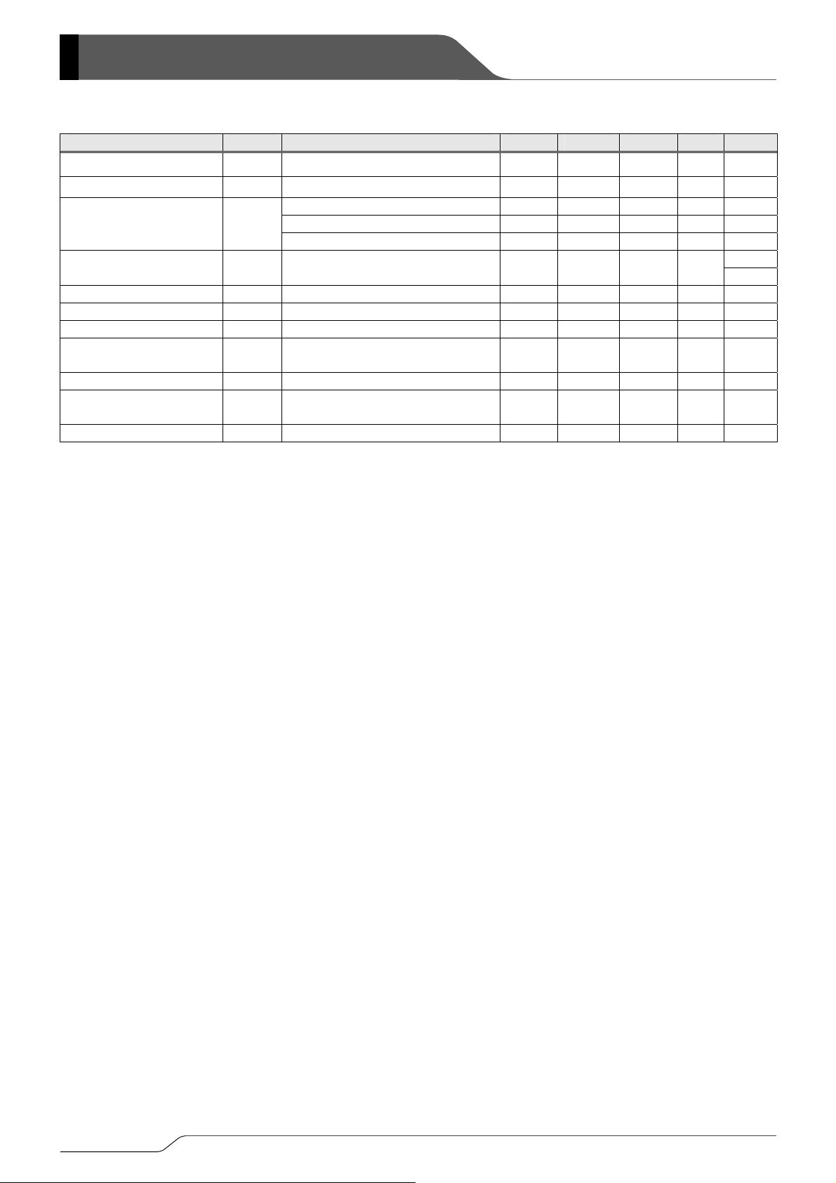
■ABSOLUTE MAXIMUM RATINGS
PARAMETER SYMBOL RATINGS UNITS
Input Voltage VDD V
Analog Output Voltage V
Alarm Output Voltage V
Output Current I
Power Dissipation
Operating Ambient Temperature
Storage Temperature
USPN-4 100
SSOT-24
V
AOUT
V
DOUT
, I
DOUT
30 mA
AOUT
Pd
Ta - 4 0 ~+100 ℃
Ts t g -5 5 ~+125 ℃
SS
-0.3~VDD +0.3 V
SS
SS~VSS
Ta =2 5 ℃
-0.3~+7.0 V
+7.0 V
150
mW
3/13
XC3101 Series
■ELECTRICAL CHARACTERISTICS
XC3101AC70
PARAMETER
SYMBOL
CONDITIONS MIN. TYP. MAX.
Ta =-40℃~100℃
UNITS CIRCUIT
Power Input Range VDD -40℃≦Ta ≦100℃ 2.7 - 5.5 V -
Supply Current
Analog Output Voltage V
Temperature Coefficient
Linearity Margin Error VDD=2.7V~5.5V, I
Load Regulation ΔVO/ΔIO 1μA≦I
Analog Output Current I
Alarm Temperature T
Alarm Temperature Hysteresis Width
Alarm Output Current I
Alarm Output Leakage Current
VDD=3.6V, No load - 3.5 6 μA ②
I
DD
Ta =- 4 0 ℃, VDD=2.7V~5.5V, I
AOUT
d V
AOUT
AOUT
T
DOUT
I
DOUTLEAK
Ta =2 5 ℃, VDD=2.7V~5.5V, I
Ta=100℃, V
/dT
VDD=2.7V~5.5V, I
=2.7V~5.5V, I
DD
=10μA -12.52 -11.77 -11.08
AOUT
=10μA - ±0.4 - % ①
AOUT
≦1mA - 5 10 mV ①
AOUT
VDD=2.7V~5.5V 1 - - mA ①
V
=2.7V~5.5V, I
DD
DET
Change from low temperature to high temperature
VDD=2.7V~5.5V, I
HYS
V
=2.7V ,V
DD
N-ch open drain output
VDD=5.5V, V
DOUT
DOUT
=10μA
AOUT
=10μA T
AOUT
=0.3V , V
=5.5V, V
=10μA 2324 2365 2406 mV ①
AOUT
=10μA 1559 1600 1641 mV ①
AOUT
=10μA 676 717 758 mV ①
AOUT
mV/
℃
65.5 70.0 74.5 ℃ ①
-6.5 T
DET
AOUT=VSS
=2.5V - 0.001 0.2 μA ③
AOUT
1 - - mA ③
DET
-5
T
DET
-3.5
℃ ①
NOTE:
(*1) The value is specified in design values under shipping Inspection at a normal temperature and a high temperature.
(*1)
① Analog Output Voltage
①
4/13

■TEST CIRCUITS
Circuit ①
Circuit ②
Circuit ③
Circuit ④
CIN:0.1uF
CIN:0.1uF
CIN:0.1uF
XC3101
Series
I
AOUT
V
DD
V
SS
V
V
AOUT
DOUT
A
R
:220kΩ
pull
C
:0.1uF
L
V
V
V
DD
V
SS
V
DD
V
SS
V
V
V
V
AOUT
DOUT
AOUT
DOUT
A
A
5/13
XC3101 Series
■OPERATIONAL EXPLANATION
A small ratio of the analog output (V
divider formed by the R1x and R1y resistances. The error amplifier compares this feedback voltage with the voltage of the
internal temperature sensor that is connected to its other input, and the resulting output signal from the error amplifier drives
the Pch-MOS transistor that is connected between the V
via negative feedback. The internal temperature sensor is controlled so that the voltage changes on a fixed temperature
slope with respect to changes of ambient temperature, and a voltage with a fixed temperature slope is thereby output from
the analog output (V
By comparing the internal voltage reference –which has a small temperature slope- with the voltage, divided by R1x and
R
, of the analog output (V
1y
Nch-MOS transistor ON and OFF. Since this Nch-MOS transistor is connected to the V
output voltage (V
<Analog output>
Due to its fixed temperature slope over the temperature range of -40°C to 100°C, the analog output (V
XC3101 series outputs a voltage that varies linearly with changes in ambient temperature. For the XC3101A type, whose
temperature slope is -11.77mV/°C (typical), the analog output voltage at Ta=25°C is 1.6V (typical). The temperature
accuracy by means of the analog output voltage is ±3.5°C.
<Alarm output>
The alarm output (V
temperature rises and the alarm temperature -a threshold set inside the IC- is exceeded. When the ambient temperature
drops below the alarm temperature by an amount that is bigger than the hysteresis width, the alarm output voltage goes
High (pull-up voltage). The alarm output pin is an Nch open drain output, and thus when using alarm output, connect a
pull-up resistor to pull the voltage up to the desired voltage. If not using alarm output, pull the alarm output pin down to the
VSS potential.
<Input/output capacitor>
To stabilize the operation of the XC3101 series, connect a 0.1μF or higher output capacitor (C
pins. To stabilize the input power supply, connect a 0.1μF or higher input capacitor (C
DOUT
).
AOUT
) –which has a fixed temperature slope-, the comparator outputs a voltage that turns the
AOUT
).
) of the XC3101 series holds the alarm output voltage at Low (VSS potential) when the ambient
DOUT
) of the XC3101 series is fed back to one input of the error amplifier via the voltage
AOUT
and V
DD
XC3101 Series
pins. This cycle of events stabilizes the V
AOUT
pin, we actually control the alarm
DOUT
) between the V
L
).
IN
AOUT
AOUT
AOUT
voltage
) of the
and VSS
6/13

XC3101
■NOTES ON USE
1. Please use this IC within the stated maximum ratings. For temporary, transitional voltage drop or voltage rising
phenomenon, the IC is liable to malfunction should the ratings be exceeded.
2. When the wiring impedance is high, noise wraparound due to the output current may cause analog output or alarm
output operation to become unstable. Sufficiently strengthen the V
3. The input capacitor CIN and the output capacitor CL should be placed to the as close as possible with a shorter wiring.
4. Do not use the XC3101 series with a voltage lower than VSS applied to the alarm output pin (V
5. If VIN changes sharply, the analog output will also change sharply, and malfunctioning of the alarm output may result. In
this event, adjust the slew-rate to less than 2 V/ms by increasing the input capacitor (C
6. Torex places an importance on improving our products and its reliability.
However, by any possibility, we would request user fail-safe design and post-aging treatment on system or equipment.
and GND wiring.
DD
).
DOUT
) or other means.
IN
Series
7/13

XC3101 Series
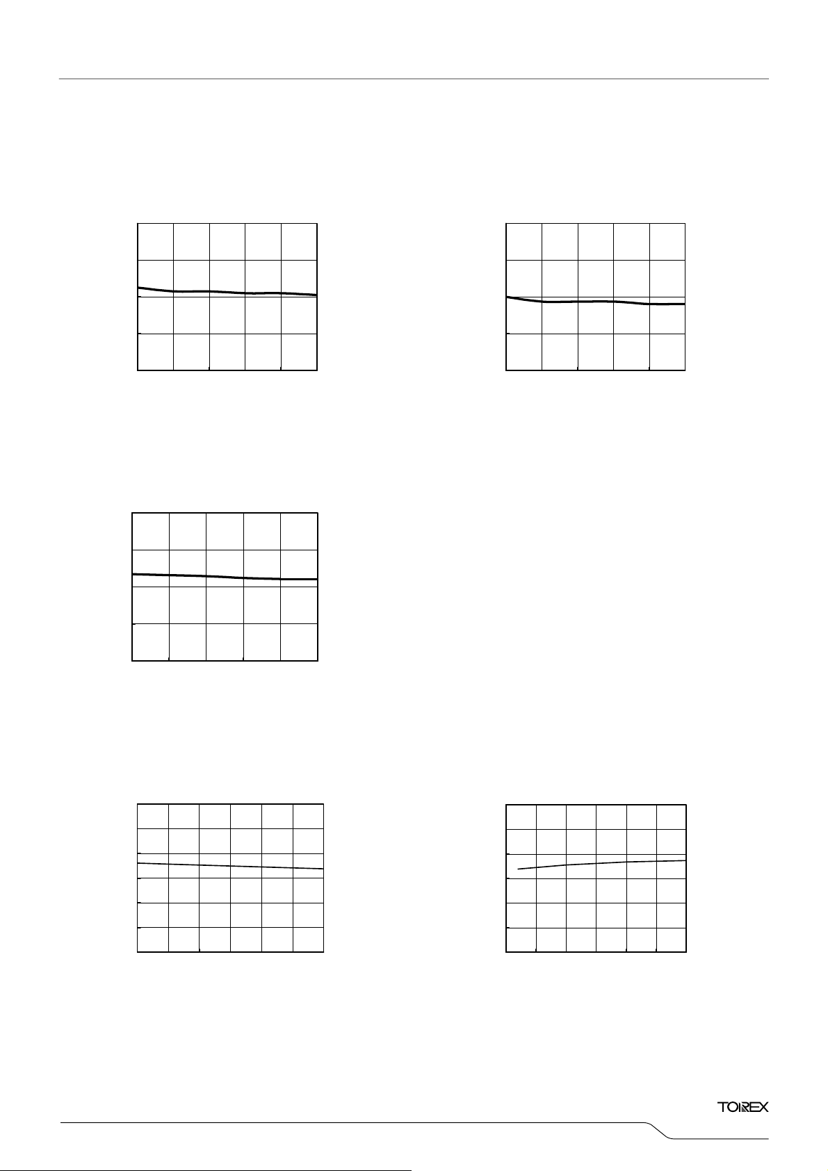
■TYPICAL PERFORMANCE CHARACTERISTICS
(1)Supply Current vs. Ambient Temperature (2)Analog Output Voltage vs. Ambient Temperature
5.0
4.5
[μA]
DD
4.0
3.5
3.0
2.5
Supply Current: I
2.0
-50 -25 0 25 50 75 100 125
(3)Analog Output Temperature Error vs. Ambient Temperature (4)Linearity Margin Error vs. Ambient Temperature
4.0
2.0
0.0
-2.0
Analog Output Temperature Error [℃]
-4.0
-50 -25 0 25 50 75 100 125
(5) Alarm Output Voltage vs. Ambient Temperature
C
IN
0.7
[V]
0.6
DOUT
0.5
0.4
0.3
0.2
0.1
Alarm Output Voltage: V
0
60 62 64 66 68 70 72 74 76
XC3101AC70
VDD=5.5V
VDD=3.6V
Ambient Temperature: Ta [℃]
XC3101AC70
C
=0.1F(ceramic),CL=0.1uF(ceramic)
IN
Ambient Temperature: Ta [℃]
VDD=2.7V,I
AOUT
=1uA
XC3101AC70
=0.1F(ceramic),CL=0.1uF(ceramic),Rpull=220k
VDD=2.7V,I
Ambient Temperature: Ta [℃]
=1uA,Vpull-up=0.5V
AOUT
XC3101AC70
C
=0.1F(ceramic),CL=0.1uF(ceramic)
2500
[mV]
AOUT
2000
1500
1000
Analog Output Voltage: V
500
-50 -25 0 25 50 75 100 125
IN
Ambient Temperature: Ta [℃]
VDD=2.7V,I
XC3101AC70
C
=0.1F(ceramic),CL=0.1uF(ceramic)
0.4
0.3
0.2
0.1
-0.1
-0.2
Linearity Margin Error [%]
-0.3
-0.4
0
IN
-50 -25 0 25 50 75 100 125
Ambient Temperature: Ta [℃]
VDD=2.7V,I
AOUT
AOUT
=1uA
=1uA
8/13
■TYPICAL PERFORMANCE CHARACTERISTICS (Continued)
(6) Analog Output Voltage vs. Analog Output Current
2400
[mV]
AOUT
2380
XC3101AC70
C
=0.1F(ceramic),CL=0.1uF(ceramic)
IN
Ta=-40℃,VDD=2.7V
[mV]
AOUT
1640
1620
2360
1600
2340
1580
2320
Analog Output Voltage :V
0 0.3 0.6 0.9 1.2 1.5
Analog Output Current :I
AOUT
[mA]
Analog Output Voltage :V
1560
800
[mV]
AOUT
750
XC3101AC70
C
=0.1F(ceramic),CL=0.1uF(ceramic)
IN
Ta=100℃,VDD=2.7V
700
650
600
Analog Output Voltage :V
0 0.3 0.6 0.9 1.2 1.5
Analog Output Current :I
AOUT
[mA]
(7) Alarm Output Current vs. Ambient Temperature (8) Alarm Output Current vs. Input Voltage
6.0
[mA]
5.0
DOUT
4.0
3.0
2.0
1.0
Alarm Output Current: I
0.0
70 80 90 100
XC3101AC70
VDD=2.7V,V
CIN=0.1F(ceramic),CL=0.1uF(ceramic)
Ambient Temperature: Ta [℃]
DOUT
=0.3V,V
AOUT=VSS
6.0
[mA]
5.0
DOUT
4.0
3.0
2.0
1.0
Alarm Output Current: I
0.0
2.5 3 3.5 4 4.5 5 5.5
XC3101AC70
C
=0.1F(ceramic),CL=0.1uF(ceramic)
IN
0 0.3 0.6 0.9 1.2 1.5
Analog Output Current :I
Ta=25℃,VDD=2.7V
[mA]
AOUT
XC3101AC70
Ta=100℃,V
CIN=0.1F(ceramic),CL=0.1uF(ceramic)
Input Voltage: V
DOUT
=0.3V,V
[V]
DD
AOUT=VSS
XC3101
Series
9/13

XC3101 Series
■PACKAGING INFORMATION
●SSOT-24
Unit: mm
+0.15
0.25
-0.1
+0.15
0.25
-0.1
●USPN-4
Unit: mm
1.2±0.05
+0.02
-0.03
0.38
C0.
05
2.0±0.1
1.3±0.2
0.9±0.05
1pin INDENT
0.2±0.05
12
43
(0.55)
0.25±0.05
0.35
0.05
0.425±0.05
0.25
+0.15
-0.1
+0.15
-0.1
+0.1
0.125
-0.05
USPN-4 Package
0
+0.1
-0
10/13

■PACKAGING INFORMATION (Continued)
●USPN-4 Reference Pattern Layout ●USPN-4 Reference Metal Mask Design
Unit: mm
C0.
0.25 0.25
4
075
0.125 0.55 0.125
1
3
2
0.2 0.2
4
C0.0
5
1
0.1 0.10.55
3
2
XC3101
Series
11/13

XC3101 Series
■MARKING RULE
●SSOT-24
(With the orientation bar at the bottom)
(方向下バー付きタイプ)
4
* SSOT-24 has the orientation bar marked in the bottom.
②①
3
④
③
0〜0, A〜Z are in an order.
1
2
●USPN-4
1
2
①②
④⑤③
4
3
01〜09, 0A〜0Z, 11〜9Z, A1〜A9, AA〜AZ, B1〜ZZ are in an order.
(G, I, J, O, Q, W excluded.)
① represents product series
MARK PRODUCT SERIES
N XC3101******-G
② represents production registered number
(G, I, J, O, Q, W excluded.)
* No character inversion used.
③④ represents production lot number.
01~09, 0A~0Z, 11~9Z, A1~A9, AA〜AZ、B1〜ZZ repeated.
(G, I, J, O, Q, W excluded.)
* No character inversion used.
① represents product series
MARK PRODUCT SERIES
D XC3101******-G
②③ represents production registered number
* No character inversion used.
④⑤ represents production lot number.
01~09, 0A~0Z, 11~9Z, A1~A9, AA〜AZ、B1〜ZZ repeated.
(G, I, J, O, Q, W excluded.)
* No character inversion used.
12/13

XC3101
Series
1. The products and product specifications contained herein are subject to change without
notice to improve performance characteristics. Consult us, or our representatives
before use, to confirm that the information in this datasheet is up to date.
2. We assume no responsibility for any infringement of patents, patent rights, or other
rights arising from the use of any information and circuitry in this datasheet.
3. Please ensure suitable shipping controls (including fail-safe designs and aging
protection) are in force for equipment employing products listed in this datasheet.
4. The products in this datasheet are not developed, designed, or approved for use with
such equipment whose failure of malfunction can be reasonably expected to directly
endanger the life of, or cause significant injury to, the user.
(e.g. Atomic energy; aerospace; transport; combustion and associated safety
equipment thereof.)
5. Please use the products listed in this datasheet within the specified ranges.
Should you wish to use the products under conditions exceeding the specifications,
please consult us or our representatives.
6. We assume no responsibility for damage or loss due to abnormal use.
7. All rights reserved. No part of this datasheet may be copied or reproduced without the
prior permission of TOREX SEMICONDUCTOR LTD.
13/13
 Loading...