

XC25BS8 Series
ETR1506-007a
Ultra Small PLL Clock Generator ICs with Built-In Divider/Multiplier Circuits
■GENERAL DESCRIPTION
The XC25BS8 series is an ultra small PLL clock generator IC which can generate a high multiplier output up to 4095 from an input frequency as
low as 8kHz. The series includes a divider circuit, phase/frequency comparator, charge pump, and VCO so it is possible to configure a fully
operational circuit with a few external components like one low-pass filter capacitor. The Input divider ratio (M) can be selected from a range of 1
to 2047, the output divider ratio (N) can be selected from a range of 1 to 4095 and they are set internally by using laser timing technologies.
Output frequency (fQ0) is equal to input clock frequency (f
from 8kHz to 36MHz can be input as the input clock. The IC stops operation and current drain is suppressed when a low level signal is input to the
CE pin which greatly reduces current consumption and produces a high impedance output.
The setting of the input divider ratio (M), output divider ratio (N), and charge pump current (Ip) are factory fixed semi-custom. Please advise your
Torex sales representative of your particular input/output frequency and supply voltage specifications so that we can see if we will be able to
support your requirements. The series is available in small SOT-26W and USP-6C.
■ APPLICATIONS
● Clock for controlling a Imaging dot (LCD)
● DSC (Digital still camera)
● DVC (Digital video camera)
● PND (Car navigation system)
● UMPC (Ultra Mobile Personal Computer)
● SSD (Solid State Disk)
● Digital Photo Frame
● Microcomputer and HDD drives
● Cordless phones & Wireless communication
equipment
● Various system clocks
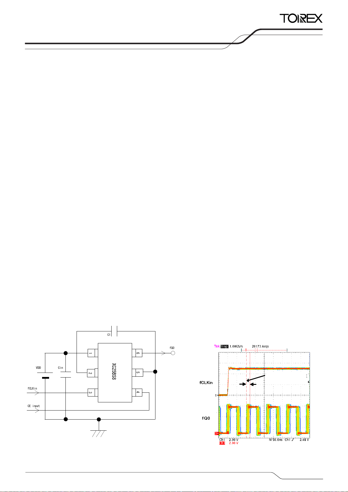
■TYPICAL APPLICATION CIRCUIT
) multiplied by N/M. Output frequency range is 1MHz to 100MHz. Reference clock
CLKin
■FEATURES
× N/M)
(*1)
(*1)
(*1)
(*1)
(*1)
Input Frequency Range : 8kHz ~ 36MHz
Output Frequency Range : 1MHz ~ 100MHz
(fQ0=f
CLKin
Output Divider (N) Range : 1 ~ 4095
Input Divider (M) Range : 1 ~ 2047
Operating Voltage Range : 2.50V ~ 5.50V
Low Power Consumption : 10μA MAX. when stand-by
Small Packages : SOT-26W, USP-6C
*1: The series are semi-custom products. Specifications for each
product are limited within the above range. The input frequency
range is set within ±5% of customer’s designated typical frequency.
Please note that setting of your some requirements may not be
possible due to the specification limits of this series.
*2: When the IC is in stand-by mode, the output becomes high impedance
and the IC stops operation.
■ TYPICAL PERFORMANCE
CHARACTERISTICS
PLL Output signal jitter 2 (tJ2) (synchronous to an input signal)
XC25BS8001xx (610 multiplier, input 15kHz (TYP.))
(*2)
*1
*1: CIN (by-pass capacitor, 0.1μF) and C1 ( LPF capacitor, 0.1μ
F) should be connected as close as possible to the IC. Please
refer to the pattern reference layout schematics on page 8 for
details.
Input Signal
Output Signal
Output jitter
t
=20(ns)
J2
1/14
XC25BS8Series
■PIN CONFIGURATION
■PIN ASSIGNEMNT
PIN NUMBER
SOT-26W USP-6C
6 1 Q0 Clock Output
5 2 VSS Ground
4 3 CE
3 4 CLKin Reference Clock Signal Input
2 5 LPF Device connection for Low Pass Filter
1 6 VDD Power Input
■ FUNCTION LIST
CE 'H'' 'L'' or OPEN
Q0 Signal Output High Impedance
Q0
V
6
132
DD
SOT-26W
(TOP VIEW)
V
SS
LPF
CE
45
CLKin
PIN NAME
V
DD
LPF
CLKin
6
5
4
USP-6C
(BOTTOM VIEW)
Stand-by Control
1
2
3
FUNCTION
Q0
V
SS
CE
(*)
*H: High level input
L: Low level input (stand-by mode)
* The dissipation pad (TAB) of the
bottom view of the USP-6C package
should be connected to the V
pin.
(No. 2)
SS
2/14
■ PRODUCT CLASSIFICATION
●Ordering Information
XC25BS8①②③④⑤-⑥
(*1)
DESIGNATOR DESCRIPTION SYMBOL DESCRIPTION
XC25BS8
Series
①②③
Product Number 001~
Serial number based on internal standards
e.g. product number 001→①②③=001
MR SOT-26W
④⑤-⑥
Packages
Taping Type
(*2)
MR-G SOT-26W (Halogen & Antimony free)
ER USP-6C
ER-G USP-6C (Halogen & Antimony free)
(*1)
The “-G” suffix indicates that the products are Halogen and Antimony free as well as being fully RoHS compliant.
(*2)
The device orientation is fixed in its embossed tape pocket. For reverse orientation, please contact your local Torex sales office or
representative. (Standard orientation: ④R-⑥, Reverse orientation: ④L-⑥)
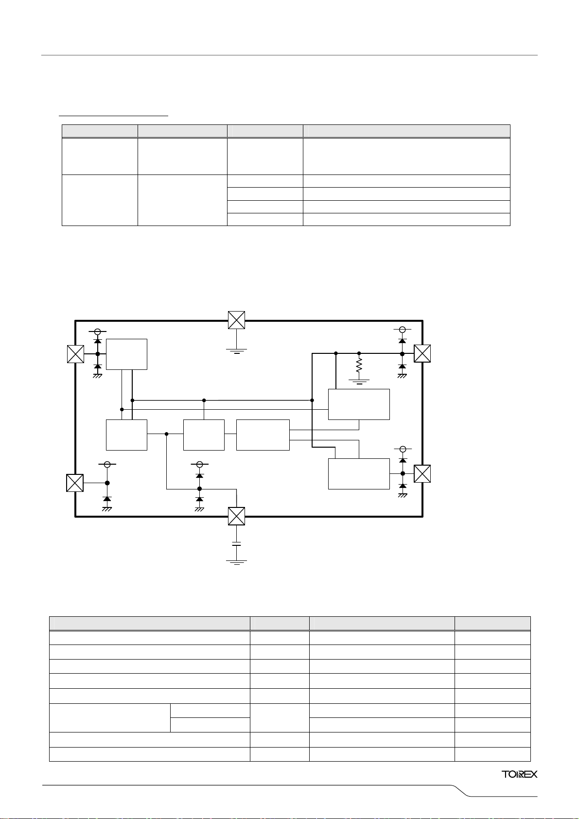
■BLOCK DIAGRAM
Q
0
Output
Buffer
V
SS
CE
Rdn
1/N
Counter
VCO
Charge
Pump
Phase
Detector
V
DD
LPF
C1
■ABSOLUTE MAXIMUM RATINGS
PARAMETER SYMBOL RATINGS UNITS
Supply Voltage VDD
CLKin Pin Input Voltage VCK
CE Pin Input Voltage VCE
Q0 Pin Output Voltage VQ0
Q0 Pin Output Current IQ0 ± 50 mA
Power Dissipation
SOT-26W
USP-6C
Operating Temperature Range Topr
Storage Temperature Range Tstg
1/M
Counter
C1:Low Pass Filter Ceramic Capacitor
(Please set as an external components between LPF Pin and V
Recommended components (1608 Type);
C1:0.1μF ---- Taiyo yuden EMK107BJ104KA
- 0.3 ~ VSS + 7.0
V
SS
- 0.3 ~ VDD + 0.3
V
SS
- 0.3 ~ VDD + 0.3
V
SS
- 0.3 ~ VDD + 0.3
V
SS
Pd
250
CLK
in
100
-40 ~+85 ℃
-55 ~+125 ℃
V
V
V
V
mW
mW
)
SS
Ta =2 5 ℃
3/14
XC25BS8Series
■ SELECTION GUIDE
*1: The table below introduces standard products. Please select with seeing the combination of input frequencies and multiplications.
The test condition: V
*2:
For other input frequency and multiplication, please ask your Torex sales contacts.
Multiplication
64 32kHz ~ 192kHz 36ns 10% XC25BS8044
128
192
256
384
512
768
* Synchronization jitters are tested at f
Multiplication
64 8kHz ~ 16kHz 160ns 8% XC25BS8045
128 8kHz ~ 16kHz 140ns 14% XC25BS8029
192 8kHz ~ 16kHz 110ns 17% XC25BS8032
256 8kHz ~ 16kHz 100ns 20% XC25BS8034
384 8kHz ~ 16kHz 96ns 29% XC25BS8038
512 8kHz ~ 16kHz 52ns 21% XC25BS8041
768 8kHz ~ 16kHz 48ns 29% XC25BS8046
* Synchronization jitters are tested at f
Multiplication
1
2
3
4
5
6
7
8
9
10
* Synchronization jitters are tested in the condition below.
For the XC258047 (1 Multiplication), f
Except above, f
=3.3V±10%
DD
Input Frequency
MIN ~ MAX
Synchronization
jitter
Synchronization
jitter
/ Output Period (%)
Product Series
32kHz ~ 192kHz 32ns 18% XC25BS8027
32kHz ~ 96kHz 24ns 14% XC25BS8028
32kHz ~ 48kHz 20ns 11% XC25BS8057
32kHz ~ 192kHz 30ns 25% XC25BS8030
32kHz ~ 96kHz 20ns 17% XC25BS8031
32kHz ~ 48kHz 16ns 14% XC25BS8058
32kHz ~ 192kHz 24ns 27% XC25BS8033
32kHz ~ 96kHz 22ns 25% XC25BS8026
32kHz ~ 48kHz 18ns 20% XC25BS8025
32kHz ~ 192kHz 21ns 36% XC25BS8035
32kHz ~ 96kHz 20ns 34% XC25BS8036
32kHz ~ 48kHz 18ns 30% XC25BS8037
32kHz ~ 96kHz 18ns 41% XC25BS8039
32kHz ~ 48kHz 16ns 36% XC25BS8040
32kHz ~ 96kHz 16ns 54% XC25BS8042
32kHz ~ 48kHz 14ns 47% XC25BS8043
=44.1kHz.
CLKIN
Input Frequency
MIN ~ MAX
=8kH.
CLKIN
Input Frequency
MIN ~ MAX
8MHz
6MHz
2MHz
2MHz
2MHz
2MHz
2MHz
2MHz
2MHz
2MHz
=3MHz is used.
CLKIN
74MHz 7ns 8%
~
37MHz 6ns 11%
~
24MHz 12ns 11%
~
18MHz 7ns 8%
~
14MHz 8ns 12%
~
12MHz 7ns 13%
~
10MHz 7ns 15%
~
9MHz 6ns 14%
~
8MHz 6ns 16%
~
7MHz 7ns 21%
~
=12MHz. For the XC258048(2 Multiplication), f
CLKIN
Amount of Jitter
Synchronization
Amount of Jitter
Synchronization
Amount of Jitter
Synchronization
/ Output Period (%)
Amount of Jitter
Synchronization
/ Output Period (%)
= 8MHz
CLKIN
Product Series
Product Series
XC25BS8047
XC25BS8048
XC25BS8049
XC25BS8050
XC25BS8051
XC25BS8052
XC25BS8053
XC25BS8054
XC25BS8055
XC25BS8056
4/14
XC25BS8
■ELECTRICAL CHARACTERISTICS
●Recommended Operating Conditions: XC25BS8050xx (4 multiplication, Input 3MHz (TYP.)) 3.3V (TYP.)
PARAMETER SYMBOL CONDITIONS MIN. MAX. UNITS
Supply Voltage 3.3V
Input Frequency
Multiplier Ratio
Output Frequency
Load Capacity
Output Start Time
NOTE:
*1: The values are measured when a capacitor C
between LFP and V
*2: It is a time to get stable output signal from Q0 pin after the CE pin is turned on while applying supply voltage to the V
input signal to the CLKin pin.
*3: Values indicated are design values which are not guaranteed 100%.
●DC Characteristics: XC25BS8050xx (4 multiplication, Input 3MHz (TYP.)) 3.3V (TYP.)
(*3)
CL
(*2)(*3)
pins
SS
VDD
f
CLKin
N/M
fQ0
t
START
3.3V (TYP.) operation
(*1)
Typical value is shown
(*1)
=0.1μF is connected between VDD and V
IN
=2.000MHz
f
CLKin
(*1)
2.97 3.63 V
2.000 18.500 MHz
4 -
8.000 74.000 MHz
- 15 pF
0.05 20 ms
pins, a capacitor C1=0.1μF is connected
SS
PARAMETER SYMBOL CONDITIONS MIN. TYP. MAX. UNITS CIRCUIT
H Level Input Voltage VIH 2.70 - - V
L Level Input Voltage VIL - - 0.60 V
H Level Input Current
L Level Input Current
H Level Output Voltage
L Level Output Voltage
Supply Current 1
Supply Current 2
CE H Level Voltage
CE L Level Voltage
CE Pull-Down Resistance 1
CE Pull-Down Resistance 2
Output Off Leak Current
NOTE:
TEST CONDITION: V
●AC Characteristics: XC25BS8050xx (4 multiplication, 3MHz(TYP.)) 3.3V (TYP.)
=3.0V, f
DD
IiH V
CLKin=VDD
IiL V
VOH
VOL
I
DD1
I
DD2
V
2.70 - - V
CEH
V
- - 0.45 V
CEL
=2.97V,IOH=-4mA
V
DD
=2.97V,IOL= 4mA
V
DD
=3.63V,CE= 3.63V
V
DD
=3.63V,CE= 0.0V
V
DD
Rdn1 CE= V
Rdn2 CE= 0.1*V
I
OZ
=3MHz, C1=0.1μF, Multiplier ratio=4, No load
CLKin
=3.63V,CE= 0.0V
V
DD
-0.3V - - 3.0
=0.3V -3.0 - -
CLKin
0.1 0.6 1.2
DD
DD
2.38 - - V
- - 0.45 V
- 5.0 10.0 mA
- - 10
5 30 60
- - 10
PARAMETER SYMBOL CONDITIONS MIN. TYP. MAX. UNITS CIRCUIT
Output Rise Time
Output Fall Time
Output Signal Duty Cycle
PLL Output Signal Jitter 1
PLL Output Signal Jitter 2
NOTE:
TEST CONDITION: V
*1: Values indicated are design values, which are not guaranteed 100%.
(*1)
t
(*1)
t
(*1)
(*1)
(*1)
=3.3V, f
DD
R
F
Duty
tJ1
t
J
2
=3MHz, C1=0.1μF, Multiplier ratio=4, CL=15pF
CLKin
(20% ~ 80%) - 4.0 8.0 ns
(20% ~ 80%) - 4.0 8.0 ns
45 50 55
1σ (Output Period)
Peak to Peak (Output Tracking) - 8.0 - ns
- 45 - ps
Tested below Ta=25OC
pin and applying the
DD
μA ②
μA ②
μA ④
MΩ ⑤
kΩ ⑤
μA ⑥
% ①
Series
Ta =2 5 ℃
①
①
③
③
④
①
①
Ta =2 5 ℃
①
①
①
①
5/14

XC25BS8Series
■ELECTRICAL CHARACTERISTICS (Continued)
●Recommended Operating Conditions: XC25BS8025xx (256multiplication, Input 44.1kHz (TYP.)) 5.0V (TYP.)
PARAMETER SYMBOL CONDITIONS MIN. MAX. UNITS
Supply Voltage 5.0V VDD 5.0V (TYP.) operation
Input Frequency f
CLKin
Multiplier Ratio N/M Typical value is shown
Output Frequency fQ0
Load Capacity
Output Start Time
NOTE:
*1: The values are measured when a capacitor C
between LFP and V
*2: It is a time to get stable output signal from Q0 pin after the CE pin is turned on while applying supply voltage to the V
the input signal to the CLKin pin.
*3: Values indicated are design values which are not guaranteed 100%.
●DC Characteristics: XC25BS8025xx (256 multiplication, Input 44.1kHz (TYP.) ) 5.0V (TYP.)
(*3)
CL
(*2)(*3)
SS
pins.
t
START
f
=0.1μF is connected between VDD and V
IN
(*1)
(*1)
=32.000kHz
CLKin
(*1)
4.50 5.50
32.000 48.000 kHz
256
8.693 96.075
- 15
0.05 20 ms
pins, a capacitor C1=0.1μF is connected
SS
PARAMETER SYMBOL CONDITIONS MIN. TYP. MAX. UNITS CIRCUIT
H Level Input Voltage VIH 4.00 - - V
L Level Input Voltage VIL - - 1.00 V
H Level Input Current IIH V
CLKin=VDD
L Level Input Current IIL V
H Level Output Voltage VOH
L Level Output Voltage VOL
Supply Current 1 I
Supply Current 2 I
CE H Level Voltage V
CE L Level Voltage V
DD1
DD2
CEH
CEL
4.00 - - V
- - 1.00 V
=4.50V,IOH=-8mA
V
DD
=4.50V,IOL= 8mA
V
DD
=5.50V,CE= 5.50V
V
DD
=5.50V,CE= 0.0V
V
DD
-0.5V - - 5.0
=0.5V -5.0 - -
CLKin
3.60 - - V
- - 0.65 V
- 6.5 13.0 mA
- - 20
CE Pull-Down Resistance 1 Rdn1 CE= VDD 0.1 0.4 0.8 MΩ
CE Pull-Down Resistance 2 Rdn2 CE= 0.1*VDD 2 20 40 kΩ
Output Off Leak Current IOZ
NOTE:
TEST CONDITION: V
●AC Characteristics: XC25BS8025xx (256 multiplication, Input 44.1kHz (TYP.)) 5.0V (TYP.)
=5.0V, f
DD
=44.1kHz, C1=0.1μF, Multiplier ratio=256, No load
CLKin
=5.50V,CE= 0.0V
V
DD
- - 10
PARAMETER SYMBOL CONDITIONS MIN. TYP. MAX. UNITS CIRCUIT
Output Rise Time
Output Fall Time
Output Signal Duty Cycle
PLL Output Signal Jitter 1
PLL Output Signal Jitter 2
NOTE:
TEST CONDITION: V
*1: Values indicated are design values, which are not guaranteed 100%.
(*1)
t
(*1)
t
(*1)
Duty
(*1)
tJ1
(*1)
=5.0V, fCLKin=44.1kHz, C1=0.1μF, Multiplier ratio=256, CL=15pF
DD
(20% ~ 80%) - 2.5 5.0 ns
R
(20% ~ 80%) - 2.5 5.0 ns
F
1σ (Output Period)
Peak to Peak (Output Tracking) - 18.0 - ns
t
J
2
45 50 55
- 20 - ps
Tested below Ta=25OC
pin and applying
DD
μA ②
μA ②
μA ④
μA ⑥
% ①
V
MHz
pF
Ta =2 5 ℃
①
①
③
③
④
①
①
⑤
⑤
Ta =2 5 ℃
①
①
①
①
6/14

p
XC25BS8
■NOTE ON USE
(1) Please use this IC within the stated absolute maximum ratings. The IC is liable to malfunction should the ratings be
exceeded.
(2) The series is an analog IC. Please use a 0.01μF to 0.1μF of a by-pass capacitor.
(3) The constant of the LPF element of this IC is preset. Always use the capacitance value (=0.1μF) specified by us for
the external ceramic capacitor (C1) for LPF. Operating this IC with a capacitor of the wrong capacitance will cause
erroneous operation.
(4) Rq0 shown in the Typical Application Circuit is a matching resistor. The use is recommended in order to counter
unwanted radiations.
(5) Please place the by-pass capacitor and the matching resistor as close to the IC as possible. The IC may not operate
normally if the by-pass capacitor is not close enough to the IC. Further, the unwanted radiation may occur between
the resistor and the IC pin if the matching resistor is not close enough to the IC.
(6)When the CE pin is not controlled by external signals, it is recommended that a time constant circuit of R1=1kΩ ×C2
= 0.1μF be added for stability.
(7) With this IC, output is achieved by dividing and multiplying the reference oscillation by means of the PLL circuit. In
cases where this output is further used as a reference oscillation of another PLL circuit, it may be that the final output
signal's jitter increases; therefore, all necessary precautions should be taken to avoid this.
(8) It is recommended that a low noise power supply, such as a series regulator, be used as the series’ supply voltage.
Using a power supply such as a switching regulator may enlarge the jitter, which in turn may lead to abnormal
operation. Please confirm its operation with the actual device.
(9) For operating the IC normally, please take procedures below when applying voltage to the series’ input pin:
1) Apply power source while the CE pin is "L" level with no clock input (high-Impedance or “L”),
2) Input the clock,
3) At least 100μs after applying clock input, change the CE pin into “H” level and then to enable.
The IC has to be started by inputting the clock once the power rises completely. The CE pin, then, should be enabling.
If the CE pin becomes enable and the clock is inputted before the power rises completely, an internal reset circuit
does not o
erate normally which may cause to generate extraneous frequency.
●eg.)Matching Resistance (Rq0) and Device for Time constant circuit (R1,C2)are connected,
(Package: SOT-26W)
Series
7/14

XC25BS8Series
■NOTE ON USE (Continued)
●Instructions on Pattern Layout
8/14
In order to stabilize VDD voltage level, we recommend that a by-pass capacitor (CIN) be connected as close as possible to
1.
the V
2. Please mount the low pass filter capacitor C1(=0.1μF) as close to the IC as possible.
3. Make the pattern as close to the IC as possible and use thick, short connecting traces to reduce the circuit impedance.
4. Make sure that the V
result in instability of this product.
< Reference pattern layout >
and VSS pins.
DD
(GND) traces are as thick as possible, as variations in ground potential caused by noise may
SS
* We prepare the evaluation board PCB, which is designed by the below layout pattern.
1. SOT-26W Reference Pattern Layout
2. USP-6C Reference Pattern Layout
QO CE
CL
CIN
IC
VDD
VSS
TOREX
C1
CLK
XC25BS8

y
■TEST CIRCUIT
①Operating Supply Voltage
H Level Input Voltage
L Level Input Voltage
CE “H” Level Voltage
CE “L” Level Voltage
Output Rise Time
Output Fall Time
Output Signal Duty
PLL Output Signal Jitter 1
PLL Output Signal Jitter 2
②H Level Input Current
XC25BS8
Series
Determination, etc of output frequency and dut
出力周波数とDutyの判定その他
Determination, etc of CE input voltage
CE入力電圧の測定その他
L Level Input Current
③H Level Output Voltage
L Level Output Voltage
pulse
Input CLK
in
VDD
CLKin
VSS
Checking output waveform
Q0
CE
LPF
C1
When measuring VOL: turn the switch on to R1
When measuring V
: turn the switch on to R2
OH
SW
R1
R2
When measuring VOH
Q0 output waveform
When measuring VOL
Q0 output waveform
9/14

XC25BS8Series
■TEST CIRCUIT (Continued)
④Supply Current 1
Supply Current 2
⑤CE Pull-Down Resistance 1
CE Pull-Down Resistance 2
A
pulse
Input CLK
in
VDD Q0
CLKin
VSS
LPF
C1
CE
SW=”L”
SW=”H” : I
SW=”L” : I
Measuring I
Rdn1=V
Measuring I
Rdn2=(0.1 x V
DDI
:SW=”H” IDD1測定
DD2
:SW=”L” IDD2測定
Rdn1
/ I
DD
Rdn2
measurement
measurement
Rdn1
) / I
DD
Rdn2
⑥Output Off Leak Current
10/14
VDD Q0
CE
VSS
LPF
CLKin
C1
A

■AC CHARACTERISTICS TEST WAVEFORM
1) Output Rise Time, Output Fall Time
Q0 Output Signal Waveform
2) Duty Cycle
Q0 Output Signal Waveform
Q0 Output Signal
3) Output Start Time
CE Input Signal Waveform
tR
Output Waveform
Output Waveform
DUTY Test Level
Duty Cycle Measurement Level
DUTY 測定レベル
t
START
XC25BS8
t
Duty Cycle =(TW / T)×100(%)
Series
11/14

XC25BS8Series
■TYPICAL PERFORMANCE CHARACTERISTICS
●Synchronous Output Frequency vs. Supply Voltage
XC25BS8001xx (610 multiplication, Input 15kHz(TYP.))
12/14
30
25
20
15
fQ0(MHz)
10
5
0
2.0 2.5 3.0 3.5 4.0 4.5 5.0 5.5 6.0
XC25BS8001(N/M=610) fQ0 vs VDD
25℃
-40℃
VDD(V)
MAX _Q0
85℃
MIN_Q0

■PACKAGE INFORMATION
●SOT-26W
外形図
(unit : mm)
+0.1
0.4
-0.05
●USP-6C Reference Pattern Layout
2.9±0.2
6
2
1
(0.95)
1.9±0.2
4
5
2.8±0.2
1.8±0.2
3
1.3MAX
1.1±0.1
●USP-6C 推奨パターン寸法 参考)推奨メタルマスクデザイン
0~0.1
MIN0.1
+0.1
0.15
-0.05
SOT-26W Package
XC25BS8
●USP-6C
* No. 1 pin is wider than the other pins.
Soldering fillet surface is not formed because the
sides of the pins are not plated.
●USP-6C Reference Metal Mask Design
Series
13/14

XC25BS8Series
1. The products and product specifications contained herein are subject to change without
notice to improve performance characteristics. Consult us, or our representatives
before use, to confirm that the information in this datasheet is up to date.
2. We assume no responsibility for any infringement of patents, patent rights, or other
rights arising from the use of any information and circuitry in this datasheet.
3. Please ensure suitable shipping controls (including fail-safe designs and aging
protection) are in force for equipment employing products listed in this datasheet.
4. The products in this datasheet are not developed, designed, or approved for use with
such equipment whose failure of malfunction can be reasonably expected to directly
endanger the life of, or cause significant injury to, the user.
(e.g. Atomic energy; aerospace; transport; combustion and associated safety
equipment thereof.)
5. Please use the products listed in this datasheet within the specified ranges.
Should you wish to use the products under conditions exceeding the specifications,
please consult us or our representatives.
6. We assume no responsibility for damage or loss due to abnormal use.
7. All rights reserved. No part of this catalog may be copied or reproduced without the
prior permission of TOREX SEMICONDUCTOR LTD.
14/14
 Loading...