

■
■
A
■
■
■
XC25BS7 Series
ETR1505-007a
PLL Clock Generator ICs with Built-In Divider/Multiplier Circuits
GENERAL DESCRIPTION
The XC25BS7 series are high frequency, low power consumption PLL clock generator ICs with divider circuit & multiplier PLL
circuit. Laser trimming gives the option of being able to select from input divider ratios (M) of 1 to 256 and output divider
ratios (N) of 1 to 256. Output frequency (fQ0) is equal to reference clock oscillation (fCLKin) multiplied by N/M, within a
range of 1MHz to 100MHz. Further, frequency within a range of 32kHz to 36MHz can be inputted as a reference clock. The
IC stops operation when low level signal is inputted to the CE pin. For this, consumption current can be reduced and output
will be one of high-impedance. Because the series is semi-custom, please ask Torex sales contacts for your requested
specifications such as input/output frequency, supply voltage. However, the series has the limit of specifications; therefore,
your request may not be fully satisfied with your requested frequency range.
PPLICATIONS
● Clock for controlling a Imaging dot
● Microcomputer and HDD drives
● Cordless phones
● Wireless communication equipment
● PDAs
● Cameras, VCRs
● Various system clocks
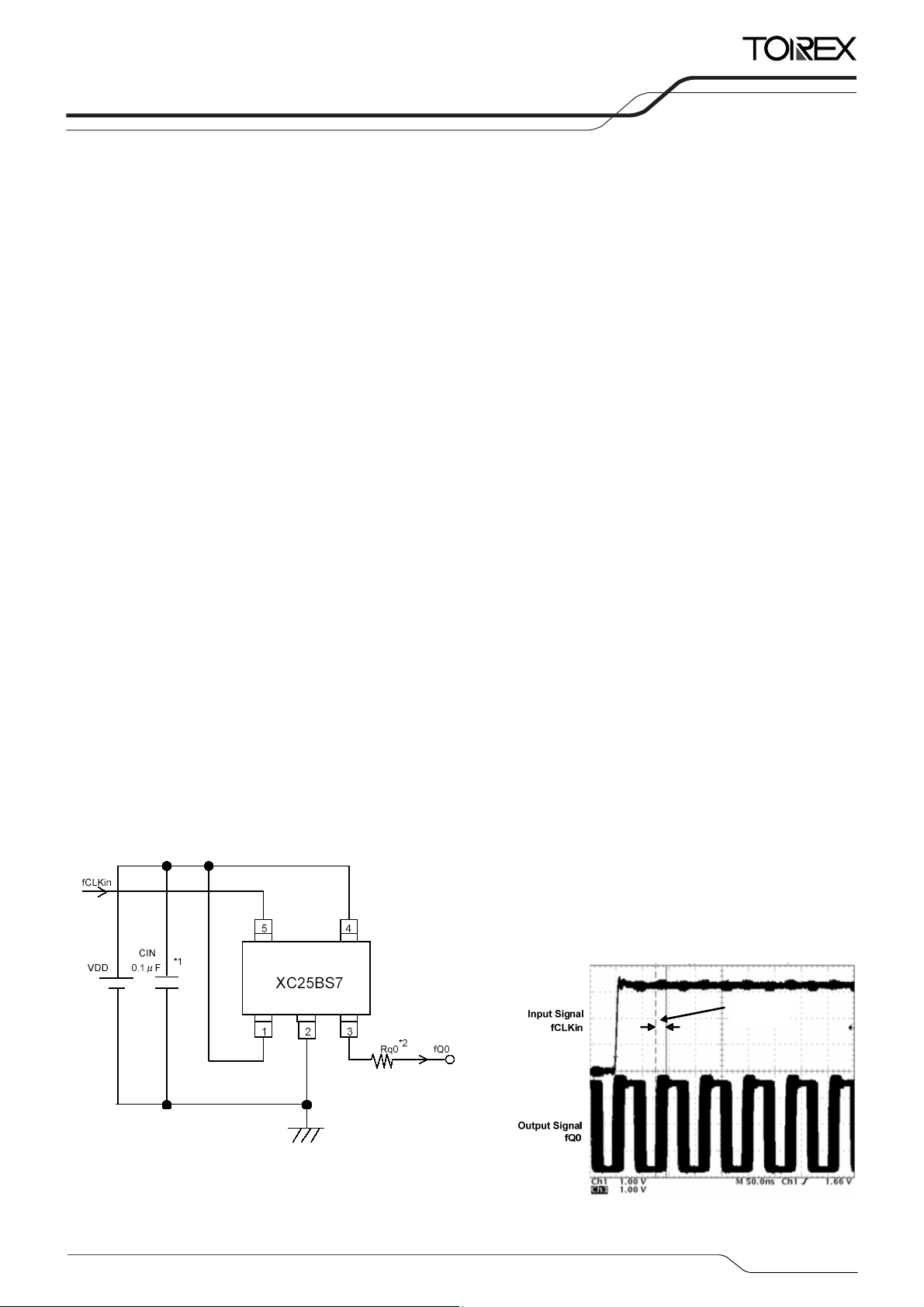
TYPICAL APPLICATION CIRCUIT
*1: C
(by-pass capacitor, 0.1μF) should be connected to the
IN
IC as close as possible.
*2: Rq0 is a resistor for unwanted radiation only to use when
needed.
FEATURES
(*1)
(*1)
(*1)
(*1)
(*1)
Input Frequency : 32kHz ~ 36MHz
Output Frequency : 1MHz ~ 100MHz
(fQ0=fCLKin × N/M)
Output Divider (N) : Selectable from divisions
from 1 to 256
Input Divider (M) : Selectable from divisions
from 1 to 256
Operating Voltage Range : 2.50V ~ 5.50V
Low Power Consumption : CMOS with stand-by function
(10μA, MAX. when stand-by)
Packages
Environmentally Friendly
*1: The series are semi-custom products. Specifications for
each product are limited within the above range. The input
frequency range is set within ±5% of customer’s designated
typical frequency.
*2: When the IC is in stand-by mode, the output becomes high
impedance and the IC stops operation.
: SOT-25, USP-6C
:EU RoHS Compliant, Pb Free
TYPICAL PERFORMANCE
CHARACTERISTICS
● PLL output signal jitter 2 (equivalent to an input signal)
XC25BS7001xx (256 multiplier, Input 48kHz, TYP.)
Output jitter
Tj2=20 (ns)
(*2)
1/13
■
■
■
■
r
XC25BS7 Series
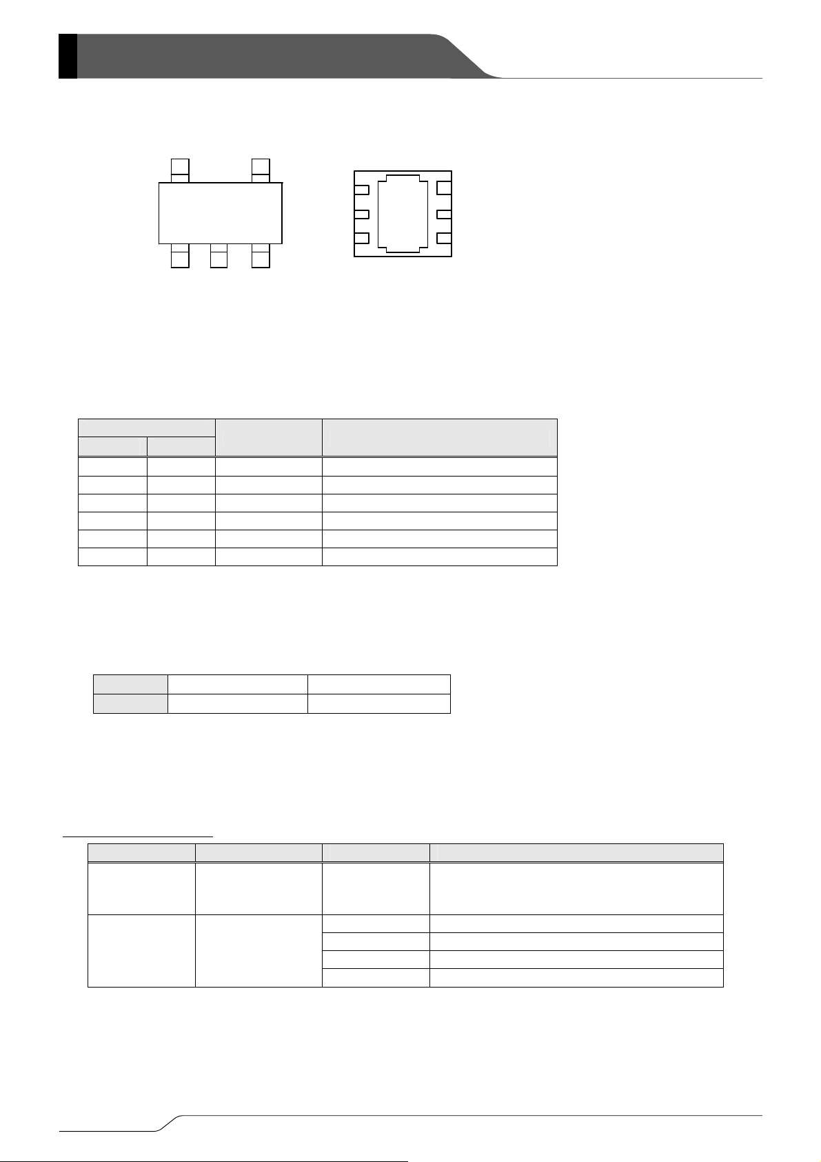
PIN CONFIGURATION
PIN ASSIGNEMNT
CLKin
5 4
1 2 3
CE V
SOT-25
(TOP VIEW)
PIN NUMBER
SOT-25 USP-6C
3 1 Q0 Clock Output
2 2 VSS Ground
1 3 CE Stand-by Control
5 4 CLKin Reference Clock Signal Input
- 5 NC No Connection
4 6 VDD Power Input
FUNCTION LIST
●Ordering Information
XC25BS7①②③④⑤‑⑥
CE 'H'' 'L'' or OPEN
Q0 Signal Output High Impedance
PRODUCT CLASSIFICATION
DESIGNATOR DESCRIPTION SYMBOL DESCRIPTION
Q0
SS
PIN NAME
(*1)
V
DD
DD
V
NC
CLKin
6
5
4
USP-6C
(BOTTOM VIEW)
FUNCTION
Q0
1
V
SS
2
CE
3
* The dissipation pad (TAB) of the
bottom view of the USP-6C package
should be connected to the V
pin.
H: High level input
L: Low level input (stand-by mode)
(No. 2)
SS
2/13
①②③
Product Number Integer
Based on internal standards
e.g. product number 001→①②③=001
MR SOT-25
④⑤-⑥
Packages
Taping Type
(*2)
MR-G SOT-25
ER USP-6C
ER-G USP-6C
(*1)
The “-G” suffix indicates that the products are Halogen and Antimony free as well as being fully RoHS compliant.
(*2)
The device orientation is fixed in its embossed tape pocket. For reverse orientation, please contact your local Torex sales office o
representative. (Standard orientation: ④R-⑥, Reverse orientation: ④L-⑥)
■
■
A
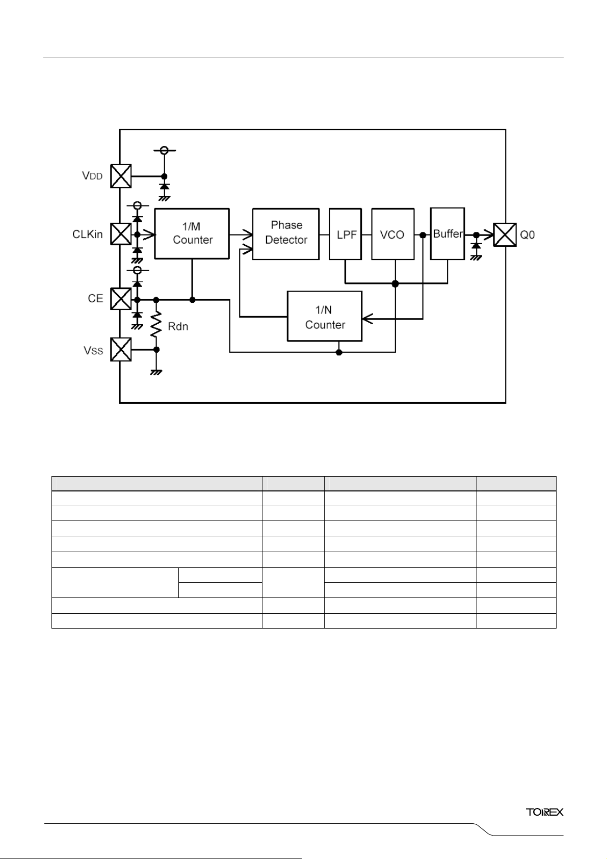
BLOCK DIAGRAM
BSOLUTE MAXIMUM RATINGS
PARAMETER SYMBOL RATINGS UNIT
Supply Voltage VDD
CLKin Pin Input Voltage VCK
CE Pin Input Voltage VCE
Q0 Pin Output Voltage VQ0
Q0 Pin Output Current IQ0 ± 50 mA
Power Dissipation
Operating Temperature Range Topr
Storage Temperature Range Tstg
SOT-25
USP-6C
Pd
- 0.3 ~ VSS + 7.0
V
SS
- 0.3 ~ VDD + 0.3
V
SS
- 0.3 ~ VDD + 0.3
V
SS
- 0.3 ~ VDD + 0.3
V
SS
150
100
-40 ~+85 ℃
-55 ~+125 ℃
XC25BS7
Series
Ta =2 5 ℃
V
V
V
V
mW
mW
3/13
■
XC25BS7 Series
ELECTRICAL CHARACTERISTICS
●Characteristics example by product series
*1: The chart below introduces the products with typical specification characterisitecs which is under production or
production in the past.
*2: The series are semi-custom products. Specifications for each product are limited within the range below.
The input frequency is set within ±5% of customer’s designated typical frequency.
*3: For other part number with other input-output frequency or multiplication, please ask Torex sales contacts.
XC25BS7001xx (256 multiplication)
PARAMETER SYMBOL MIN. TYP. MAX. UNIT
Input Frequency fCLKin - 48.000 - kHz
Multiplier/Divider Ratio N/M - 256 - Multiplier
PLL Output Frequency fQ0 - 12.288 - MHz
XC25BS7007xx (0.333 multiplication)
PARAMETER SYMBOL MIN. TYP. MAX. UNIT
Input Frequency fCLKin - 16.9344 - MHz
Multiplier/Divider Ratio N/M - 0.333 - Multiplier
PLL Output Frequency fQ0 - 5.6448 - MHz
XC25BS7008xx (256 multiplication)
PARAMETER SYMBOL MIN. TYP. MAX. UNIT
Input Frequency fCLKin - 44.000 - kHz
Multiplier/Divider Ratio N/M - 256 - Multiplier
PLL Output Frequency fQ0 - 11.264 - MHz
XC25BS7012xx (256 multiplication)
PARAMETER SYMBOL MIN. TYP. MAX. UNIT
Input Frequency fCLKin - 92.000 - kHz
Multiplier/Divider Ratio N/M - 256 - Multiplier
PLL Output Frequency fQ0 - 23.552 - MHz
XC25BS7013xx (128 multiplication)
PARAMETER SYMBOL MIN. TYP. MAX. UNIT
Input Frequency fCLKin - 184.000 - kHz
Multiplier/Divider Ratio N/M - 128 - Multiplier
PLL Output Frequency fQ0 - 23.552 - MHz
4/13

■
XC25BS7
ELECTRICAL CHARACTERISTICS (Continued)
●Recommended Operating Conditions: XC25BS7001xx (256 multiplication, Input 48kHz (TYP.)) 3.3V (TYP.)
PARAMETER SYMBOL CONDITIONS MIN.
Supply Voltage VDD 3.3V (TYP.) operation
Input Frequency fCLKin
Multiplier/Divider Ratio N/M Typical value is shown
Output Frequency fQ0
Capacity Overload
Output Start Time
NOTE:
*1: Connected C
*2: Time until signal via the Q0 pin flows stably from applying supply voltage to the V
applying the input signal to the CLKin pin.
*3: The value indicated at output start time is designed values which are not guaranteed values.
●DC Characteristics: XC25BS7001xx (256 multiplication, Input 48kHz (TYP.) ) 3.3V (TYP.)
IN
(*3)
CL
(*2)(*3)
t
=0.1μF of a ceramic capacitor between the V
START
Test Conditions: V
(*1)
(*1)
fCLKin=45kHz
pin the V
DD
(*1)
pin while testing.
SS
=3.3V, fCLKin=48kHz, Multiplier ratio=256, Ta=25℃, No Load
DD
PARAMETER SYMBOL CONDITIONS
2.97 3.63
45.000 60.000
11.520 15.360
- 15
0.05 20
pin and control voltage to the CE pin while
DD
MIN. TYP. MAX. UNIT CIRCUIT
H Level Input Voltage VIH 2.70 - - V
L Level Input Voltage VIL - - 0.60 V
H Level Input Current
L Level Input Current
H Level Output Voltage
L Level Output Voltage
Supply Current 1
Supply Current 2
CE H Level Voltage
CE L Level Voltage
CE Pull-Down Resistance 1
CE Pull-Down Resistance 2
Output Off Leak Current
●AC Characteristics: XC25BS7001xx (256 multiplication, Input 48kHz (TYP.)) 3.3V (TYP.)
PARAMETER SYMBOL CONDITIONS
Output Rise Time
Output Fall Time
Output Signal Duty
PLL Output Signal Jitter 1
PLL Output Signal Jitter 2
NOTE:
*1: Values indicated at the AC Characteristics are designing values, which are not guaranteed values.
(*1)
tr (20% ~ 80%) - 2.5 5.0 ns
(*1)
tf (20% ~ 80%) - 2.5 5.0 ns
(*1)
Duty
(*1)
(*1)
IiH V
CLKin=VDD
IiL V
VOH V
VOL V
I
V
DD1
I
V
DD2
V
2.70 - - V
CEH
V
- - 0.45 V
CEL
=2.97V, IOH=-4mA 2.50 - - V
DD
=2.97V, IOL= 4mA - - 0.40 V
DD
=3.63V, CE= 3.63V - 3.0 6.0 mA
DD
=3.63V, CE= 0.0V - - 10
DD
Rdn1 CE=V
Rdn2 CE=0.1 x V
I
V
OZ
=Q0=3.63V, CE= 0.0V - - 10
DD
Test Conditions: V
-0.3V - - 3.0
=0.3V -3.0 - -
CLKin
0.2 1.0 1.8 MΩ
DD
10 30 60 kΩ
DD
=3.3V, fCLKin=48kHz, Multiplier ratio=256, Ta=25℃, CL=15pF
DD
MIN. TYP. MAX. UNIT CIRCUIT
fQ0≦60MHz
fQ0≧60MHz
45 50 55
40 50 60
tJ1 1σ (Output Period) - 20 - ps
t
J
2
Peak to Peak (Output Tracking) - 20 - ns
256
Tested below Ta=25OC
MAX.
μA ②
μA ②
μA ④
μA ⑥
%
%
Series
UNIT
V
kHz
-
MHz
pF
ms
①
①
③
③
④
①
①
⑤
⑤
①
①
①
①
①
5/13

■
XC25BS7 Series
NOTE ON USE
(1) Please use this IC within the stated absolute maximum ratings. The IC is liable to malfunction should the ratings be
exceeded.
(2) The series is an analog IC. Please use a 0.01μF to 0.1μF of a by-pass capacitor.
(3) Rq0 shown in the Typical Application Circuit is a matching resistor. The use is recommended in order to counter
unwanted radiations.
(4) Please place the by-pass capacitor and the matching resistor as close to the IC as possible. The IC may not operate
normally if the by-pass capacitor is not close enough to the IC. Further, the unwanted radiation may occur between
the resistor and the IC pin if the matching resistor is not close enough to the IC.
(5) When the CE pin is not controlled by external signals, it is recommended that a time constant circuit of R1=1kΩ ×C1
= 0.1μF be added for stability.
(6) With this IC, output is achieved by dividing and multiplying the reference oscillation by means of the PLL circuit. In
cases where this output is further used as a reference oscillation of another PLL circuit, it may be that the final output
signal's jitter increases; therefore, all necessary precautions should be taken to avoid this.
(7) It is recommended that a low noise power supply, such as a series regulator, be used as the series’ supply voltage.
Using a power supply such as a switching regulator may enlarge the jitter, which in turn may lead to abnormal
operation. Please confirm its operation with the actual device.
(8) For operating the IC normally, please take procedures below when applying voltage to the series’ input pin:
1) Apply power source while the CE pin is "L" level with no clock input (high-Impedance or “L”),
2) Input the clock,
3) At least 100μs after applying clock input, change the CE pin into “H” level.
The IC has to be started by inputting the clock once the power rises completely. The CE pin, then, should be enabling.
If the CE pin becomes enable and the clock is inputted before the power rises completely, an internal reset circuit
does not operate normally which may cause to generate extraneous frequency.
(9) As for this IC, synchronization of input and output signals occurs at the rising edge.
6/13

■
TEST CIRCUIT
①Operating Supply Voltage
H Level Input Voltage
L Level Input Voltage
CE “H” Level Voltage
CE “L” Level Voltage
Output Rise Time
Output Fall Time
Output Signal Duty
PLL Output Signal Jitter
②H Level Input Current
L Level Input Current
③H Level Output Voltage
L Level Output Voltage
XC25BS7
Series
7/13

■
XC25BS7 Series
TEST CIRCUIT (Continued)
④Supply Current 1
Supply Current 2
⑤CE Pull-Down Resistance 1
CE Pull-Down Resistance 2
⑥Output Off Leak Current
8/13

■
A
C CHARACTERISTICS TEST WAVEFORM
1) Output Rise Time, Output Fall Time
2) Duty Ratio
3) Output Start Time
t
START
XC25BS7
Series
9/13

■
XC25BS7 Series
TYPICAL PERFORMANCE CHARACTERISTICS
●Output Frequency Range (Capable of Synchronous) vs. Supply Voltage
XC25BS7001xx (256 multiplication, Input 48kHz (TYP.))
10/13

■
PACKAGE INFORMATION
●SOT-25
●USP-6C Reference Mount Pattern ●USP-6C Reference Metal Masking
●USP-6C
* No. 1 pin is larger than the other pins.
Soldering fillet surface is not formed because the
sides of the pins are not plated.
XC25BS7
Series
11/13

⁝⁝⁝
■
XC25BS7 Series
MARKING RULE
●SOT-25
1
2
3
12/13
SOT-25
(TOP VIEW)
●USP-6C
⑤ ⑥④
USP-6C
(TOP VIEW)
①, ② and ③ represents product series
6
② ③①
5
4
① and ② represent product series.
MARK
① ②
B
7
7
S XC25BS7S**M*
PRODUCT SERIES
XC25BS70**M*
③ represents the serial number corresponding to the part number 『b』,『c』.
* The serial numbers after the 99 are repeated as shown below for ④ and ⑤.
MARK
③
『b』 『c』
PART NUMBER
MARK
③
『b』 『c』
PART NUMBER
1 0 1 XC25BS7*01M* K 1 7 XC25BS7*17M*
2 0 2 XC25BS7*02M* L 1 8 XC25BS7*18M*
3 0 3 XC25BS7*03M* M 1 9 XC25BS7*19M*
4 0 4 XC25BS7*04M* N 2 0 XC25BS7*20M*
5 0 5 XC25BS7*05M* P 2 1 XC25BS7*21M*
6 0 6 XC25BS7*06M* R 2 2 XC25BS7*22M*
7 0 7 XC25BS7*07M* S 2 3 XC25BS7*23M*
8 0 8 XC25BS7*08M* T 2 4 XC25BS7*24M*
9 0 9 XC25BS7*09M* U 2 5 XC25BS7*25M*
A 1 0 XC25BS7*10M* V 2 6 XC25BS7*26M*
B 1 1 XC25BS7*11M* X 2 7 XC25BS7*27M*
C 1 2 XC25BS7*12M* Y 2 8 XC25BS7*28M*
D 1 3 XC25BS7*13M* Z 2 9 XC25BS7*29M*
E 1 4 XC25BS7*14M* 1 3 0 XC25BS7*30M*
F 1 5 XC25BS7*15M* 2 3 1 XC25BS7*31M*
H
6 XC25BS7*16M*
1
⁝
⁝
④ and ⑤ represents production lot number
01,…09,10,11,…,99, 0A,…,0Z,1A,…,9Z,A0,…,Z9,AA,…ZZ are used in series.
(G, I, J, O, Q, and W are excluded from the serial numbers.)
* Inverted characters are not used.
MARK
① ② ③
B S
S
7
7
S XC25BS7S**E*
PRODUCT SERIES
XC25BS70**E*
④ and ⑤ represents product serial numbers (④= 『b』, ⑤= 『c』)
MARK
④ ⑤
MARK
PART NUMBER
『b』 『c』
0 1 XC25BS7001E*
0 2 XC25BS7S02E*
⑥ represents production lot number
0〜9, A〜Z repeated (G, I, J, O, Q, and W are excluded from the serial numbers)
* Inverted characters are not used.
⁝

XC25BS7
Series
1. The products and product specifications contained herein are subject to change without
notice to improve performance characteristics. Consult us, or our representatives
before use, to confirm that the information in this datasheet is up to date.
2. We assume no responsibility for any infringement of patents, patent rights, or other
rights arising from the use of any information and circuitry in this datasheet.
3. Please ensure suitable shipping controls (including fail-safe designs and aging
protection) are in force for equipment employing products listed in this datasheet.
4. The products in this datasheet are not developed, designed, or approved for use with
such equipment whose failure of malfunction can be reasonably expected to directly
endanger the life of, or cause significant injury to, the user.
(e.g. Atomic energy; aerospace; transport; combustion and associated safety
equipment thereof.)
5. Please use the products listed in this datasheet within the specified ranges.
Should you wish to use the products under conditions exceeding the specifications,
please consult us or our representatives.
6. We assume no responsibility for damage or loss due to abnormal use.
7. All rights reserved. No part of this datasheet may be copied or reproduced without the
prior permission of TOREX SEMICONDUCTOR LTD.
13/13
 Loading...