

XC25BS6 Series
y
X
(
)
y
查询XC25BS6供应商
Divider Signal Output Clock Generator ICs with Built-In Crystal Oscillator Circuit September 17, 2003 V1
Preliminary
CMOS Low Power Consumption APPLICATIONS
Low Operating Supply Voltage 2.3V (MIN.) z
Output Frequency 32.768kHz z Clocks for Micro-computers, DSPs, etc.
Oscillation Frequency 2MHz ~ 36MHz (fundamental) z Communication Equipment
Built-In Divider Circuit Selectable from divisions of z Various System Clocks
1024, 512, 256, 128 z Clock Time-Base
Output 3-State
Ultra Small Package SOT-26
Chip Form
GENERAL DESCRIPTION FEATURES
The XC25BS6 is a low operating voltage, low current consumption
series of CMOS ICs with built-in crystal oscillator and divider circuits
designed for clock generators. Oscillation capacitors Cg and Cd are
externally set up.
Output is selectable from any one of the following values for f0:f0/1024,
f0/512, f0/256, and f0/128.
With oscillation feedback resistors built-in, it is possible to configure a
stable fundamental oscillator using about 10pF of external oscillation
capacitor and an external crystal.
The series has a stand-by function. The oscillation completely stops in
the stand-by state and output will be one of high-impedance.
Crystal Oscillation Modules
Oscillation Frequency 2MHz ~ 36MHz (fundamental)
- Oscillation feedback resistor built-in
- External oscillation capacitor
Divider Ratio f0/1024, f0/ 512, f0/256, f0/128
Output 3-State
Operating Supply 2.3 ~ 4.0V
Voltage Range
Supply Current 0.5µA (MAX.) when stand-by mode
Chip Form Chip size 1.3 x 0.8mm
Package SOT-26 mini mold
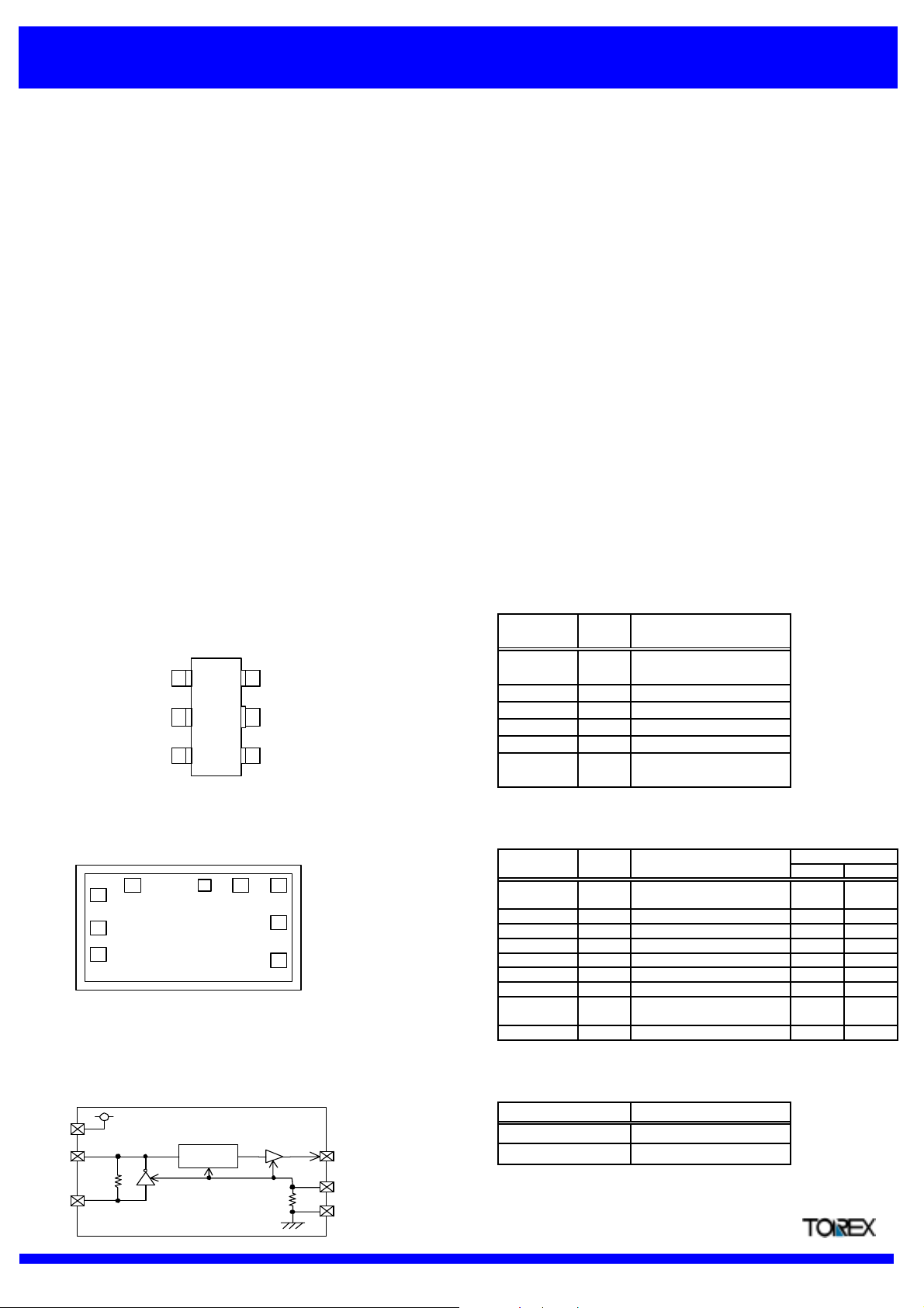
PIN CONFIGURATION PIN ASSIGNMENT
PIN
NAME
FUNCTIONS
Crystal Oscillator
Connection (Output)
VSS Ground
Q0
CE
Clock Output
Stand-by Control *
Power Supply
Crystal Oscillator
Connection (Input)
VSS
Q0
PIN NUMBER
1/XT
XT
6
1 / XT
2
VDD
2
3
5
4
CE
3
4
5 VDD
6XT
* The stand-by control pin (pin #4) has a pull-down resistor built-in.
PAD LAYOUT FOR CHIP FORM PAD LOCATIONS (Unit:µm)
(0,0)
VSS
/XT
VDD
XT
Chip Size
Chip Thickness
Chip Back
Pad Aperture
(NC)
VSS
: 1300 x 800µm
: 280±20µm
: VDD level
: 88 x 88 µm
Q0
VDD
CE
(1300,800)
Note)
There are two VSS
pads and two VDD
pads. Please connect
both VSS pads to
GND, and connect
both VDD pads to a
power supply.
PIN NUMBER
1
2
PIN
NAME
/ XT
VSS
FUNCTIONS
Crystal Oscillator
Connection
Output
Ground
3 (NC) No Connection 741.0
4 VSS Ground 952.0
5
6
Q0
VDD
7
8
XT 128.0
Clock Output
Power Suppl
Stand-by Control *
Crystal Oscillator
Connection (Input)
9 VDD Power Suppl
* The stand-by control pin (pin #4) has a pull-down resistor built-in.
PAD DIMENSIONS
Y
128.0 610.0
328.0 672.0
672.0
672.0
1172.0
672.0
1172.0 430.0
1172.0CE
189.0
187.0
128.0
399.0
BLOCK DIAGRAM CE, Q0 PIN FUNCTION
VDD
/XT
Counter
XT
Q0
CE
VSS
Data Sheet 1
CE
'H'
'L' or Open High Impedance
Q0
Clock Output
Semi conductor Ltd.
XC25BS6 Series
K
K
Divider Signal Output Clock Generator ICs with Built-In Crystal Oscillator Circuit
Preliminary
ABSOLUTE MAXIMUM RATINGS
Ta=25OC
SYMBOL RATINGS UNITSPARAMETER
VDD VSS -0.3 ~ VSS +7.0 VSupply Voltage
CE Pin Voltage
Q0 Pin Voltage
Operating Temperature Range
** SOT-26 package, When implemented on a glass epoxy PCB.
PRODUCT CLASSIFICATION
Ordering Information
XC25BS6
12345
123
Divider Ratio: Package:
128 = 128 divider C : Chip Form
256 = 256 divider W : Wafer Form
512 = 512 divider M : SOT-26
A24 = 1024 divider Device Orientation:
VCE VSS -0.3 ~ VDD +0.3
VQ0 VSS -0.3 ~ VDD +0.3
IQ0
Pd 150 ** mWContinuous Power Dissipation
Topr - 40 ~ + 85
- 65 ~ + 150 (Chip Form)
- 55 ~ + 125 (SOT-26)
DESCRIPTIONDESIGNATOR DESIGNATOR
± 50
4
5
V
V
mAQ0 Output Current
O
C
O
CTstgStorage Temperature Range
DESCRIPTION
R : Embossed Tape : Standard Feed
L : Embossed Tape : Reverse Feed
T : Chip Tray
W : Wafer
MARKING RULE
654
1 2 3 4
3
21
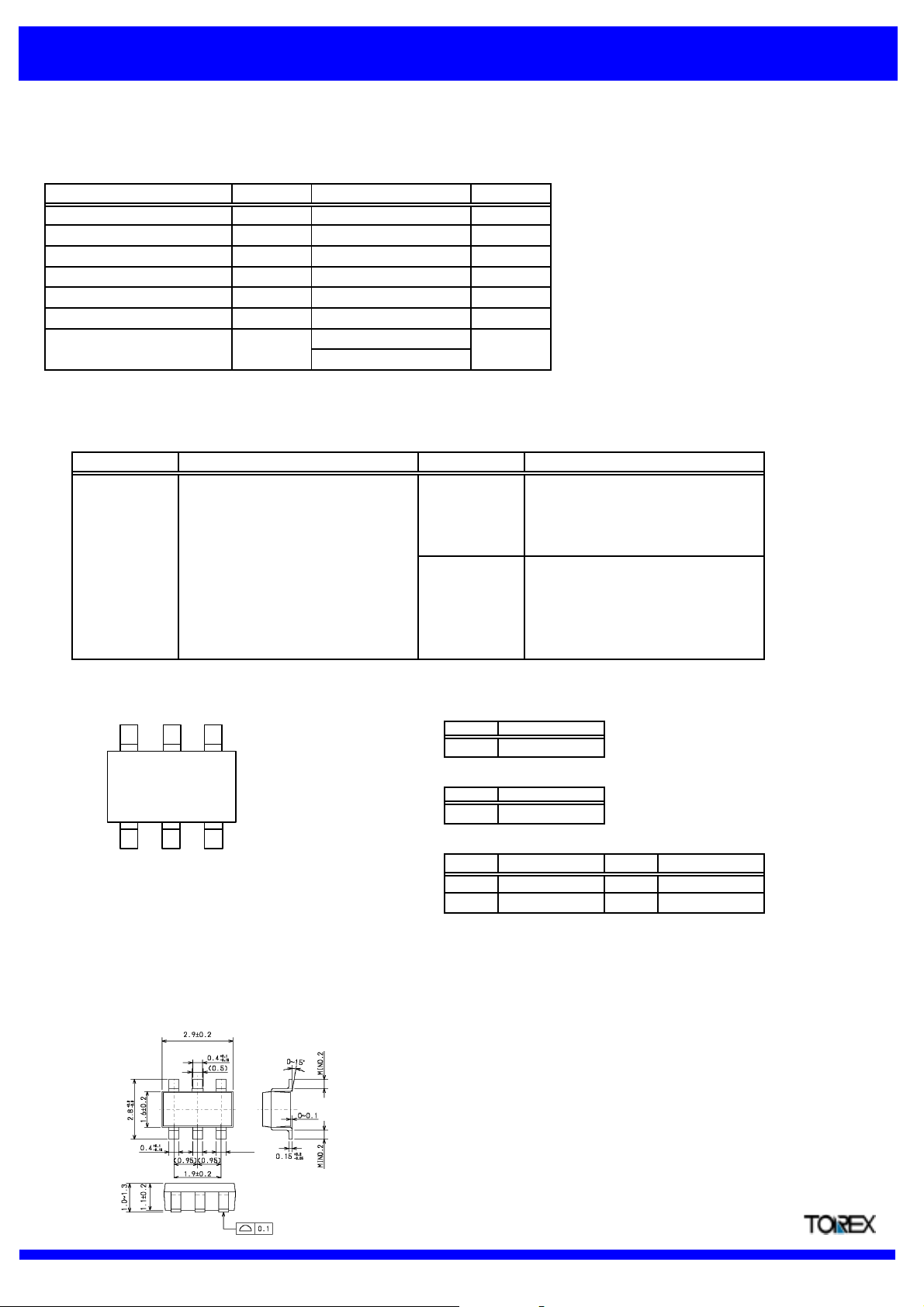
PACKAGING INFORMATION
SOT-26
1 Represents XC25BS6 Series
MAR
Product Name
B XC25BS6
2 Represents XC25BS6 Series
MAR
Product Name
6 XC25BS6
3 Represents divider ratio
MARK
1
5
Divider Ratio
f0/128
f0/512
4 Represents the assembly lot no.
(Based on internal standards)
MARK Divider Ratio
2 f0/256
A f0/1024
Semi conductor Ltd.
Data Sheet 2

XC25BS6 Series
Divider Signal Output Clock Generator ICs with Built-In Crystal Oscillator Circuit
Preliminary
WIRE BONDING CONNECTION
VSS
/XT
VDD
XT
* There are two VSS pads and VDD pads.
Please connect both VSS pads to GND, and connect both VDD pads to a power supply.
TYPICAL APPLICATION CIRCUIT
CgCd
* Please use oscillation capacitors Cg, Cd =10pF externally
* The same power supply can be used for VDD and CE.
(NC)
VSS
VDD
/XT
XT VSS
0.1uF
Q0
VDD
CE
Q0
CE
Rq0
fQ0 measurement
NOTES ON USE
(1) The oscillation circuit of this IC does not have internal oscillation capacitors.
Please make the oscillation circuitry using an external crystal transducer and oscillation capacitors Cg and Cd.
*) A higher harmonic wave oscillation may occur without Cg and Cd.
*) Cg and Cd can be connected either to GND or VDD. (Cg and Cd in the above circuit example are connected to GND.)
*) It is recommended to use around for 10pF of Cg and Cd. For trimmer capacitors, 10pF as a standard value is appropriate.
*) The crystal oscillation frequency should be measured at the output of the Q0 pin.
When a probe is directly connected to the XT pin or the /XT pin, oscillation frequency will change and a precise value can not be taken.
(2) Please insert a by-pass capacitor of 0.1µF between VDD and GND.
(3) The use of a matching resistor Rq0 of 50Ω connected in series to the Q0 pin is recommended in order to counter unwanted radiations.
(4) Please place a by-pass capacitor and the matching resistor as close to the IC as possible. If the by-pass capacitor is placed away from the IC, it
may cause abnormal oscillation. If the matching resistor is placed away from the IC, it may cause unwanted radiations in the pattern between the
Q0 pin and the resistor.
(5) When the CE pin is not controlled by external signals, please connect the CE pin to VDD power supply.
*) When the CE pin is not connected, the IC goes into stand-by mode due to the internal pull-down resistor.
(6) As for the supply voltage, it is recommended to apply a low noise power supply, such as a series regulator. Using a power supply like a switching
regulator might lead to an unstable oscillation jitter which in turn may lead the oscillation frequency to fluctuate due to the ripple of the switching
regulator.
Data Sheet 3
Semi conductor Ltd.

XC25BS6 Series
Divider Signal Output Clock Generator ICs with Built-In Crystal Oscillator Circuit
Preliminary
DC ELECTRICAL CHARACTERISTICS
XC25BS6xxxxx 3.0V Operation (unless otherwise stated, VDD=3.0V, fOSC=16MHz, No load, Ta=25OC)
PARAMETER
Operating Supply Voltage
Crystal Oscillation Frequency
H Level Output Voltage
L Level Output Voltage
Supply Current 1
Supply Current 2
CE H Level Voltage
CE L Level Voltage
CE Pull-Down Resistance 1
CE Pull-Down Resistance 2
Internal Oscillation Feedback Resistance
Output Disable Leakage Current
SYMBOL
VDD
fOSC
VOH
VOL
IDD1
IDD2
VCEH
VCEL
Rp1
Rp2
Rf
IOZ
FUNCTIONS
Cf=Cd=10pF (External)
VDD=2.7V, IOH= - 4mA
VDD=2.7V, IOL=4mA
fOSC=4MHz, XC25BS6128
CE=3.0V
fOSC=8MHz, XC25BS6256
fOSC=16MHz, XC25BS6512
fOSC=36MHz, XC25BS6A24
CE=3.0V
CE=0.3V
XT Pin, CE=/XT=3.0V
Q0 Pin, VDD=4.0V, CE=0V
CE=0V
STANDARD VALUE
MIN TYP MAX
(2.3) 3.0 4.0
2-36
2.3 - -
- - 0.4
- (0.4) (0.8)
- (0.5) (1.0)
- (0.8) (1.6)
- (1.0) (1.8)
-
2.4
0.5 1.6
22
0.2 0.5 1.0
-
- 0.5
--
- 0.6
3.0
55 90
- 0.5
* External oscillation capacitor
UNIT
V
MHz
V
V
mA
µA
V
V
MΩ
KΩ
MΩ
µA
AC ELECTRICAL CHARACTERISTICS
XC25BS6xxxxx 3.0V Operation (unless otherwise stated, VDD=3.0V, fOSC=16MHz, CL=15pF, Ta=25OC)
PARAMETER
Output Rise Time Tr VDD=3.0V (10% to 90%) *1 -
Output Fall Time Tf VDD=3.0V (10% to 90%) *1
Duty Cycle DUTY 45
Output Start Time Ton *1 -
SYMBOL
FUNCTIONS
STANDARD VALUE
MIN TYP MAX
10 15 ns
-
10 15 ns
50 55
-
3.0
*1 R&D guarantee
AC ELECTRICAL CHARACTERISTICS MEASUREMENT WAVE FORMS
(1) Output Rise Time , Output Fall Time
0.9VDD
0.1VDD
tr tf
(2) Duty Cycle
0.9VDD
0.1VDD
UNIT
%
ms
DUTY Measurement Level
TW
T DUTY = (TW/T) x 100 [%]
Data Sheet 4
0.5VDD
Semi conductor Ltd.
 Loading...