


■
■
■
■
■
XC25BS5 Series
ETR1502_003a
PLL Clock Generator ICs with Built-In Divider/Multiplier Circuits
(For Low Frequency Range)
GENERAL DESCRIPTIO N
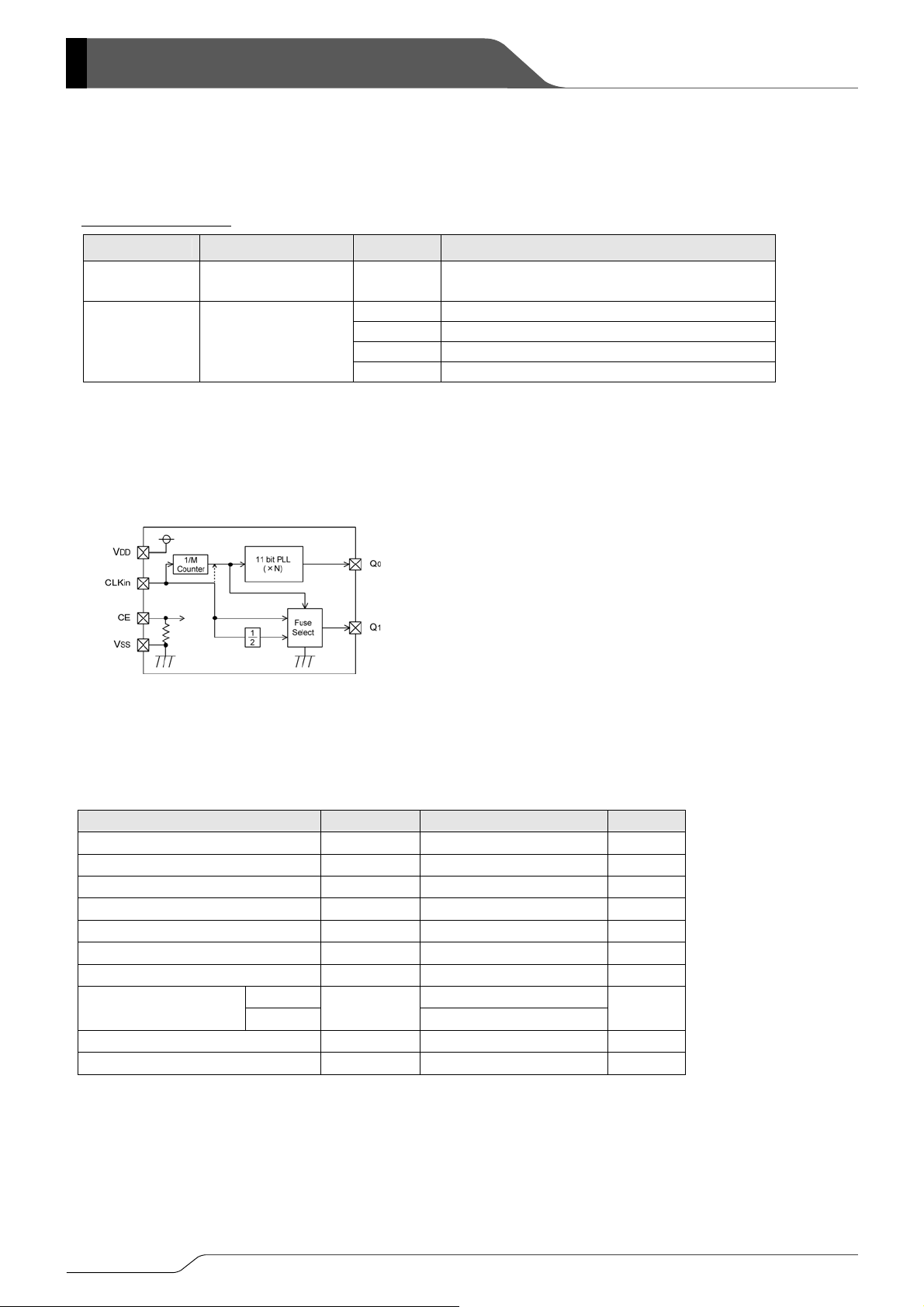
The XC25BS5 series are high frequency, low power consumption PLL clock generator ICs with divider circuit & multiplier
PLL circuit.
Laser trimming gives the option of being able to select from divider ratios (M) of 1,3 to 2047 and multiplier ratios (N) of 6 to
2047.
Output frequency (Q0) is equal to reference oscillation (fCLKin) multiplied by N/M, within a range of 3MHz to 30MHz. Q1
output is selectable from input reference frequency (f0), input reference freque ncy/2 (f0/2) , ground (GND), and comparative
frequency (f0/M). Further, comparative frequencies, within a range of 12KHz to 500KHz, can be obtained by dividing the
reference oscillation. By halting operation via the CE pin, consumption current can be controlled and output will be o ne of
high-impedance.
■APPLICATIONS
●Crystal oscillation modules
●Personal computers
●PDAs
●Portable audio systems
●Various system clocks
PIN CONFIGURATION
SOT-26
(TOP VIEW)
*The dissipation pad for the USP-6B package
should be solder-plated in recommended mount
pattern and metal masking so as to enhance
mounting strength and heat release.
If the pad needs to be connected to other pins,
it should be connected to the V
FUNCTION LIST
C E FUNCTION
●CE, Q0/Q1 Pin Function
"H" Q0, Q1 Clock Output
"L" Stand-by. Output Pin = High Impedance
Open
Stand-by. Output Pin = High Impedance
(V
SS Pin Pull-Down Due to IC's Internal Resistor)
Q1 6
VDD 5
CLKin 4
USP-6B
(BOTTOM VIEW)
1 Q0
2 VSS
3 CE
DD pin.
FEATURES
Output Frequency : 3MHz ~ 30MHz (Q0=fCLKin×N/M)
Input Frequency (fCLKin)
: 12kHz ~ 35MHz
Divider Ratio (M) :
Multiplier Ratio (N) :
Output : 3-State
Operating Voltage Range
: 2.97V ~ 5.5V
Low Power Consumption
: CMOS (stand-by function included)*1
Comparative Frequency
: 12kHz~500kHz
Package
Environmentally Friendly
Selectable from divisions of 1, 3~2047
Selectable from multiplications of 6~2047
Q1
output selectable from input reference
oscillation, input reference oscillation/2,
GND, comparative frequency.
: SOT-26, USP-6B
*1 High output impedance during standby
: EU RoHS Compliant, Pb Free
PIN ASSIGNMENT
PIN NUMBER
SOT-26 USP-6B
1 3 CE Chip Enable
2 2 VSS GND
3 1 Q0 PLL Output
4 6 Q1
5 5 VDD Power Supply
6 4 CLKin Reference Clock Input
"H" = High level
"L" = Low level
PIN
NAME
FUNCTION
Reference Oscillation,
Reference Oscillation/2,
GND, or Comparative
Frequency Output
1/12
■
■
■
A
XC25BS5 Series
PRODUCT CLASSIFICATION
●Ordering Information
XC25BS5①②③④⑤-⑥
DESIGNATOR DESCRIPTION SYMBOL DESCRIPTION
①②③
④⑤-⑥
(*1)
The “-G” suffix indicates that the products are Halogen and Antimony free as well as being fully RoHS compliant.
(*2)
The device orientation is fixed in its embossed tape pocket. For reverse orientation, please contact your local Torex
sales office or representative. (Standard orientation: ④R-⑥, Reverse orientation: ④L-⑥)
ٛ
BLOCK DIAGRAM
BSOLUTE MAXIMUM RATINGS
PARAMETER SYMBOL CONDITIONS UNITS
Supply Voltage VDD VSS-0.3 ~ VSS+7.0 V
CLKin Pin Voltage VCK VSS-0.3 ~ VDD+0.3 V
CE Pin Voltage VCE VSS-0.3 ~ VDD+0.3 V
Q0 Pin Voltage VQ0 VSS-0.3 ~ VDD+0.3 V
Q1 Pin Voltage VQ1 VSS-0.3 ~ VDD+0.3 V
Q0 Output Current IQ0 ±50 mA
Q0 Output Current IQ1 ±50 mA
Power Dissipation
Operating Temperature Range Topr - 30 ~ + 80 ℃
Storage Temperature Range Tstg - 40 ~ +125 ℃
(*1)
Product Number Integer
MR SOT-26
Packages
Taping Type
SOT-26 150
USP-6B
(*2)
MR-G SOT-26
DR USP-6B
DR-G USP-6B
Pd
Based on internal standards
e.g. Product number 001 → ①②③ = 001
Ta = 25℃
100
mW
2/12
■
FREQUENCY CONFIGURATION: EXAMPLE 1
XC25BS51XXMR
● Electrical Characteristics (DC)
XC25BS51xxMR
PARAMETER SYMBOL MIN. TYP. MAX. UNITS
Input Frequency f CLKin 11.0000 - 16.9344 MHz
Multiplier/Divider Ratio N/M - 1.594 - PLL Output Frequency fQ0 17.5383 - 27.0000 MHz
Q1 Output Frequency Q1 GND -
fCLKin = 16.9344MHz, Multiplier/Divider Ratio = 1.594, Ta = 25℃, No Load
PARAMETER SYMBOL CONDITIONS MIN. TYP. MAX. UNITS
Supply Voltage VDD 2.97 3.30 3.63 V
Input Voltage "High" VIH 2.7 - - V
Input Voltage "Low" VIL - - 0.6 V
Input Current "High" IIH VCK = 3.3V - - 3.0
Input Current "Low" IIL VCK = 0V -3.0 - -
Output Voltage "High" VOH VDD = 2.97V, IOH = -8mA 2.5 - - V
Output Voltage "Low" VOL VDD = 2.97V, IOL = 8mA - - 0.4 V
Supply Current 1 IDD1 CE = 3.3V - 3.0 6.0 mA
Supply Current 2 IDD2 CE = 0V - - 5.0
XC25BS5
Series
μA
μA
μA
CE "High" Voltage VCEH 2.7 - - V
CE "Low" Voltage VCEL - - 0.45 V
CE Pull-Down Resistance 1 Rp1 CE = 3.3V 0.5 1.5 2.5
CE Pull-Down Resistance 2 Rp2 CE = 0.3V 20.0 50.0 80.0
● Electrical Characteristics (AC)
XC25BS51xxMR
fCLKin=16.9344MHz, Multiplier/Divider Ratio=1.594, Ta=25℃, CL=15pF
PARAMETER SYMBOL CONDITIONS MIN. TYP. MAX. UNITS
Output Rise Time TTLH VDD=3.3V(20% to 80%) (*1) - 5.0 - ns
Output Fall Time TTHL VDD=3.3V(20% to 80%) (*1) - 5.0 - ns
Duty Ratio DUTY 40 50 60 %
Output Start Time Ton (*1) - - 20 ms
PLL Output Jitter Tj
1σ (*1)
- 40 - ps
MΩ
kΩ
*1 R&D guarantee
3/12
■
XC25BS5 Series
FREQUENCY CONFIGURATION: EXAMPLE 2
XC25BS51XXMX
●Electrical Characteristics (DC)
XC25BS51xxMR
CE Pull-Down Resistance 1 Rp1 CE=3.3V 0.5 1.5 2.5
CE Pull-Down Resistance 2 Rp2 CE=0.3V 20.0 50.0 80.0
● Electrical Characteristics (AC)
XC25BS51xxMR
PARAMETER SYMBOL MIN. TYP. MAX. UNITS
Input Frequency f CLKin 52.0000 - 78.0000 kHz
Multiplier/Divider Ratio N/M - 256.000 - PLL Output Frequency fQ0 13.312 - 19.968 MHz
Q1 Output Frequency Q1 GND -
PARAMETER SYMBOL CONDITIONS MIN. TYP. MAX. UNITS
Supply Voltage VDD 2.97 3.30 3.63 V
Input Voltage "High" VIH 2.7 - - V
Input Voltage "Low" VIL - - 0.6 V
Input Current "High" IIH VCK=3.3V - - 3.0
Input Current "Low" IIL VCK=0V -3.0 - -
Output Voltage "High" VOH VDD=2.97V, IOH= - 8mA 2.5 - - V
Output Voltage "Low" VOL VDD=2.97V, IOL=8mA - - 0.4 V
Supply Current 1 IDD1 CE=0.3V - 2.0 4.0 mA
Supply Current 2 IDD2 CE=0V - - 5.0
CE " High " Voltage VCEH 2.7 - - V
CE "Low" Voltage VCEL - - 0.45 V
PARAMETER SYMBOL CONDITIONS MIN. TYP. MAX. UNITS
Output Rise Time TTLH VDD=3.3V(20% to 80%) (*1) - 5.0 - ns
Output Fall Time TTHL VDD=3.3V(20% to 80%) (*1) - 5.0 - ns
Duty Ratio DUTY 40 50 60 %
Output Start Time Ton (*1) - - 20 ms
PLL Output Jitter Tj
1σ (*1)
fCLKin=78kHz, Multiplier/Divider Ratio=256, Ta=25℃, No Load
μA
μA
μA
MΩ
KΩ
fCLKin=78kHz, Multiplier/Divider Ratio=256, Ta=25℃, CL=15pF
- 20 - ps
*1 R&D guarantee
4/12

■
■
XC25BS5
TYPICAL APPLICATION CIRCUITS
① Q1 Pin - reference oscillation, reference oscillation/2, comparative frequency
② Q1 Pin - GND
NOTE
(1) Please insert a by-pass capacitor of 0.1μF.
(2) Rq0 and Rq1 are matching resistors. Their use is recommended in order to counter unwanted radiations.
(3) Please place a by-pass capacitor and matching resistors as close to the IC as possible. It may be that the
output cannot be locked if the by-pass capacitor is not close enough to the IC. Further, there is a possibility of
unwanted radiation occurrence between the resistor and the IC pin if the matching resistor is not close enough to
the IC.
(4) When selecting GND for the Q1 pin, although the output of Q1 pin is GND level, it is also recommended that the
Q1 pin be connected to GND pattern on the PCB.
(5) When the CE pin is not controlled by external signals, it is recommended that a time constant circuit of R1=1kΩ
×C1 = 0.1μF be added for stability.
(6) With this IC, output is achieved by dividing and multiplying the reference oscillation by means of the PLL circuit.
In cases where this output is further used as a reference oscillation of another PLL circuit, it may be that the final
output signal's jitter increases, so all necessary precautions should be taken to avoid this.
(7) It is recommended that a low noise power supply, such as a series regulator, be used for the supply voltage.
Using a power supply such as a switching regulator might lead to a larger jitter, which in turn may lead to an
inability to lock due to the ripple of the switching regulator.
(8) As for this IC, synchronization of input and output signal’s edge is not guaranteed though the input frequency
operates to the output frequency multiply.
Series
5/12

■
XC25BS5 Series
REFERENCE LAND PATTERN
① Q1 Pin - reference oscillation, reference oscillation/2, comparative frequency
② Q1 Pin - GND
6/12

■
A
C CHARACTERISTIC WAVEFORMS
1) Output Rise Time / Output Fall Time
2) Duty Ratio
3) Output Start Time
XC25BS5
Series
DUTY Measurement Level
DUTY Measurement Level
7/12

■
XC25BS5 Series
PACKAGING INFORMATION
●SOT-26
+0.1
0.4
-0.05
2.9±0.2
(0.5)
5
6 4
1
2
(0.95)
(0.95)
3
0.15
+0.1
-0.05
0~0.1
●USP-6B Reference Pattern Layout
2.4
0.45
0.45
●USP-6B
2.0±0.05
(0.125)
0.65±0.05
0.7±0.03
0.65±0.05
1.0±0.05
0.25±0.05 0.25±0.05
●USP-6B Reference Metal Mask Design
2.3
0.35
0.35
8/12
1
2
3
6
5
2
61
5
4
34
0.05
1.0
0.05
0.15
0.15
0.8

■
2
)
MARKING RULE
●SOT-26
SOT-26
(TOP VIEW)
●USP-6B
1
⑤ ⑥④
3
USP-6B
(TOP VIEW)
② ③①
●XC25BS50 ●XC25BS51
①② represents product series ① represents product series
MARK
① ②
PRODUCT SERIES
MARK PRODUCT SERIES
5 XC25BS51**M*
B 5 XC25BS50**M*
③ represents the 10th digit of product
part number
MARK PRODUCT SERIES
1 XC25BS5001M*
5 XC25BS5005M*
②③ represents the 9th and 10th digits of
product part number
MARK
② ③
0 7 XC25BS5107M*
6 XC25BS5006M*
④ represents production lot number
0 to 9,A to Z reversed character 0 to 9,A to Z repeated (G, I, J, O, Q, W excluded)
①,②,③ represents product series
MARK
6
5
4
① ② ③
B S 0 XC25BS50**D*
B S 1 XC25BS51**D*
PRODUCT SERIES
④⑤ represents the 9th and 10th digit of product part number
Ex
MARK
④ ⑤
PRODUCT SERIES
0 7 XC25BS5*07D*
⑥ represents production lot number
0 to 9,A to Z repeated (G, I, J, O, Q, W excluded)
Note: No character inversion used.
XC25BS5
Series
PRODUCT SERIES
9/12

XC25BS5 Series
■PACKAGING INFORMATION (Continued)
● SOT-26 Power Dissipation
Power dissipation data for the SOT-26 is shown in this page.
The value of power dissipation varies with the mount board conditions.
Please use this data as one of reference data taken in the described condition.
1. Measurement Condition (Reference data)
Copper (Cu) traces occupy 50% of the board area
Material: Glass Epoxy (FR-4)
Thickness: 1.6 mm
Through-hole: 4 x 0.8 Diameter
2. Power Dissipation vs. Ambient Temperature
Board Mount (Tj max = 125℃)
Ambient Temperature(℃) Power Dissipation Pd(mW) Thermal Resistance (℃/W)
Condition: Mount on a board
Ambient: Natural convection
Soldering: Lead (Pb) free
Board: Dimensions 40 x 40 mm (1600 mm
In top and back faces
Package heat-sink is tied to the copper traces
2
in one side)
25 600
85 240
166.67
Evaluation Board (Unit: mm)
10/12
Pd-Ta特性グラフ
Pd vs. Ta
700
600
500
400
300
200
100
許容損失Pd(mW)
Power Dissipation Pd (mW)
0
25 45 65 85 105 125
Ambient Temperature Ta (℃)
周辺温度Ta(℃)

■PACKAGING INFORMATION (Continued)
● USP-6B Power Dissipation
Power dissipation data for the USP-6B is shown in this page.
The value of power dissipation varies with the mount board conditions.
Please use this data as one of reference data taken in the described condition.
1. Measurement Condition (Reference data)
Copper (Cu) traces occupy 50% of the board area
Material: Glass Epoxy (FR-4)
Thickness: 1.6 mm
Through-hole: 4 x 0.8 Diameter
2. Power Dissipation vs. Ambient Temperature
Board Mount (Tj max = 125℃)
Condition: Mount on a board
Ambient: Natural convection
Soldering: Lead (Pb) free
Board: Dimensions 40 x 40 mm (1600 mm
In top and back faces
Package heat-sink is tied to the copper traces
2
in one side)
Ambient Temperature(℃) Power Dissipation Pd(mW) Thermal Resistance (℃/W)
25 1000
85 400
1200
Pd vs Ta
Evaluation Board (Unit: mm)
100.00
XC25BS5
Series
1000
800
600
400
200
0
25 45 65 85 105 125
Ambient Temperature Ta(℃)
11/12

XC25BS5 Series
1. The products and product specifications cont ained herein are subject to change without
notice to improve performance characteristics. Consult us, or our representatives
before use, to confirm that the information in this datasheet is up to date.
2. We assume no responsibility for any infringement of patents, patent rights, or other
rights arising from the use of any information and circuitry in this datasheet.
3. Please ensure suitable shipping controls (including fail-safe designs and aging
protection) are in force for equipment employing products listed in this datasheet.
4. The products in this datasheet are not developed, designed, or approved for use with
such equipment whose failure of malfunction can be reasonably expected to directly
endanger the life of, or cause significant injury to, the user.
(e.g. Atomic energy; aerospace; transport; combustion and associated safety
equipment thereof.)
5. Please use the products listed in this datasheet within the specified ranges.
Should you wish to use the products under conditions exceeding the specifications,
please consult us or our representatives.
6. We assume no responsibility for damage or loss due to abnormal use.
7. All rights reserved. No part of this datasheet may be copied or reproduced without the
prior permission of TOREX SEMICONDUCTOR LTD.
12/12
 Loading...