


■
■
XC2408A816UR-G
ETR27006-001
1.6GHz ON/OFF Function LNA
GENERAL DESCRIPTION
The XC2408A816UR-G is an ultra-low-noise amplifier (LNA) with low operating voltage, low noise figure (NF), low power
consumption using CMOS process, The XC2408 is designed for GPS band frequency (1.6GHz).
The IC's internal circuit can be placed in stand-by mode via the CE function, In the stand-by mode, consumption current is
greatly reduced and there is no need to add external ON/OFF control function like LDO.
External R
voltages are 3.45V, 3.00V, 2.85V and 1.80V.
.
■APPLICATIONS
●GPS band RF signal amplified
■TYPICAL APPLICATION CIRCUIT
can adjust power supply to any voltage of 1.71V~3.63V as self bias function. Standard power supply
BIAS
■FEATURES
Noise Figure : NF=0.96dB (TYP.) (@ 1.575GHz)
Low Power Consumption
: 12.6mW (TYP.) (VDD=1.80V, R
High Gain : S21 =22.0dB (TYP.) (@ 1.575GHz)
CE Function : CE “H” 1.1V~V
(1.71V≦VDD≦3.15V)
DD
CE ”L” 0V~0.4V
Operation Voltage Range
: 1.71V~3.63V
Output : CMOS Output
50Ω Driver Built-in
Operating Temperature Range
: - 40℃~+ 85℃
Package : USP-8A01
Environmentally Friendly
: EU RoHS Compliant, Pb Free
TYPICAL PERFORMANCE
CHARACTERISTICS
Power Gain / Noise Figure vs. Frequency
BIAS
=92Ω)
VDD [V] (TYP.) R
3.45 360
3.00 270
2.85 240
1.80 92
* R
should be used in ±1% tolerance and ±200ppm/℃ temperature stability.
BIAS
TOP VIEW
[Ω]
BIAS
XC2408A816
35
30
25
20
Power Ga in : S21 (dB)
15
10
1 1.11.21.31.41.51.61.71.81.9 2
Frequency : f (GHz)
VDD=VCE=2.85V, Ta=25℃
5.0
4.5
4.0
3.5
3.0
2.5
2.0
1.5
1.0
0.5
0.0
1/18
Noise Figure : NF (dB)

XC2408A816UR-G
■BLOCK DIAGRAM
* Diodes inside the circuit are an ESD protection diode.
■PRODUCT CLASSIFICATION
●Ordering Information
PRODUCT NAME PACKAGE ORDER UNIT
XC2408A816UR-G
(*1)
The “-G” suffix denotes Halogen and Antimony free as well as being fully RoHS compliant.
(*1)
USP-8A01 3,000 / Reel
2/18

XC2408A816UR-G
■PIN CONFIGURATION
USP-8A01
(BOTTOM VIEW)
■PIN ASSIGNMENT
PIN NUMBER PIN NAME FUNCTION
1 RF_IN RF Signal Input
2 V
3 V
Ground
SS1
Ground
SS2
4 CE ON/OFF Control Pin
5 RF_OUT RF Signal Output
6 VDD Power Supply
7 R
8 R
1 R
BIAS
2 R
BIAS
Connect Pin
BIAS
Connect Pin
BIAS
■FUNCTION CHART
PIN NAME SIGNAL STATUS
CE High Active
CE
CE Low Stand-by
CE OPEN Undefined State
3/18

XC2408A816UR-G
■ABSOLUTE MAXIMUM RATINGS
PAR AMETER SYMBOL RATINGS UNITS
Power Supply Voltage VDD
CE Input Voltage VCE
Current Circuit IDD 42 mA
R
Input Voltage R
BIAS1
R
Input Voltage R
BIAS2
RF Input Power PIN 10 dBm
RF_IN Input Voltege V
RF_OUT Input Voltege V
Power Dissipation Pd 120 mW
Operating Ambient Temperature Topr
Storage Temperature Tstg
* All voltages are described based on the V
V
pin and V
SS1
(*1)
The maximum value should be either VDD+0.3V or +4.0V in the lowest.
(*2)
The maximum value should be either R
pin should be connected each other outside.
SS2
and V
SS1
BIAS2
SS2
+0.3V or +1.6V in the lowest.
BIAS1
BIAS2
RF_IN
RF_OUT
pin.
-0.3〜V
-0.3〜V
-0.3〜R
-0.3〜R
Ta =2 5℃
-0.3〜4.0
+0.3 or 4.0
DD
+0.3 or 4.0
DD
(*1)
(*1)
-0.3〜+1.6
+0.3 or +1.6
BIAS2
+0.3 or +1.6
BIAS2
(*2)
(*2)
-40〜+85 ℃
-55〜+125 ℃
V
V
V
V
V
V
4/18

XC2408A816UR-G
■ELECTRICAL CHARACTERISTICS
●DC Characteristics Ta=25℃
PAR AMETER SYMBOL CONDITIONS
R
BIAS
R
Power Supply Voltage
Current Circuit
Stand-by Current
VDD
I
DD
I
STBY
BIAS
R
BIAS
R
BIAS
1.71V≦V
V
1.71V≦V
CE=VDD
V
=360Ω
=270Ω
=240Ω
=92Ω
≦3.63V
DD
≦3.63V
DD
=0V
CE
(*2)
3.278 3.450 3.630 V ①
(*2)
2.850 3.000 3.150 V ①
(*2)
2.708 2.850 2.992 V ①
(*2)
1.710 1.800 1.890 V ①
(*1)
(*1)
MIN. TYP. MAX.
- 7.0 9.6 mA ①
- - 0.1 μA ①
1.71V≦VDD≦3.15V 1.1 - V
CE "H" Level Voltage
CE "L" Level Voltage
(*1)
For the relation of VDD and R
(*2)
R
should be used in ±1% tolerance and ±200ppm/℃ temperature stability.
BIAS
●AC Characteristics V
V
CEH
3.15V<V
- 0 - 0.4 V ①
V
CEL
, Please refer to the “Power Supply Voltage vs. R
BIAS
≦3.63V 1.3 - V
DD
Table” below.
BIAS
DD=VCE
=2.85V, R
PARAMETER SYMBOL CONDITIONS MIN. TYP. MAX. UNITS CIRCUIT
Power Gain S21 f=1.575GHz 16.0 22.0 - dB
Input Return Loss S11 f=1.575GHz - 7.0 - dB
Output Return Loss S22 f=1.575GHz - 17.0 - dB
Isolation S12 f=1.575GHz - -33.0 - dB
Noise Figure
(*1)
NF f=1.575GHz - 0.96 - dB
Input Power IP3 IIP3 f=1.575GHz, 1.576GHz - -15.5 - dBm
Input Power IP2 IIP2 f=0.8GHz, 2.345GHz - 13.2 - dBm
Input Power @ 1dB
Gain Conpression
(*1)
NF is the value excluding the substrate loss.
Power Supply Voltage vs. R
V
[V] R
DD
3.278~3.630
2.850~3.150
2.708~2.992
1.710~1.890
P1dB f=1.575GHz - -24.0 - dBm
BIAS
[Ω]
BIAS
360
270
240
92
UNITS CIRCUIT
V ①
DD
V ①
DD
=240Ω, Ta=25℃
BIAS
②
②
②
②
③
④
④
②
5/18

XC2408A816UR-G
■NOTE ON USE
1.
For temporary, transitional voltage drop or voltage rising phenomenon, the IC is liable to malfunction should the ratings be exceeded.
2. Please eliminate static electricity from the operational table, people, and soldering iron.
3. Please use noiseless power supply for stable operation.
4. Please connect C
5. V
6. Please ensure to use an external component which does not depend on bias or temperature too much.
7. Torex places an importance on improving our products and their reliability.
pin and V
SS1
We request that users incorporate fail-safe designs and post-aging protection treatment when using Torex products in their systems.
to R
BIAS
pin should be connected each other outside.
SS2
pin as close as possible.
BIAS2
6/18

XC2408A816UR-G
■TEST CIRCUITS
●Circuit ① (DC Characteristics: Power Supply Pin Voltage, Circuit Current, Stand-by Current)
R
BIAS2
P
IN
RF_IN
V
SS1
V
SS2
R
BIAS1
V
DD
RF_OUT
CE
V
CE
*P
/ P
is 50Ω
IN
OUT
R
BIAS
C
BIAS
A
P
OUT
V
V
DD
●Circuit ② (Power Gain, Input Return Loss, Output Return Loss, Isolation, Input Power @ 1dB Gain Compression)
●Circuit ③ (Noise Figure)
(*1)
Refer to the circuit ⑤ for the block detail.
(*1)
Refer to the circuit ⑤ for the block detail.
7/18

XC2408A816UR-G
■TEST CIRCUITS (Continued)
●Circuit ④ (Input Power IP3, Input Power IP2)
●Circuit ⑤ (XC2408 series, the circuit of the block)
(*1)
Refer to the circuit ⑤ for the block detail.
VDD [V] (TYP.) R
BIAS
[Ω]
3.45 360
3.00 270
2.85 240
1.80 92
* R
should be used in ±1% tolerance and ±200ppm/℃ temperature stability.
BIAS
8/18

XC2408A816UR-G
■TEST CIRCUITS (Continued)
Evaluation Board
18mm
V
DD
20mm
R
BIAS
L3
P
OUT
P
C1
L2
IN
L1
C2
V
SS
V
CE
PCB (FR-4)
MICROSTRIPLINE WIDTH=0.6mm
t=0.18mm
PCB size = 18mm × 20mm
* Please use an external component which does not depend on bias or temperature too much.
External Components
SYMBOL SPEC COMMENT
C1 10nF -
C2 3.3pF -
L1 12nH
L2 4.7nH
MURATA
(LQW15A12NG00D)
MURATA
(LQW15A4N7G00D)
L3 10nH
R
-
BIAS
MURATA
(LQW15A10NG00D)
Less than ±1% tolerance,
Less than ±200ppm/℃ temperature stability
9/18

XC2408A816UR-G
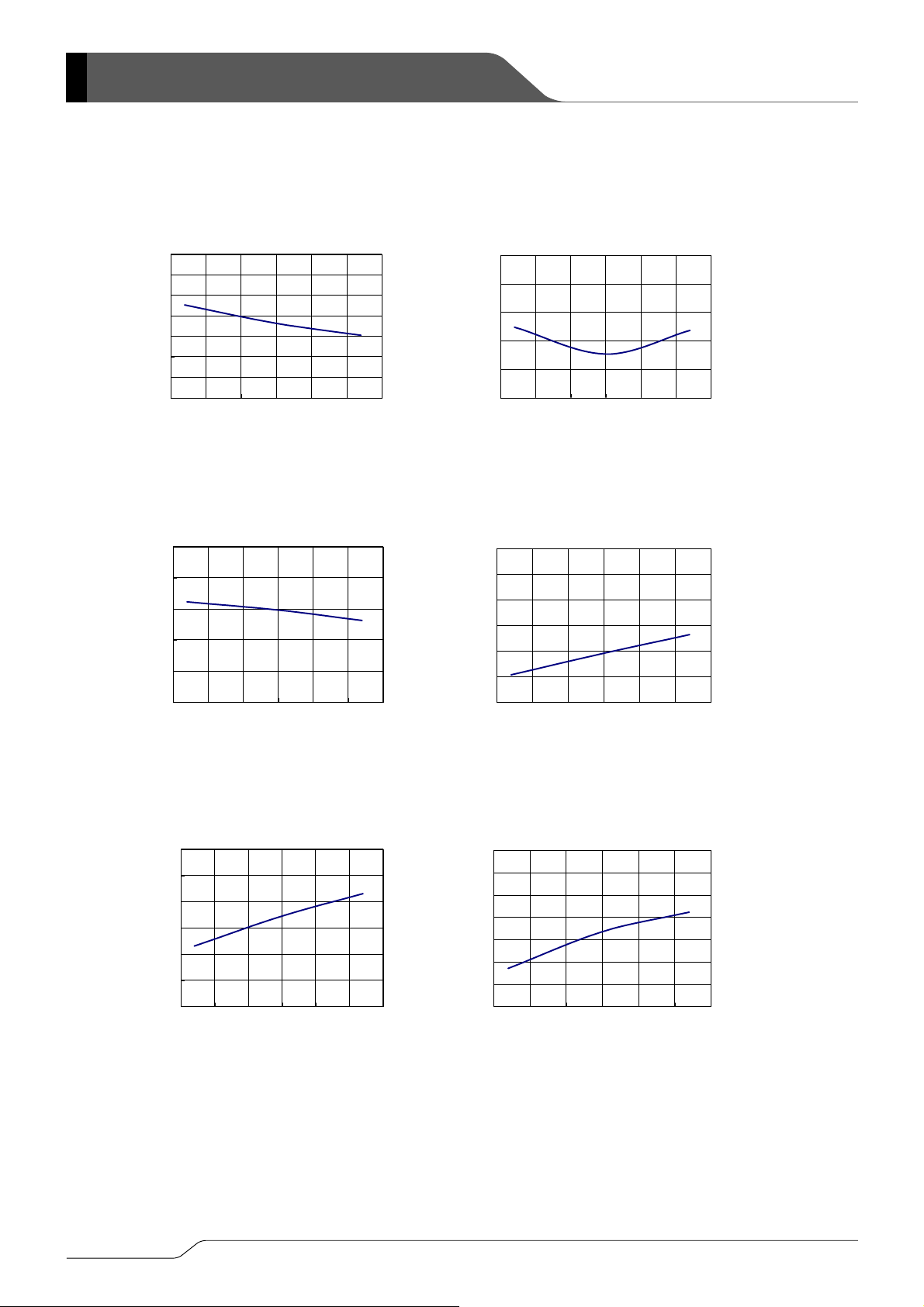
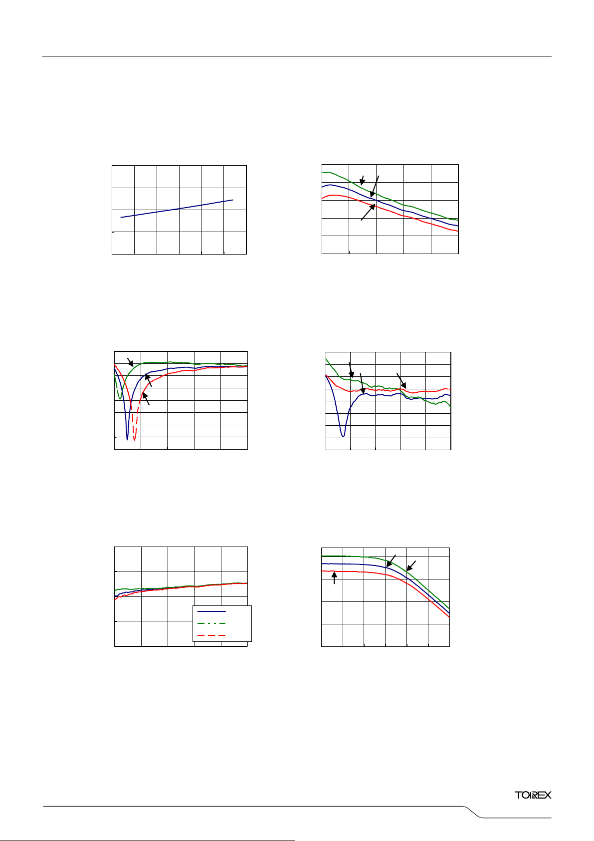
■TYPICAL PERFORMANCE CHARACTERISTICS
(1) Current Circuits vs. Supply Voltage
(1) 回路電流 - 電源端子電圧特性例
(3) CE “L” Level Voltage vs. Power Supply Voltage
(3) CE"L"レベル電圧 - 電源端子電圧特性例
(5) Input Return Loss vs. Power Supply Voltage
(5) 入力側リターンロス - 電源端子電圧特性例 (6) 出力側リターンロス - 電源端子電圧特性例
(V)
CEL
CE "L" Level Voltage : V
(mA)
DD
Current Circuits : I
Input Return Loss : S11 (dB)
8.5
8
7.5
7
6.5
6
5.5
5
1.1
1
0.9
0.8
0.7
0.6
0.5
0.4
-5
-5.5
-6
-6.5
-7
-7.5
-8
-8.5
-9
XC2408A816
VDD=VCE, Ta=25℃
2.6 2.7 2.8 2.9 3 3.1
Power Supply Voltage : V
(V)
DD
XC2408A816
Ta=25℃
2.6 2.7 2.8 2.9 3 3.1
Power Supply Voltage : V
(V)
DD
XC2408A816
VDD=VCE, Ta=25℃, f=1.575Hz
2.6 2.7 2.8 2.9 3 3.1
Power Supply Voltage : V
(V)
DD
(2) CE “H” Level Voltage vs. Supply Voltage
(2) CE"H"レベル電圧 - 電源端子電圧特性例
XC2408A816
1.1
(V)
1
CEH
0.9
0.8
0.7
0.6
0.5
0.4
2.6 2.7 2.8 2.9 3 3.1
CE "H" Level Voltage : V
Power Supply Voltage : V
(4) Power Gain vs. Power Supply Voltage
(4) 挿入電力利得 - 電源端子電圧特性例
XC2408A816
25
VDD=VCE, Ta=25℃, f=1.575Hz
24
23
22
21
20
Power Gain : S21 (dB)
19
2.6 2.7 2.8 2.9 3 3.1
Power Supply Voltage : V
(6) Output Return Loss vs. Supply Voltage
XC2408A816
VDD=VCE, Ta=25℃, f=1.575Hz
-15
-15.5
-16
-16.5
-17
-17.5
-18
Output Return Loss : S22 (dB)
2.6 2.7 2.8 2.9 3 3.1
Power Supply Voltage : V
Ta=25℃
(V)
DD
(V)
DD
(V)
DD
10/18

XC2408A816UR-G
■TYPICAL PERFORMANCE CHARACTERISTICS (Continued)
(7) Isolation vs. Power Supply Voltage
(7) アイソレーション - 電源端子電圧特性例 (8) 雑音指数 - 電源端子電圧特性例
(9) Input Power IP3 vs. Power Supply Voltage
(9) 入力IP3 - 電源端子電圧特性例 (10) 入力IP2 - 電源端子電圧特性例
(11) 1dB利得圧縮時入力電力 - 電源端子電圧特性例 (12) 挿入電力利得 - 周囲温度特性例
(11)
-30
-31
-32
-33
-34
Isolation : S12 (dB)
-35
-15
-15.2
-15.4
-15.6
-15.8
Input Power IP3 : IIP3 (dBm)
-16
Input Power @ 1dB Gain Compression vs. Power Supply Voltage
-21
-23
-25
: P1dB (dBm)
-27
-29
Input Power @ 1dB Gain Compression
XC2408A816
VDD=VCE, Ta=25℃, f=1.575Hz
2.6 2.7 2.8 2.9 3 3.1
Power Supply Voltage: V
(V)
DD
XC2408A816
VDD=VCE, Ta=25℃,
f=1.575GHz, 1.576GHz
2.6 2.7 2.8 2.9 3 3.1
Power Supply Voltage : V
(V)
DD
XC2408A816
VDD=VCE, Ta=25℃, f=1.575Hz
2.6 2.7 2.8 2.9 3 3.1
Power Supply Voltage: V
(V)
DD
(8) Noise Figure vs. Power Supply Voltage
XC2408A816
VDD=VCE, Ta=25℃, f=1.575Hz
1.6
1.4
1.2
1
0.8
0.6
Noise Figure : NF (dB)
0.4
2.6 2.7 2.8 2.9 3 3.1
Power Supply Voltage : V
(V)
DD
(10) Input Power IP2 vs. Power Supply Voltage
XC2408A816
15
14
13
12
11
Input Power IP2 : IIP2 (dBm)
10
2.6 2.7 2.8 2.9 3 3.1
Power Supply Voltage : V
VDD=VCE, Ta=25℃,
f=0.8GHz, 2.375GHz
(V)
DD
(12) Power Gain vs. Ambient Temperature
XC2408A816
VDD=VCE, Ta=25℃, f=1.575Hz
35
30
25
20
15
Power Gain : S21 (dB)
10
-50 -25 0 25 50 75 100
Ambient Temperature : Ta (℃)
11/18
XC2408A816UR-G
■TYPICAL PERFORMANCE CHARACTERISTICS (Continued)
(13) Input Return Loss vs. Ambient Temperature
(13) 入力側リターンロス - 周囲温度特性例 (14) 出力側リターンロス - 周囲温度特性例
(15) アイソレーション - 周囲温度特性例 (16) 雑音指数 - 周囲温度特性例
(15) Isolation vs. Ambient Temperature
(17) Input Power IP3 vs. Ambient Temperature
(17) 入力IP3 - 周囲温度特性例 (18) 入力IP2 - 周囲温度特性例
0
-2
-4
-6
-8
-10
-12
-14
Input Return Loss : S11 (dB)
-50 -25 0 25 50 75 100
-30
-31
-32
-33
-34
Isolation : S12 (dB)
-35
-14
-14.5
-15
-15.5
-16
-16.5
Input Power IP3 : IIP3 (dBm)
-17
XC2408A816
VDD=VCE, Ta=25℃, f=1.575Hz
Ambient Temperature : Ta (℃)
XC2408A816
VDD=VCE, Ta=25℃, f=1.575Hz
-50 -25 0 25 50 75 100
Ambient Temperature : Ta (℃)
XC2408A816
VDD=VCE=2.85V,
f=1.575GHz, 1.576GHz
-50 -25 0 25 50 75 100
Ambient Temperature : Ta (℃)
(14) Output Return Loss vs. Ambient Temperature
XC2408A816
VDD=VCE, Ta=25℃, f=1.575Hz
-10
-12
-14
-16
-18
-20
Output Return Loss : S22 (dB)
-50 -25 0 25 50 75 100
Ambient Temperature : Ta (℃)
(16) Noise Figure vs. Ambient Temperature
XC2408A816
3
2.5
2
1.5
1
0.5
Noise Figure : NF (dB)
0
-50 -25 0 25 50 75 100
Ambient Temperature : Ta (℃)
VDD=VCE, Ta=25℃, f=1.575Hz
(18) Input Power IP2 vs. Ambient Temperature
XC2408A816
VDD=VCE=2.85V,
20
18
16
14
12
10
8
Input Power IP2 : IIP2 (dBm)
6
-50 -25 0 25 50 75 100
Ambient Temperature : Ta (℃)
f=0.8GHz, 2.375GHz
12/18
: P1dB (dBm)
XC2408A816UR-G
■TYPICAL PERFORMANCE CHARACTERISTICS (Continued)
(19) 1dB利得圧縮時入力電力 - 周囲温度特性例 (20) 挿入電力利得 - 周波数特性例
(19) Input Power @ 1dB Gain Compression vs. Ambient Temperature
(21) 入力側リターンロス - 周波数特性例 (22) 出力側リターンロス - 周波数特性例
(21) Input Return Loss vs. Frequency
(23) Isolation vs. Frequency
(23) アイソレーション - 周波数特性例 (24) 挿入電力利得-入力電力特性例
: P1dB (dBm)
Input Power @ 1dB Gain Compression
Input Power @ 1dB Gain Compression
Input Return Loss : S11 (dB)
Isolation: S12 (dB)
-22
-23
-24
-25
-26
0
-5
-10
-15
-20
-25
-30
-35
-40
0
-20
-40
-60
-80
XC2408A816
VDD=VCE, Ta=25℃, f=1.575Hz
-50 -25 0 25 50 75 100
Ambient Temperature : Ta (℃)
XC2408A816
VDD=VCE=2.85V
-40℃
25℃
85℃
1 1.2 1.4 1.6 1.8 2
Frequency : f (GHz)
XC2408A816
VDD=VCE=2.85V
25℃
-40℃
85℃
1 1.2 1.4 1.6 1.8 2
Frequency: f (GHz)
(20) Power Gain vs. Frequency
XC2408A816
35
30
25
20
15
Power Gain : S21 (dB)
10
1 1.2 1.4 1.6 1.8 2
-40℃
25℃
85℃
Frequency : f (GHz)
(22) Output Return Loss vs. Frequency
XC2408A816
0
-40℃
-5
-10
-15
-20
-25
-30
-35
-40
Output Return Loss : S22 (dB)
1 1.2 1.4 1.6 1.8 2
25℃
Frequency : f (GHz)
85℃
(24) Power Gain vs. Input Power
XC2408A816
VDD=VCE=2.85V, f=1.575GHz
24
19
85℃
14
9
Power Gain : S21 (dB)
4
-40 -35 -30 -25 -20 -15 -10
Input Power : P
25℃
(dBm)
IN
VDD=VCE=2.85V
VDD=VCE=2.85V
-40℃
13/18
XC2408A816UR-G
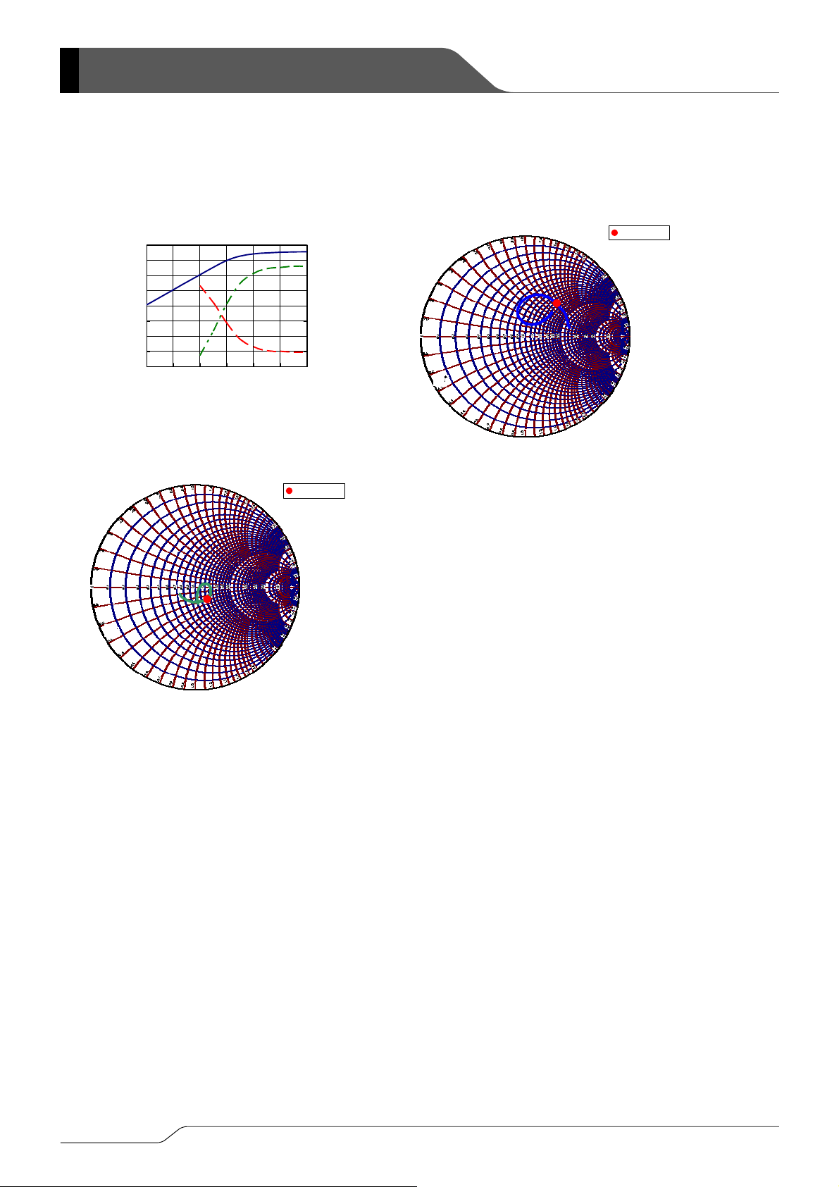
■TYPICAL PERFORMANCE CHARACTERISTICS (Continued)
(25) 出力電力/IM3 - 入力電力特性例 (26)入力側リターンロス -周波数特性例 (スミス図)
(25) Output Power / IM3 vs. Input Power
0
-10
(dBm)
-20
OUT
-30
-40
-50
-60
-70
-80
Output Power : P
-60 -50 -40 -30 -20 -10 0
XC2408A816
Desire
Undesire
Input Power : P
VDD=VCE=2.85V, Ta=25℃,
f=1.575GHz, 1.576GHz
IM3
(dBm)
IN
80
70
60
50
40
30
20
10
0
(27) Output Return Loss vs. Frequency (Smith Chart)
(27) 出力側リターンロス -周波数特性例 (スミス図)
XC2408A816
V
DD=VCE
f=1GHz~2GHz
=2.85V, Ta=25℃
f=1.575GHz
(26) Input Return Loss vs. Frequency (Smith Chart)
V
XC2408A816
Inter-Modulation distortion: IM3
DD=VCE
=2.85V, Ta=25℃
f=1GHz~2GHz
f=1.575GHz
14/18

XC2408A816UR-G
■PACKAGING INFORMATION
●USP-8A01 (unit:mm)
0.1±0.05 0.1±0.05
3
2
1
0.3±0.05 0.3±0.050.2±0.05
1.5±0.05
1PIN INDENT
4
5
6
7
8
15/18
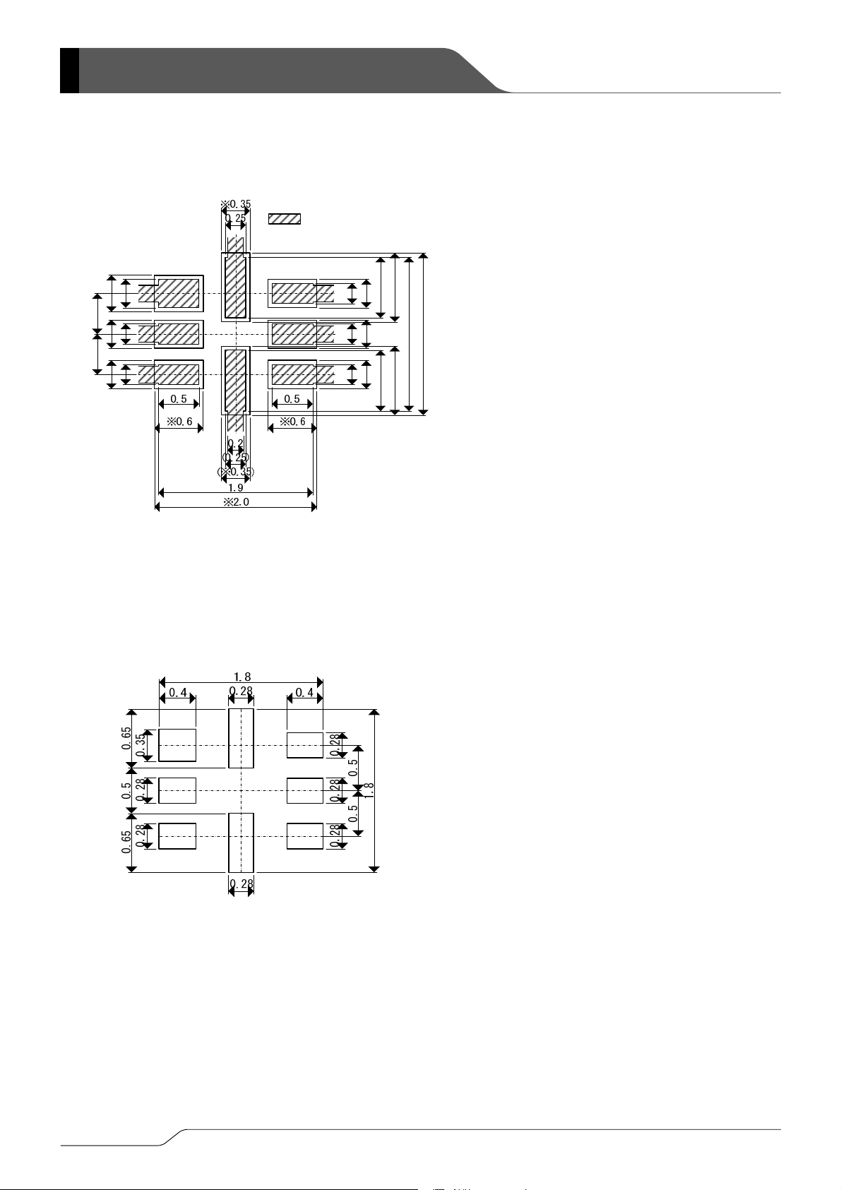
XC2408A816UR-G
■PACKAGING INFORMATION (Continued)
●USP-8A01Reference Pattern Layout (unit:mm)
※0.45※0.35※0.35
0.5 0.5
0.25 0.25 0.35
Mark ※ is opening of resist.
●USP-8A01Reference Metal Mask Design (unit:mm)
16/18
Is cupper area.
0.250.250.25
※0.35※0.35※0.35
0.75
0.75
※0.85 ※0.85
1.9
※2.0

XC2408A816UR-G
■MARKING RULE
USP-8A01
1
2
3
④ ⑤
8
① ② ③
7
6
5
4
① represents product series.
MARK PRODUCT SERIES
8 XC2408******-G
② represents product.
MARK
②
A XC2408A*****-G
③ represents product.
MARK
③
8 XC2408*8****-G
PRODUCT SERIES
PRODUCT SERIES
④,⑤ represents production lot number.
01 to 09, 0A to 0Z, 11 to 9Z, A1 to A9, AA to AZ and B1 to ZZ in order.
(G, I, J, O, Q, W excepted)
* No character inversion used.
17/18

XC2408A816UR-G
1. The products and product specifications contained herein are subject to change without
notice to improve performance characteristics. Consult us, or our representatives
before use, to confirm that the information in this datasheet is up to date.
2. We assume no responsibility for any infringement of patents, patent rights, or other
rights arising from the use of any information and circuitry in this datasheet.
3. Please ensure suitable shipping controls (including fail-safe designs and aging
protection) are in force for equipment employing products listed in this datasheet.
4. The products in this datasheet are not developed, designed, or approved for use with
such equipment whose failure of malfunction can be reasonably expected to directly
endanger the life of, or cause significant injury to, the user.
(e.g. Atomic energy; aerospace; transport; combustion and associated safety
equipment thereof.)
5. Please use the products listed in this datasheet within the specified ranges.
Should you wish to use the products under conditions exceeding the specifications,
please consult us or our representatives.
6. We assume no responsibility for damage or loss due to abnormal use.
7. All rights reserved. No part of this datasheet may be copied or reproduced without the
prior permission of TOREX SEMICONDUCTOR LTD.
18/18
 Loading...