


XC2401A8167R-G
ETR2701-004b
1.6 GHz Low Noise Amplifier
■GENERAL DESCRIPTION
The XC2401A8167R-G is an ultra-low-noise amplifier (LNA) with low operating voltage, low noise figure (NF), low power
consumption using CMOS process.
The device offers easy output matching to 50Ω for input and output with less external components.
An internal self bias function eliminates external bias setting.
The device operates at 1.2V. For higher power supplies such as 1.8V and 2.85V, the device can operate with a self bias of
one adding resister.
.
■APPLICATIONS
●GPS RF module
■TYPICAL APPLICATION CIRCUIT
Figure 1: Fixed Bias
■FEATURES
Noise Figure :NF=0.69dB(TYP.) (@ 1.575GHz)
Low Power Consumption :
6.6mW (TYP.) @ VDD=1.2V, Fixed Bias
High Gain :S21 =15dB(TYP.) (@ 1.575GHz)
Operation Voltage Range :1.14V~1.26V @ Fixed Bias
Output :CMOS Output, 50Ω driver built-in
Operating Ambient Temperature
:-40℃~+85℃
Package :USPN-4B02
Environmentally Friendly :EU RoHS Compliant, Pb Free
■ TYPICAL PERFORMANCE
CHARACTERISTICS
Figure 2: Self Bias
VIN [V] Rbias [Ω]
3.00 560
2.85 470
1.80 160
*
R
should be in ±1% tolerance and ±200ppm/℃ temperature stability.
BIAS
XC2401A816
17.0
16.0
15.0
14.0
13.0
S21 [dB]
12.0
11.0
10.0
1.375 1.475 1.575 1.675 1.775
Frequency [GHz]
VDD=1.2V Ta =25
℃
2.8
2.4
2
1.6
NF [dB]
1.2
0.8
0.4
0
1/16

XC2401A8167R-G
■PIN CONFIGURATION
■PIN ASSIGNMENT
PIN NUMBER
USPN-4B02
USPN-4B02
(BOTTOM VIEW)
PIN NAME FUNCTION
1 VDD Power Supply RF
2 RF_OUT RF Signal Output
3 VSS Ground
4 RF_IN RF Signal Input
■PRODUCT CLASSIFICATION
●Ordering Information
PRODUCT NAME PACKAGE ORDER UNIT
XC2401A8167R-G
(*1)
The “-G” suffix denotes Halogen and Antimony free as well as being fully RoHS compliant.
(*1)
USPN-4B02 5,000/Reel
2/16

■BLOCK DIAGRAM
■ABSOLUTE MAXIMUM RATINGS
Operating Ambient Temperature Topr
PAR AMETER SYMBOL RATINGS UNITS
Supply Voltage VDD
Supply Circuit IDD 30 mA
RF Input Power PIN 10 dBm
RF_IN Input Voltage RF_IN
RF_OUT Input Voltage RF_OUT
Power Dissipation Pd 100 mW
Storage Temperature Tstg
V
SS
- 0.3 ~ V
V
SS
- 0.3 ~ V
V
SS
-55~+125
- 0.3 ~ 1.60
+ 0.3
DD
+ 0.3
DD
-40~+85
XC2401A8167R-G
Ta =2 5℃
V
V
V
o
C
o
C
3/16

)
XC2401A8167R-G
■ELECTRICAL CHARACTERISTICS
●DC Characteristics
4/16
Fixed Bias (refer to TYPICAL APPLICATION CIRCUIT, Figure 1)
PAR AMETER SYMBOL
Power Supply Pin Voltage VDD - 1.14 1.20 1.26 V ①
Current Circuit IDD V
CONDITIONS MIN. TYP. MAX. UNITS CIRCUIT
=1.2V 5.5 10.5
DD
Self Bias (refer to TYPICAL APPLICATION CIRCUIT,Figure 2
PAR AMETER SYMBOL
Input Power Supply
Voltage 1
Input Power Supply
Voltage 2
Input Power Supply
Voltage 3
V
IN1
V
IN2
V
IN3
Power Supply Pin Voltage VDD V
Current Circuit IDD V
* When the device is used in self bias, please use the specified R
CONDITIONS MIN. TYP. MAX. UNITS CIRCUIT
Rbias=560Ω±1%
±200ppm/℃
Rbias=470Ω±1%,
±200ppm/℃
Rbias=160Ω±1%,
±200ppm/℃
= V
= V
IN1
IN1
, V
, V
IN
IN
2.850 3.000 3.150 V ①
2.708 2.850 2.992 V ①
1.710 1.800 1.890 V ①
, V
0.90 1.12 1.32 V ①
IN2
IN3
, V
- 4.25 5.50 mA ①
IN2
IN3
BIAS
and C
BIAS
.
mA
Ta =2 5℃
①

●
■ELECTRICAL CHARACTERISTICS (Continued)
AC Characteristics
XC2401A8167R-G
V
=1.2V Ta=25℃
DD
PAR AMETER SYMBOL
CONDITIONS MIN. TYP. MAX. UNITS CIRCUIT
Power Gain S21 f=1.575 GHz 11.5 15.0 - dB ②
Input Return Loss S11 f=1.575GHz - 6 -
Output Return Loss S22 f=1.575GHz - 6 -
Isolation S12 f=1.575GHz - -20 -
Noise Figure
Input Power IP3 I
Input Power @ 1dB
Gain Compression
*1: NF is the value excluding the PCB loss.
Note
1. In case symptoms of transient voltage drop and rise temporarily, please use this IC within the stated maximum ratings.
The IC is liable to malfunction should the ratings be exceeded.
2. Please eliminate static electricity from the operational table, people, and soldering iron.
3. Please use noiseless power supply for stable operation.
4. Please use ±1% Rbias with ±200ppm/℃ temperature stability and 10nF Cbias.
5. Please connect Cbias to V
6. Please ensure to use an external component which does not depend on bias or temperature too much.
7. We will improve the product quality and improve reliability, however please make sure to design fail safe or pre-aging treatment on
the system.
(*1)
NF f=1.575GHz - 0.69 - dB ③
IP3
f=1.575GHz, 1.576GHz
Pin = -30dBm
- -1.0 - dBm ④
P1dB f=1.575GHz - -12 - dBm ②
pin as close as possible.
DD
dB
dB
dB
②
②
②
5/16

XC2401A8167R-G
■TEST CIRCUITS
●Circuit ① (DC Characteristics: Power Supply Pin Voltage, Circuit Current, Input Power Supply Voltage)
●Circuit ② (Power Gain, Input Return Loss, Output Return Loss, Isolation, Input Power @ 1dB Gain Compression)
* Fixed Bias: Rbias=0Ω, VIN=V
** Pin / Pout is 50Ω
DD
●Circuit ③ (Noise Figure)
6/16
*1: Refer to the circuit ⑤ for the block detail.
*1: Refer to the circuit ⑤ for the block detail.

■TEST CIRCUITS (Continued)
●Circuit ④ (Input Power IP3)
●Circuit ⑤ (XC2401 series, the circuit of the block)
*1: Refer to the circuit⑤for the block detail.
XC2401A8167R-G
VIN(V)
3.00 560
2.85 470
1.80 160
Rbias(Ω)
100pF
RF_OUTRF_IN
Rbias
V
DD
V
IN
Cbias=10nF
* Fixed Bias: Rbias=0Ω, VIN=V
** Rbias: Should be in ±1% tolerance and ±200ppm/℃ temperature stability.
V
SS
DD
7/16

XC2401A8167R-G
■EVALUATION BOARD
18mm
V
DD
V
SS
R1
C2
L1L2C1
PinPout
20mm
SYMBOL SPEC COMMENT
C1 100pF
C2 10nF -
L1 9.1nH
L2 6.2nH
R1
(Rbias)
(*1)
(*1)
Less than
MURATA
(GRM1552C1H)
TDK
(GLQ1005type)
TDK
( GLQ1005type)
Less than ±1% tolerance,
±200ppm/℃ temperature stability
PCB(FR-4)
MICROSTRIPLINE WIDTH = 0.6mm
t = 0.018mm
PCB size = 20mm×18mm
*1: Fixed Bias: Rbias=0Ω
* Please use an external component which does
not depend on bias or temperature too much.
8/16

■TYPICAL PERFORMANCE CHARACTERISTICS
(1) Supply Circuit vs. Supply Voltage
(2) Power Gain vs. Supply Voltage
XC2401A8167R-G
XC2401A816
Ta=25
℃
12.0
10.0
8.0
6.0
4.0
2.0
Supply Current: IDD (mA)
0.0
1.12 1.14 1.16 1.18 1.2 1.22 1.24 1.26 1.28
Supply Voltage: V
(V)
DD
(3) Input Return Loss vs. Supply Voltage
16.5
16.0
15.5
S21(dB)
:
15.0
14.5
14.0
Power G ian
13.5
1.12 1.14 1.16 1.18 1.2 1.22 1.24 1.26 1.28
(4) Output Return Loss vs. Supply Voltage
XC2401A816
Ta=25℃、Pin= -35dBm
-4.5
-5.0
S11 (dB)
-5.5
:
-5.0
-5.5
S22 (dB)
:
-6.0
XC2401A816
Supply Voltage: V
XC2401A816
Ta=25℃、Pin= -35dBm
(V)
DD
Ta=25℃、Pin= -35dBm
-6.0
-6.5
-7.0
Intput Return Loss
-7.5
1.12 1.14 1.16 1.18 1.2 1.22 1.24 1.26 1.28
Supply Voltage: V
DD
(V)
(5) Reverse Isolation vs. Supply Voltage
XC2401A816
Ta=25℃、Pin= -35dBm
-21.0
-21.5
S12 (dB)
-22.0
:
-22.5
-23.0
-23.5
-6.5
-7.0
-7.5
Outtput Return Los s
-8.0
1.12 1.14 1.16 1.18 1.2 1.22 1.24 1.26 1.28
Supply Voltage: V
DD
(6) Noise Figure vs. Supply Voltage
XC2401A816
Ta=25℃、f=1.575GH z
1.2
1.0
0.8
0.6
0.4
Noise Figure: NF (dB)
0.2
(V)
Reverse Isolation
-24.0
1.12 1.14 1.16 1.18 1.2 1.22 1.24 1.26 1.28
Supply Voltage: V
DD
(V)
0.0
1.12 1.14 1.16 1.18 1.2 1.22 1.24 1.26 1.28
Supply Voltage: V
DD
(V)
9/16

XC2401A8167R-G
■TYPICAL PERFORMANCE CHARACTERISTICS (Continued)
(7) Input 3 Order Intercept Point vs. Supply Voltage
XC2401A816
0.0
VD D= 1.2V,Pin= -30dBm
f =1.575&1.576GH z
(8) Input Power @ 1dB Gain compression vs. Power Supply Voltage
XC2401A816
Ta=25℃、f=1.575GH z
-10.5
-0.2
-0.4
-0.6
IIP3(dBm)
-0.8
-1.0
Input 3Order Intercept Point:
-1.2
-50 -25 0 25 50 75 100
Ambient Temperature:Ta(℃)
(9) Supply Current vs. Ambient Temperature
XC2401A816
VDD=1.2V
12.0
10.0
8.0
6.0
4.0
Input Power @1dB Gian
-11.0
-11.5
-12.0
-12.5
-13.0
Compres sion: P1dB (dBm)
-13.5
1.12 1.14 1.16 1.18 1.2 1.22 1.24 1.26 1.28
Supply Voltage: V
DD
(10) Power Gain vs. Ambient Temperature
XC2401A816
VDD= 1.2V Pin= -35dBm
16.5
16.0
15.5
S21(dB)
:
15.0
14.5
(V)
Supply Current: IDD (mA)
S11 (dB)
:
Intput Return Loss
10/16
2.0
0.0
-50 -25 0 25 50 75 100
Ambient Temperature:Ta(℃)
(11) Input Return Loss vs. Ambient Temperature
XC2401A816
VD D= 1.2V Pin= -35dBm
-4.5
-5.0
-5.5
-6.0
-6.5
-7.0
-7.5
-50 -25 0 25 50 75 100
Ambient Temperature:Ta(℃)
14.0
Power G ian
13.5
-50 -25 0 25 50 75 100
Ambient Temperature:Ta(℃)
(12) Output Return Loss vs. Ambient Temperature
XC2401A816
VDD= 1. 2V Pin=- 35dBm
-5.0
-5.5
S22 (dB)
:
-6.0
-6.5
-7.0
-7.5
-8.0
Outtput Return Los s
-50 -25 0 25 50 75 100
Ambient Temperature:Ta(℃)

XC2401A8167R-G
■TYPICAL PERFORMANCE CHARACTERISTICS (Continued)
(13) Reverse Isolation vs. Ambient Temperature
(14) Noise Figure vs. Ambient Temperature
XC2401A816
-21.0
-21.5
-22.0
-22.5
-23.0
-23.5
Reverse Isolation: S12 (dB)
-24.0
-50 -25 0 25 50 75 100
Ambient Temperature:Ta(℃)
Input 3 Order intercept point vs. Ambient Temperature
(15)
XC2401A816
0.0
-0.2
-0.4
-0.6
IIP3(dBm)
-0.8
-1.0
Input 3Order Intercept Point:
-1.2
1.12 1.14 1.16 1.18 1.2 1.22 1.24 1.26 1.28
Supply Voltage: V
(17) Power Gain vs. Frequency
VDD= 1.2V Pin= -35dBm
Ta=25℃,Pin= -30dBm
f =1.575&1.576GH z
(V)
DD
1.2
1.0
0.8
0.6
0.4
0.2
Noise Figure: NF (dB)
0.0
-50 -25 0 25 50 75 100
(16)
Input Power @ 1dB Gain Compression vs. Ambient Temperature
-10.5
-11.0
-11.5
-12.0
-12.5
-13.0
Input Power @1dB Gian
Compression: P1dB (dBm)
-13.5
-50 -25 0 25 50 75 100
(18) Input Return Loss vs. Frequency
XC2401A816
VD D=1.2V、f = 1.575GH z
Ambient Temperature:Ta(℃)
XC2401A816
VD D= 1.2V Pin= -35dBm
Ambient Temperature:Ta(℃)
XC2401A816
VDD= 1. 20V Pin=- 35dBm
20
18
f[GHz]
:
-40
16
S21(dB)
:
14
12
Power G ian
10
8
1.00 1.20 1.40 1.60 1.80 2.00
25
℃
Frequency
85
℃
℃
XC2401A816
VDD= 1.20V Pin= -35dBm
-1.5
-2.5
S11 (dB)
-3.5
:
-4.5
85
-5.5
-6.5
Intput Return Loss
-7.5
1.00 1.20 1.40 1.60 1.80 2.00
25
℃
℃
Frequency
f[GHz]
:
-40
℃
11/16

XC2401A8167R-G
■TYPICAL PERFORMANCE CHARACTERISTICS (Continued)
(19) Output Return Loss vs. Frequency
XC2401A816
VDD= 1.20V Pin= -35dBm
-4
-5
S22 (dB)
-6
:
-7
-8
25
f[GHz]
:
℃
-9
Outtput Return Los s
-10
1.00 1.20 1.40 1.60 1.80 2.00
Frequency
(21) Noise Figure vs. Frequency
-20
-21
-22
S12 (dB)
:
-23
85
℃
-40
℃
-24
-25
Reverse Isolation
-26
(20) Isolation vs. Frequency
XC2401A816
VDD= 1. 20V Pin=- 35dBm
85
℃
25
℃
-40
℃
1.00 1.20 1.40 1.60 1.80 2.00
Frequency
f[GHz]
:
(22) Power Gain vs. Input Power
XC2401A816
VDD= 1.20V Pin= -35dBm
6
5
4
3
25
2
Noise Figure: NF (dB)
1
0
1.00 1.20 1.40 1.60 1.80 2.00
℃
Frequency
-40
℃
f[GHz]
:
85
(23) Output Power / IM3 vs. Input Power
XC2401A816
20
0
-20
Des ire
℃
VDD=1.2V、Ta=25
XC2401A816
VDD= 1.20V , f= 1.575GH z
18
-40
16
14
25
℃
12
Power Gian :P(dB)
10
8
-40 -35 -30 -25 -20 -15 -10 -5
℃
85
℃
Input Pow er:Pin(dBm)
℃
120
100
80
-40
-60
-80
Output Power:Pout(dBm)
-100
12/16
Undesire
IM3
-50 -40 -30 -20 -10 0 10
Input Pow er: Pin(dBm)
60
IM3(dB)
40
20
Inter-Modulation distortion:
0

XC2401A8167R-G
■TYPICAL PERFORMANCE CHARACTERISTICS (Continued)
(24) Input Return Loss vs. Frequency (Smith Chart)
XC2401A816
VDD=1.2V, Pin=-35dBm
(25) Output Return Loss vs. Frequency (Smith Chart)
XC2401A816
VDD=1.2V, Pin=-35dBm
1.575GHz
1.575GHz
13/16
XC2401A8167R-G
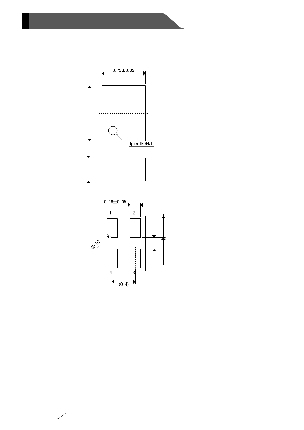
■ PACKAGING INFORMATION
●USPN-4B02
0.95±0.05
-0.03
+0.02
0.38
0.325±0.05
0.2±0.05
14/16

■ PACKAGING INFORMATION (Continued)
●USPN-4B02 Reference Pattern Layout
XC2401A8167R-G
●USPN-4B02 Reference Metal Mask Design
■MARKING RULE
USPN-4B02
43
① ②
③
1
2
0.50.2
① represents product series.
MARK PRODUCT SERIES
0.350.35
8 XC2401******-G
② represents product.
MARK PRODUCT SERIES
A XC2401A816**-G
③ represents production lot number.
01 to 09, 0A to 0Z, 11 to 9Z, A1 to A9, AA to Z9, ZA to ZZ in order.
(G, I, J, O, Q, W excepted)
*No character inversion used.
15/16

XC2401A8167R-G
1. The products and product specifications contained herein are subject to change without
notice to improve performance characteristics. Consult us, or our representatives
before use, to confirm that the information in this datasheet is up to date.
2. We assume no responsibility for any infringement of patents, patent rights, or other
rights arising from the use of any information and circuitry in this datasheet.
3. Please ensure suitable shipping controls (including fail-safe designs and aging
protection) are in force for equipment employing products listed in this datasheet.
4. The products in this datasheet are not developed, designed, or approved for use with
such equipment whose failure of malfunction can be reasonably expected to directly
endanger the life of, or cause significant injury to, the user.
(e.g. Atomic energy; aerospace; transport; combustion and associated safety
equipment thereof.)
5. Please use the products listed in this datasheet within the specified ranges.
Should you wish to use the products under conditions exceeding the specifications,
please consult us or our representatives.
6. We assume no responsibility for damage or loss due to abnormal use.
7. All rights reserved. No part of this datasheet may be copied or reproduced without the
prior permission of TOREX SEMICONDUCTOR LTD.
16/16
 Loading...