


■
■
A
■
■
■
XC2300 Series
ETR1406_001a
Tri-State Buffer ICs
GENERAL DESCRIPTIO N
The 2300 Series are a group of high frequenc y, CMOS low power tri-state buffer ICs with input amplifier, divider and output
tri-state buffer circuits built-in.
The series is available in an ultra small SOT-26 package.
PPLICATIONS
●VCXO modules
●Crystal oscillator modules
PIN CONFIGURATION
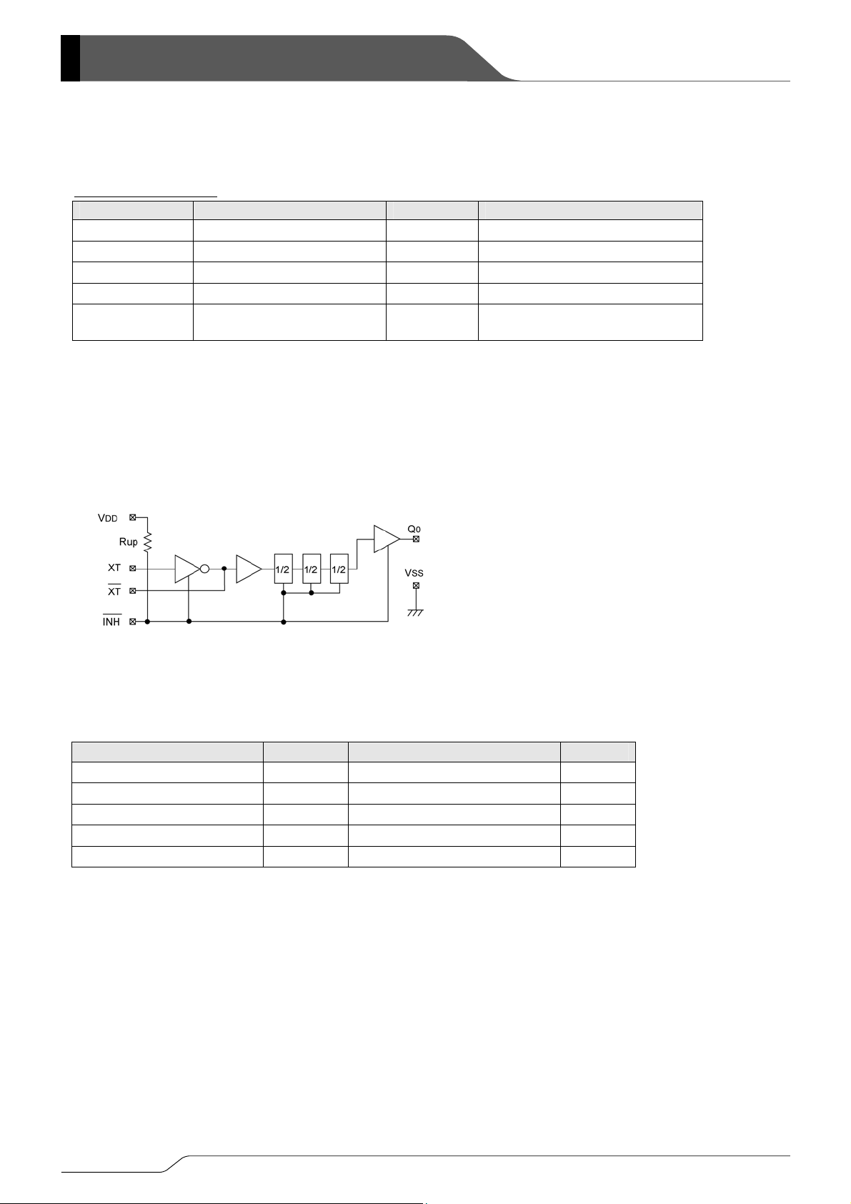
/INH, Q0 PIN FUNCTION
/INH Q0
“H” or OPEN Clock Output
“L” High Impedance
FEATURES
Max. Operating Frequency
Operating Voltage Range
Divider Ratio
Output
CMOS Low Power Consumption
Built-In Input Amplifier
Ultra Small Package
Environmentally Friendly
: 70MHz
3.3V±10%, 5.0V±20%
:
: fin/1
: 3-State
: SOT-26
: EU RoHS Compliant, Pb Free
■PIN ASSIGNMENT
PIN
NUMBER
1 /INH Stand-by Control (*)
2 XT Clock Input
3 VSS Ground
4 Q0 Clock Output
5 VDD Power Supply
6 /XT
*Stand-by control pin has a pull-up resistor built-in.
PIN
NAME
FUNCTION
Feedback Resistor Connection
(Output)
1/7
■
■
■
A
r
XC2300 Series
PRODUCT CLASSIFICATION
●Ordering Information
XC2300①②③④⑤⑥‑⑦
DESTINATOR
①
②
③
④
⑤⑥‑⑦
(*1)
The “-G” suffix indicates that the products are Halogen and Antimony free as well as being fully RoHS compliant.
(*2)
The device orientation is fixed in its embossed tape pocket. For reverse orientation, please contact your local Torex sales office o
representative. (Standard orientation: ⑤R-⑦, Reverse orientation: ⑤L-⑦)
(*1)
DESCRIPTION SIMBOL DESCRIPTION
Duty Level C : CMOS (V
Fixed Number 2
Divider Ratio 1
Output V
Packages
Taping Type
(*2)
MR-G : SOT-26
: : Q0=fin/1
: Tri-state buffer
DD/2)
BLOCK DIAGRAM
BSOLUTE MAXIMUM RATINGS
PARAMETER SYMBOL CONDITIONS UNITS
Supply Voltage VDD VSS - 0.3 ~ VSS + 7.0 V
Input Voltage VIN VSS - 0.3 ~ VDD + 0.3 V
Power Dissipation Pd 250(**) mW
Operating Temperature Range Topr - 40 ~ + 85
Storage Temperature Range Tstg
- 55 ~ + 125
** When implemented on a glass epoxy PCB.
Ta=25℃
℃
℃
2/7
■
XC2300
Series
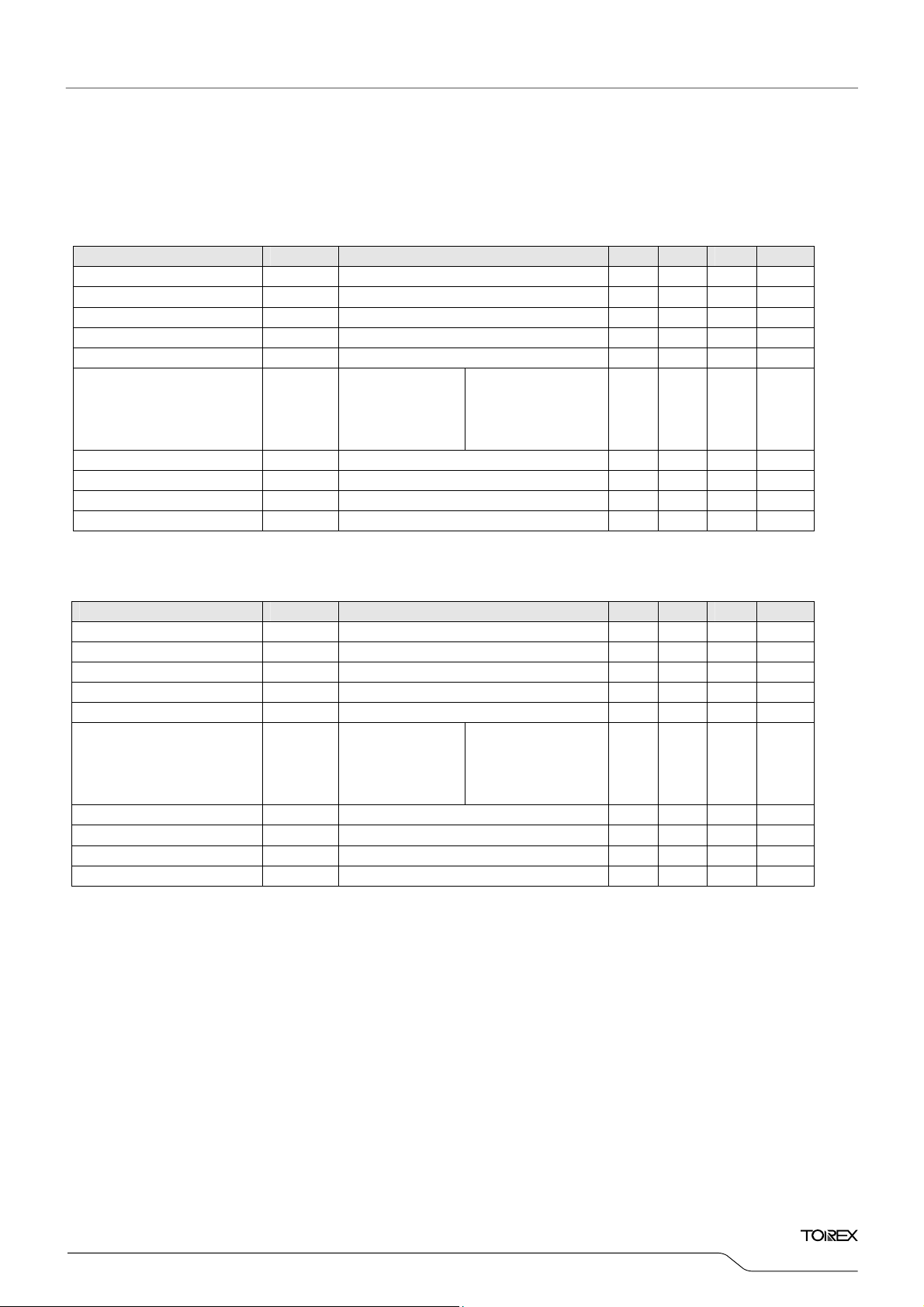
ELECTRICAL CHARACTERISTICS
●DC Electrical Characteristics
5.0V operation
PARAMETER SYMBOL CONDITIONS MIN. TYP. MAX. UNITS
Operating Supply Voltage VDD 4.0 5.0 6.0 V
Input Voltage "High" VIH /INH pin 2.4 - - V
Input Voltage "Low" VIL /INH pin - - 0.4 V
Output Voltage "High" VOH Q0 pin, VDD=4.5V, IOH= -8mA 3.9 4.2 - V
Output Voltage "Low" VOL Q0 pin, VDD=4.5V, IOL=8mA - 0.3 0.4 V
NH=OPEN,
/I
Supply Current 1 IDD1
Supply Current 2 IDD2 /INH="L", fin=70MHz - 0.05 - mA
Input Pull-Up Resistance 1 Rup1 /INH="L" 2.0 4.0 8.0
Input Pull-Up Resistance 2 Rup2 /INH=0.7VDD 50 100 200
Output Off Leak Current IOZ Q0 pin, /INH="L" - - 10
Q
0=OPEN
Fin=70MHz
(Unless otherwise stated, VDD=5.0V, No Load, Ta=25℃)
XC2300C21V (fin/1) - 21.0 - mA
MΩ
kΩ
μA
3.3V operation
PARAMETER SYMBOL CONDITIONS MIN. TYP. MAX. UNITS
Operating Supply Voltage VDD 2.97 3.30 3.63 V
Input Voltage "High" VIH /INH pin 2.4 - - V
Input Voltage "Low" VIL /INH pin - - 0.4 V
Output Voltage "High" VOH Q0 pin, VDD=4.5V, IOH= -4mA 2.2 2.4 - V
Output Voltage "Low" VOL Q0 pin, VDD=4.5V, IOL=4mA - 0.3 0.4 V
NH =OPEN,
/I
Supply Current 1 IDD1
Supply Current 2 IDD2 /INH ="L", fin=50MHz - 0.05 - mA
Input Pull-Up Resistance 1 Rup1 /INH ="L" 4.0 7.0 14.0
Input Pull-Up Resistance 2 Rup2 /INH =0.7VDD 70 130 250
Output Off Leak Current IOZ Q0 pin, /INH ="L" - - 10
Q
0=OPEN
Fin=50MHz
(Unless otherwise stated, V
XC2300C21V (fin/1) - 8.0 - mA
DD=3.3V, No Load, Ta=25℃)
MΩ
kΩ
μA
3/7

)
■
XC2300 Series
ELECTRICAL CHARACTERISTIC (Continued)
●AC Electrical Characteristics
5.0V operation
PARAMETER SYMBOL CONDITIONS MIN. TYP. MAX. UNITS
Maximum Operating Frequency fmax 70 - - MHz
5.0V operation (Reference value
PARAMETER SYMBOL CONDITIONS MIN. TYP. MAX. UNITS
Input Amplitude (SIN wave) Vipp 0.5 - - Vpp
Output Duty Cycle (*1) DUTY fin=70MHz, CL=15pF, Vipp=0.5Vpp 45 - 55 %
Output Rise Time (*2) tr fin=70MHz, CL=15pF, Vipp=0.5Vpp - (3.0) 5.0 ns
Output Fall Time (*3) tf fin=70MHz, CL=15pF, Vipp=0.5Vpp - (1.5) 5.0 ns
*1) 0.5VDD
DD→0.9VDD
*2) 0.1V
DD→0.1VDD
*3) 0.9V
(Unless otherwise stated, VDD=5.0V, No Load, Ta=25℃)
(Unless otherwise stated, VDD=5.0V, No Load, Ta=25℃)
3.3V operation
PARAMETER SYMBOL CONDITIONS MIN. TYP. MAX. UNITS
Maximum Operating Frequency fmax 50 - - MHz
(Unless otherwise stated, V
DD=3.3V, No Load, Ta=25℃)
3.3V operation (Reference value)
PARAMETER SYMBOL CONDITIONS MIN. TYP. MAX. UNITS
Input Amplitude (SIN wave) Vipp 0.5 - - Vpp
Output Duty Cycle (*1) DUTY fin=50MHz, CL=15pF, Vipp=0.5Vpp 45 - 55 %
Output Rise Time (*2) tr fin=50MHz, CL=15pF, Vipp=0.5Vpp - (4.0) 8.0 ns
Output Fall Time (*3) tf fin=50MHz, CL=15pF, Vipp=0.5Vpp - (2.0) 8.0 ns
*1) 0.5VDD
DD→0.9VDD
*2) 0.1V
*3) 0.9V
DD→0.1VDD
(Unless otherwise stated, VDD=3.3V, No Load, Ta=25℃)
4/7

■
■
SWITCHING WAVEFORMS
(1) Switching Time
(2) Duty Cycle
SUPPLY CURRENT, DUTY TEST CIRCUIT
*) The feedback resistor (fixed) Rf must be connected.
*) When the duty needs to be adjusted because of power
supply and/or input amplitude, duty resistor (fixed) Rb
should be connected.
<Reference Peripheral Values: Rf, Rb, C
V
DD=5.0V, fin=70MHz, Vipp=0.5Vpp
C
IN = 10000 [pF]
IN>
Rf = 100 [kΩ]
Rb = 720 [kΩ]
V
DD=3.3V, fin=50MHz, Vipp=0.5Vpp
C
IN = 10000 [pF]
Rf = 100 [kΩ]
Rb = 820 [kΩ]
XC2300
Series
5/7

■
■
p
XC2300 Series
PACKAGING INFORMATION
●SOT-26
MARKING RULE
●SOT-26
654
① ② ③ ④
123
(Based on internal standards)
①Represents product series
MARK PRODUCT SERIES
0 XC2300xxxxxx
resents divider ratio
②Re
MARK RATIO
C fin/1
③Represents tri-state buffer ICs
MARK
V
④Represents assembly lot number
6/7

XC2300
Series
1. The products and prod uct specifications cont ained herein are subject to change without
notice to improve performance characteristics. Consult us, or our representatives
before use, to confirm that the information in this datasheet is up to date.
2. We assume no responsibility for any infringement of patents, patent rights, or other
rights arising from the use of any information and circuitry in this datasheet.
3. Please ensure suitable shipping controls (including fail-safe designs and aging
protection) are in force for equipment employing products listed in this datasheet.
4. The products in this datasheet are not developed, designed, or approved for use with
such equipment whose failure of malfunction can be reasonably expected to directly
endanger the life of, or cause significant injury to, the user.
(e.g. Atomic energy; aerospace; transport; combustion and associated safety
equipment thereof.)
5. Please use the products listed in this datasheet within the specified ranges.
Should you wish to use the products under conditions exceeding the specifications,
please consult us or our representatives.
6. We assume no responsibility for damage or loss due to abnormal use.
7. All rights reserved. No part of this datasheet may be copied or reproduced without the
prior permission of TOREX SEMICONDUCTOR LTD.
7/7
 Loading...