

A
XC221A Series
ETR1201_002
1.2V Input / Output Rail To Rail CMOS Op Amp
■GENERAL DESCRIPTIO N
The XC221A series is an input / output rail to rail CMOS Op Amp.
With rail to rail functions, operation is guaranteed from power supplies a s low as 1.2V. Moreover, since the XC221A series
comes in an ultra small SOT-25 package, the series is particularly suited for use with various types of portable phones.
Bandwidths of 550kHz and slew rates of 0.5V can be achieved even with power consumption as low as 100μA.
Even with large capacitance levels of CL = 200pF (unity gain connection), the XC221A series will not be susceptible to
oscillation.
■
●Palmtop computers, PDAs
●Cellular and portable phones
●Portable audio systems
●Various battery powered systems
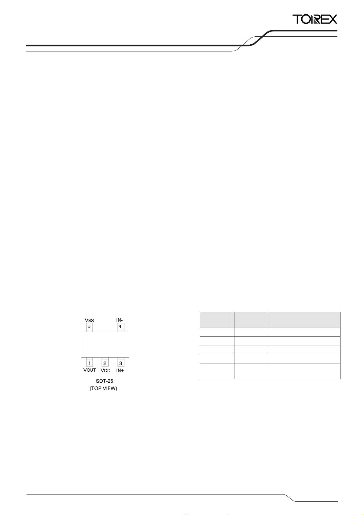
■PIN CONFIGURATION
PPLICATIONS
■FEATURES
Operating Voltage Range:1.2 ~ 10V (single cell)
:±0.6 ~ 5V (+ve/-ve supply)
Output Signal :0.1~2.9V (3V single cell, RL=2kΩ)
Gain Bandwidth :550kHz (15μA: 210kHz)
Slew Rate :0.5V/μs
High Capacitance Load :CL=200pF
Low Supply Current :100μA, 15μA
Input / Output Rail To Rail Operation
Package :SOT-25
Environmentally Friendly:EU RoHS Compliant, Pb Free
■PIN ASSIGNMENT
PIN
NUMBER
1 VOUT Output Pin
2 VDD Positive Power Supply Pin
3 IN+ Positive Input
4 IN- Negative Input
5 VSS
SYMBOL FUNCTION
Negative
Power Supply Pin
1/9
A
r
XC221A Series
■PRODUCT CLASSIFICATION
●Ordering Information
XC221A①②③④⑤⑥-⑦
DESIGNATOR DESCRIPTION SYMBOL DESCRIPTION
①
②
③
④
⑤⑥-⑦
(*1)
The “-G” suffix indicates that the products are Halogen and Antimony free as well as being fully RoHS compliant.
(*2)
The device orientation is fixed in its embossed tape pocket. For reverse orientation, please contact your local Torex sales office o
representative. (Standard orientation: ⑤R-⑦, Reverse orientation: ⑤L-⑦)
■
BSOLUTE MAXIMUM RATINGS
PARAMETER SYMBOL RATINGS UNITS
VDD Pin Voltage VDD
OUT Pin Voltage VOUT
IN Pin Voltage VIN+
IN/ Pin Voltage VIN-
OUT Pin Current IOUT
Power Dissipation Pd 150 mW
Operating Temperature Range Topr
Storage Temperature Range Tstg
RAIL-TO-RAIL is a trademark of Motorola.
(*1)
The Number of Channels 1 One channel
Supply Current
Internal Standard Number 0 Fixed
Load Capacitance 0 200pF
Packages
Taping Type
(*2)
1
2
MR SOT-25
MR-G SOT-25 (Halogen & Antimony free)
15μA
100μA
-0.3 ~ 12.0
-0.3 ~ 12.0
-0.3~V
-0.3~V
DD+0.3
DD+0.3
±100
-30 ~ +80 ℃
-40 ~ +125 ℃
Ta = 25℃, VSS = 0V
V
V
V
V
mA
2/9

μ
XC221A
■ELECTRICAL CHARACTERISTICS
XC221A1100
PARAMETER SYMBOL CONDITIONS MIN. TYP. MAX. UNITS
Supply Voltage VDD 1.2 - 10.0 V
Supply Current IDD
Input Offset Voltage VOF - - 20.0 mV
Input Offset Current IOF - 1 - pA
Input Bias Current IB - 1 - pA
Input Resistance RIN - 1 -
Large Signal Voltage Gain AVD 75 110 - dB
Common Mode
Rejection Ratio
Rejection Ratio
Output Voltage Range VOUT
Gain Bandwidth FT VDD = 3V - 210 - kHz
Slew Rate SR VDD = 3V - 0.07 -
Test Conditions :Unless otherwise stated, V
XC221A1200
PARAMETER SYMBOL CONDITIONS MIN. TYP. MAX. UNITS
Supply Voltage VDD 1.2 - 10.0 V
Supply Current IDD
Input Offset Voltage VOF - - 20.0 mV
Input Offset Current IOF - 1 - pA
Input Bias Current IB - 1 - pA
Input Resistance RIN - 1 -
Large Signal Voltage Gain
Common Mode
Rejection Ratio
Power Supply Rejection
Ratio
Output Voltage Range VOUT
Gain Bandwidth FT VDD = 3V - 550 - kHz
Slew Rate SR VDD = 3V - 0.50 -
Test Conditions :Unless otherwise stated, VDD = 3.0V, VSS = 0V, VCM = VOUT = VDD / 2, RL = 1MΩ (to VSS), CL = 10pF (to VSS)
I
DD =15
IDD =100μA
A
VDD = 3V 10 15 23
DD = 1.2V 2.5 8 23
V
Ta = 25℃
μA
μA
TΩ
CMRR
0≦V
CM≦3.0V
60 75 - dB
PSRR+ VDD = 3 to 10V, VSS = 0V, VOUT = 1.5V 60 75 - dB Power Supply
P
SRR- VSS=-3 to -10V, VDD= 0V, VOUT= -1.5V 60 75 - dB
RL = ∞
VDD = 1.2V, RL = 47kΩ (to VDD/2)
VDD = 3V, RL = 2kΩ(to VDD/2)
VDD = 5V, RL = 2kΩ(to VDD/2)
V
DD = 10V, RL = 2kΩ(to VDD/2)
0.05 - V
0.10 - 1.10 V
0.10 - 2.90 V
0.10 - 4.90 V
0.10 - 9.80 V
DD-0.05 V
V/μsec
DD = 3.0V, VSS = 0V, VCM = VOUT = VDD / 2, RL = 1MΩ (to VSS), CL = 10pF (to VSS)
Ta = 25℃
VDD = 3V 67 100 150
DD = 1.2V 16.75 50.00 150.00
V
μA
μA
TΩ
VD 75 110 - dB
A
C
MRR
0≦VCM≦3.0V
60 75 - dB
PSRR+ VDD=3 to 10V, VSS = 0V, VOUT = 1.5V 60 75 - dB
P
SRR- VSS=-3 to -10V, VDD=0V, VOUT=-1.5V 60 75 - dB
RL = ∞
VDD = 1.2V, RL = 47kΩ (to VDD/2)
VDD = 3V, RL = 2kΩ(to VDD/2)
VDD = 5V, RL = 2kΩ(to VDD/2)
DD = 10V, RL = 2kΩ(to VDD/2)
V
0.05 - VDD-0.05 V
0.10 - 1.10 V
0.10 - 2.90 V
0.10 - 4.90 V
0.10 - 9.80 V
V/μsec
Series
3/9

XC221A Series
■TYPICAL PERFORMANCE CHARACTERISTICS
●XC221A1100 <15μA>
(1) Voltage Gain vs. Phase Margin
(2) Sink Current vs. Output Voltage
(4) Supply Current vs. Power Supply Voltage
Phase margin (゜)
(3) Source Current vs. Output Voltage
(5) Supply Current vs. Ambient Temperature
4/9

■TYPICAL PERFORMANCE CHARACTERISTICS (Continued)
●XC221A1100 <15μA> (Continued)
(6) Power Supply Rejection Ratio vs. Frequency
(7) Large Signal Input / Output Response
(8) Small Signal Input / Output Response
XC221A
Series
5/9

XC221A Series
■TYPICAL PERFORMANCE CHARACTERISTICS (Continued)
●XC221A1200 <100μA>
(1) Voltage Gain vs. Phase Margin
(2) Sink Current vs. Output Voltage
(4) Supply Current vs. Power Supply Voltage
(3) Source Current vs. Output Voltage
(5) Supply Current vs. Ambient Temperature
6/9

■TYPICAL PERFORMANCE CHARACTERISTICS (Continued)
●XC221A1200 <100μA> (Continued)
(6) Power Supply Rejection Ratio vs. Frequency
(7) Large Signal Input / Output Response
(8) Small Signal Input / Output Response
XC221A
Series
7/9

(
XC221A Series
■PACKAGING INFORMATION
●SOT-25
■MARKING RULE
8/9
54
① ② ③ ④
123
SOT-25
TOP VIEW)
① represents product series and supply current
② based on internal standards
③ represents load capacitance
④ represents the production lot number
0 to 9, A to Z repeated (G, I, J, O, Q, W excluded)
MARK PRODUCT SERIES SUPPLY CURRENT
1 XC221A11
2 XC221A12
15μA
100μA
MARK LOAD CAPACITANCE
0 200pF

XC221A
Series
1. The products and product specifications contained herein are subject to change without
notice to improve performance characteristics. Consult us, or our representatives
before use, to confirm that the information in this datasheet is up to date.
2. We assume no responsibility for any infringement of patents, patent rights, or other
rights arising from the use of any information and circuitry in this datasheet.
3. Please ensure suitable shipping controls (including fail-safe designs and aging
protection) are in force for equipment employing products listed in this datasheet.
4. The products in this datasheet are not developed, designed, or approved for use with
such equipment whose failure of malfunction can be reasonably expected to directly
endanger the life of, or cause significant injury to, the user.
(e.g. Atomic energy; aerospace; transport; combustion and associated safety
equipment thereof.)
5. Please use the products listed in this datasheet within the specified ranges.
Should you wish to use the products under conditions exceeding the specifications,
please consult us or our representatives.
6. We assume no responsibility for damage or loss due to abnormal use.
7. All rights reserved. No part of this datasheet may be copied or reproduced without the
prior permission of TOREX SEMICONDUCTOR LTD.
9/9
 Loading...