

A
/
ETR1414_004
■GENERAL DESCRIPTIO N
The XC2164 series are high frequency, low current consumption CMOS ICs with built-in crystal oscillator and divider circuits.
For fundamental oscillation, output is selectable from any one of the following values for f0: f0/1, f0/2, f0/4, and f0/8.
With oscillation capacitors and a feedback resistor built-in, it is possible to configure a stable fundamental oscillator or 3rd
overtone oscillator using only an external crystal. Also the series has stand-by function built-in and the type, which suspends the
oscillation completely (XC2164A~D type) or the t ype suspends only an output (XC2164K~N type) are available. The XC2 164
series are integrated into SOT-26 packages. The series is also available in chip form.
■
PPLICATIONS
●Crystal oscillation modules
●Clocks for micro computer, DSPs
●Communication equipment
●V a rious system clocks
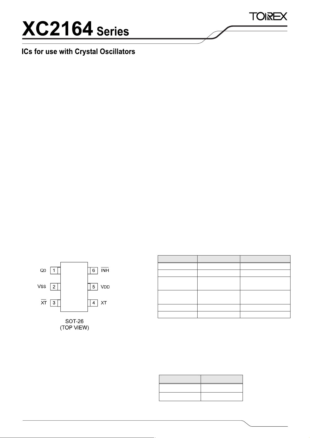
■PIN CONFIGURATION
■FEATURES
Oscillation Frequency
Divider Ratio
Output
Operating Voltage Range
Low Power Consumption
CMOS
Built-in Oscillation Feedback Resistor
Built- in Oscillation Capacitors Cg, Cd
Packages
Environmentally Friendly
■PIN ASSIGNMENT
PIN NUMBER
1 Q0 Clock Output
2 VSS Ground
3 /XT
4 XT
5 VDD Power Supply
6 /INH Stand-by Control*
*Stand-by contro l pin has a p ull-up resistor built-in. unit [μm]
: 4MHz ~ 30MHz (Fundamental)
20MHz ~ 125MHz (3rd Overtone)
: Selectable from f0/1, f0/2, f0/4,
f0/8 (f0/2, f0/4, f0/8 are
fundamental only)
: 3-State
: 3.3V
±10%, 5.0V±10%
: Stand-by function included
Selectable from Chip Enable type
and Output Enable type
: SOT-26, Chip Form (1.3x0.8mm)
: EU RoHS Compliant, Pb Free
PIN NAME FUNCTION
Crystal Oscillator
Connection (Output)
Crystal Oscillator
Connection (Input)
■
INH, Q0PIN FUNCTION
/INH Q0
“H” or OPEN Clock Output
“L” High impedance
H = High level
L = Lowlevel
1/12
r
XC2164 Series
■PAD LAYOUT FOR CHIP FORM
1.3×0.8mm
XC2164xx1xxT : 280±20μm
XC2164xx1xxF : 200±20μm
V
Level
DD
100×100μm
■PAD DIMENSIONS
PIN NUMBER
PIN
NAME
1 Q0 514 - 264
2 VSS 222 - 264
3 / XT - 450 - 264
4 XT - 450 264
5 VDD 514 27
6 / INH 47 264
PAD DIMENSIONS
X Y
■ PRODUCT CLASSIFICATION
●Ordering Information
XC2164 ①②③④⑤⑥-⑦
(*1)
DESIGNATOR DESCRIPTION SYMBOL DESCRIPTION
A Chip Enable: f0/1
B Chip Enable: f0/2 (Fundamental only)
C Chip Enable: f0/4 (Fundamental only)
①
Divider Ratio
&
/INH Pin Function
D Chip Enable: f0/8 (Fundamental only)
K Output Enable: f0/1
L Output Enable: f0/2 (Fundamental only)
M Output Enable: f0/4 (Fundamental only)
N Output Enable: f0/8 (Fundamental only)
② Chip Surface Treatment
5 Not polyimide coating on the chip surface (SOT-26 only)
6 Polyimide coating on th e chip surface (Chip form only)
③ Duty Level 1 CMOS (VDD/2) *TTL: Fundamental 4MHz to 30MHz
④
Frequency Range & Rf,
Cg, Cd Values
(Table 1) 3rd Overtone, built-in type
(Table 2) Fundamental, built-in type
MR SOT-26
⑤⑥-⑦
Packages
Taping Type
(*2)
MR-G
SOT-26
CT Chip tray (Wafer thickness : 280±20μm)
CF Chip tray (Wafer thickness : 200±20μm)
(*1)
The “-G” suffix indicates that the products are Halogen and Antimony free as well as being fully RoHS compliant.
(*2)
The device orientation is fixed in its embossed tape pocket. For reverse orientation, please contact your local Torex sales office o
representative. (Standard orientation: ⑤R-⑦, Reverse orientation: ⑤L-⑦)
Table 1: 3rd Overtone, Built-In Type
SYMBOL
FREQUENCY RANGE
3.3V ±10% 5.0V ±10%
Rf
(kΩ)
Cg
(pF)
A - 20MHz to 30MHz 9.0 21.5 21.5
B 20MHz to 30MHz 30MHz to 40MHz 6.5 20.0 20.0
C 30MHz to 40MHz 40MHz to 50MHz 5.0 16.0 16.0
D 40MHz to 50MHz 50MHz to 65MHz 3.5 14.0 14.0
E 50MHz to 65MHz 65MHz to 80MHz 2.8 12.5 12.5
F 65MHz to 80MHz 80MHz to 95MHz 2.5 10.0 10.0
H 80MHz to 95MHz 95MHz to 110MHz 2.2 8.0 8.0
K 95MHz to 110MHz 110MHz to 125MHz 2.0 7.0 7.0
L 110MHz to 125MHz - 2.3 5.5 5.5
Table 2: Fundamental, Built-In Type
SYMBOL
FREQUENCY RANGE
3.3V ±10% 5.0V ±10%
Rf
(kΩ)
Cg
(pF)
M, V 4MHz to 30MHz 4MHz to 30MHz 3.5/7.0 20.0 20.0
T 4MHz to 30MHz 4MHz to 30MHz 3.5/7.0 35.0 35.0
(*)Rf = 3.5MΩ@VDD = 5.0V Operation
Rf = 7.0 MΩ@V
=3.3V Operation
DD
2/12
unit [μm]
Cd
(pF)
Cd
(pF)
A
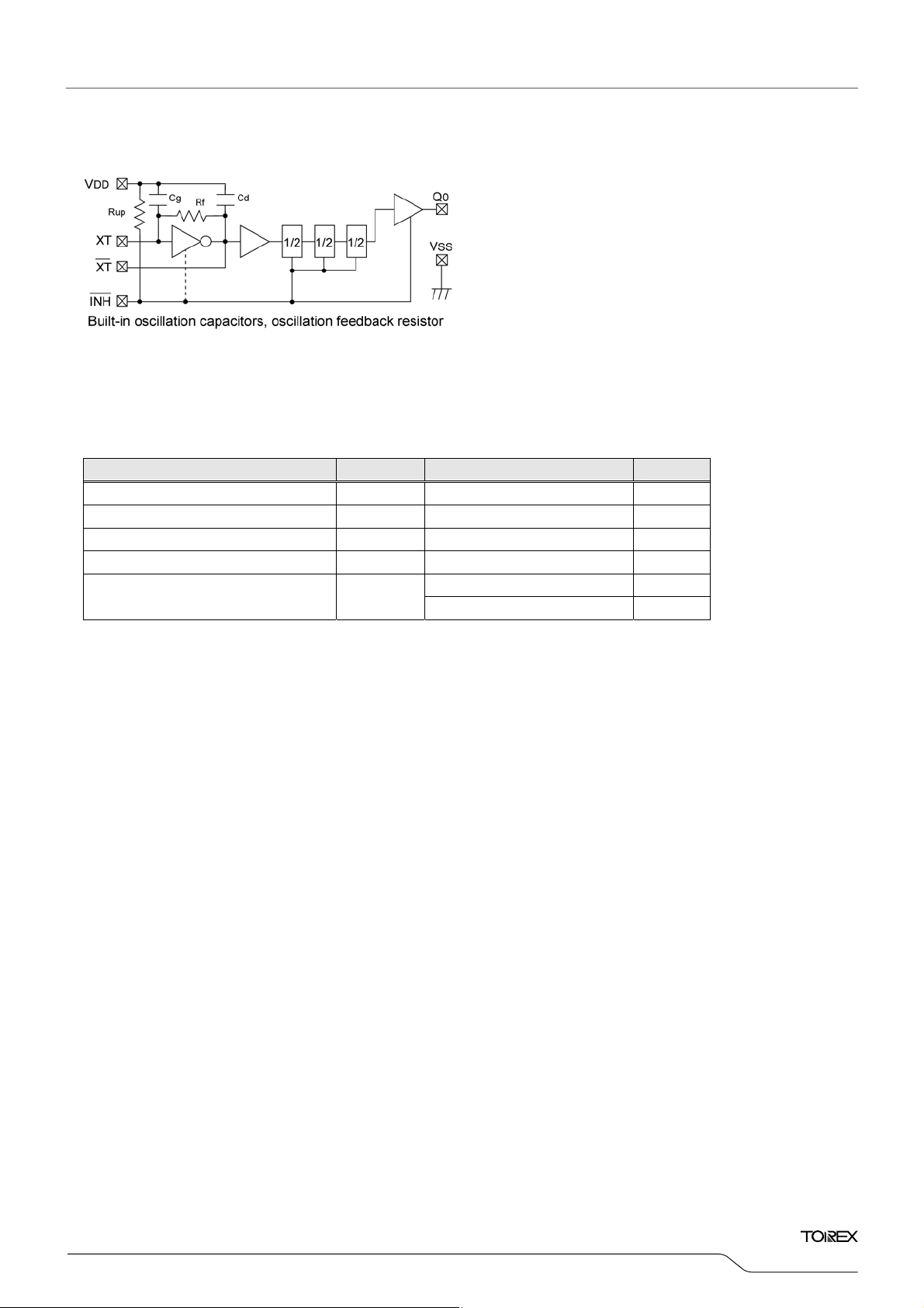
■BLOCK DIAGRAM
BSOLUTE MAXIMUM RATINGS
■
PARAMETER SYMBOL CONDITIONS UNITS
Supply Voltage VDD VSS - 0.3 ~ VSS + 7.0 V
Input Voltage VIN V
Power Dissipation Pd 250* mW
Operating Temperature Range Topr - 40 ~ + 85
Storage Temperature Range Tstg
Ta=25℃
- 0.3 ~ VDD + 0.3 V
SS
℃
- 65 ~ + 150 (Chip Form)
- 55 ~ + 125 (SOT-26)
** When implemented on a glass epoxy PCB. (SOT-26 package)
℃
℃
XC2164
Series
3/12
)
XC2164 Series
■ELECTRICAL CHARACTERISTICS
●DC Electrical Characteristics
XC2164Ax1M, T, V / XC2164Kx1M, T, V (Fundamental)
PARAMETER SYMBOL CONDITIONS MIN. TYP. MAX. UNITS
Operating Voltage VDD 4.5 5.0 5.5 V
"H" Level Input Voltage VIH 2.4 - - V
"L" Level Input Voltage VIL - - 0.4 V
"H" Level Output Voltage VOH CMOS: VDD=4.5V, IOH= - 16mA 3.9 4.2 - V
"L" Level Output Voltage VOL CMOS: VDD=4.5V, IOH=16mA - 0.3 0.4 V
Supply Current 1 I
Supply Current 2 I
Input Pull-Up Resistance 1 R
Input Pull-Up Resistance 2 R
Internal Oscillation
Feedback Resistance
Output Disable
Leak Current
* T.B.D.: T o be determined
XC2164Ax1M, XC2164Kx1M (Fundamental)
DD1
DD2
/INH="L" 0.5 1.0 2.0
UP1
/INH=0.7 VDD 25 50 100
UP2
Rf - 3.5 -
IOZ /INH="L" - - 10
PARAMETER SYMBOL CONDITIONS MIN. TYP. MAX. UNITS
Operating Voltage VDD 2.97 3.30 3.63 V
"H" Level Input Voltage VIH 2.4 - - V
"L" Level Input Voltage VIL - - 0.4 V
"H" Level Output Voltage VOH CMOS: VDD=2.97V, IOH= - 8mA 2.5 - - V
"L" Level Output Voltage VOL CMOS: VDD=2.97V, IOH=8mA - - 0.4 V
Supply Current 1 I
Supply Current 2 I
Input Pull-Up Resistance 1 R
Input Pull-Up Resistance 2 R
Internal Oscillation
Feedback Resistance
Output Disable
Leak Current
* T.B.D.: T o be determined
DD1
DD2
UP1
UP2
Q
Q
/INH="L" 1.0 2.0 4.0
/INH=0.7 VDD 35 70 140
Rf - 7.0 -
Id /INH="L" - - 10
5.0V operation (unless otherwise stated, VDD=5.0V, No Load, Ta= -30~+80℃)
/INH=Open,
Q
=Open
0
f=30MHz
/INH="L",
Q0=Open
f=30MHz
3.3V operation (unless otherwise stated, VDD=3.3V, No Load, Ta= -30~+80℃
/INH=Open,
=Open, f=30MHz
0
/INH="L",
=Open, f=30MHz
0
XC2164Ax1M, V
XC2164Ax1T
XC2164Kx1M, V
XC2164Kx1T
XC2164Ax1M, V
XC2164Ax1T
XC2164Kx1M, V
XC2164Kx1T
XC2164Ax1M - 5 (8)
XC2164Kx1M XC2164Ax1M - 2 (4)
XC2164Kx1M -
- 11 (15)
- 11 (15)
- 11 (15)
- 11 (15)
- 5 (8)
- 5 (8)
-
(T.B.D.*) (T.B.D.*)
-
9 (14)
5
(8)
(T.B.D.*) (T.B.D.*)
mA
μA
mA
MΩ
kΩ
MΩ
μA
mA
μA
mA
MΩ
kΩ
MΩ
μA
4/12

)
XC2164
Series
■ ELECTRICAL CHARACTERISTICS (Continued)
●DC Electrical Characteristics (Continued)
XC2164Ax1T, V / XC2164Kx1T, V (Fundamental)
PARAMETER SYMBOL CONDITIONS MIN. TYP. MAX. UNITS
Operating Voltage VDD 2.50 3.30 3.63 V
"H" Level Input Voltage VIH 2.4 - - V
"L" Level Input Voltage VIL - - 0.4 V
"H" Level Output Voltage VOH CMOS: 2.97V, IOH= - 8mA 2.5 - - V
"L" Level Output Voltage VOL CMOS: 2.97V, IOH=8mA - - 0.4 V
Supply Current 1 I
Supply Current 2 I
Input Pull-Up Resistance 1 R
Input Pull-Up Resistance 2 R
Internal Oscillation
Feedback Resistance
Output Disable
Leakage Current
* T.B.D.: T o be determined
Comparative Chart of Oscillation Frequency vs. Supply Voltage, and Negative Resistance Value
SYMBOL
OSCILLA TION FREQUENCY vs. SUPPL Y VOL TAGE NEGATIVE RESISTANCE VALUE
VDD=3.3V±10% VDD=5.0V±10% VDD=3.3V VDD=5.0V
DD1
DD2
/INH="L" 1.0 2.0 4.0
UP1
/INH=0.7 VDD 35 70 140
UP2
Rf - 7.0 -
IOZ /INH="L" - - 10
M ±4.3ppm ±4.5ppm
V ±1.2ppm ±2.1ppm
T ±9.4ppm ±7.0ppm
3.3V operation (unless otherwise stated, VDD=3.3V, No Load, Ta= -30~+80℃
/INH=Open,
Q0=Open,
f=30MHz
/INH="L",
Q0=Open,
f=30MHz
XC2164Ax1T
XC2164Ax1V
XC2164Kx1T
XC2164Kx1V
XC2164Ax1T
XC2164Ax1V
XC2164Kx1T
XC2164Kx1V
- 4 (6.5)
- 5 (8)
- 4 (6.5)
- 5 (8)
- 2 (4)
- 2 (4)
-
(T.B.D.*) (T.B.D.*)
-
(T.B.D.*) (T.B.D.*)
- 130Ω - 220Ω
- 150Ω - 250Ω
- 660Ω - 760Ω
(The designed value when 30MHz crystal is used.)
mA
μA
mA
MΩ
kΩ
MΩ
μA
5/12

p
)
XC2164 Series
■ ELECTRICAL CHARACTERISTICS (Continued)
●DC Electrical Characteristics (Continued)
XC2164Ax1A ~ XC2164Ax1K (3rd Overtone)
PARAMETER SYMBOL CONDITIONS MIN. TYP. MAX. UNITS
Operating Voltage VDD 4.5 5.0 5.5 V
"H" Level Input Voltage VIH 2.4 - - V
"L" Level Input Voltage VIL - - 0.4 V
"H" Level Output Voltage VOH CMOS: 4.5V, IOH= -16mA 3.9 4.2 - V
"L" Level Output Voltage VOL CMOS: 4.5V, IOH=16mA - 0.3 0.4 V
Supply Current 1 I
Supply Current 2 I
Input Pull-Up Resistance 1 R
Input Pull-Up Resistance 2 R
Internal Oscillation
Feedback Resistance
Output Disable
Leak Current
DD1
/INH="L", Q0=Open - 5.0 ( 8 )
DD2
/INH="L" 0.5 1.0 2.0
UP1
/INH=0.7 VDD 25 50 100
UP2
Rf
IOZ /INH="L" - - 10
5.0V O
/INH=Open,
=Open
Q
0
eration (Unless otherwise stated, VDD=5.0V, No Load, Ta= -30~+80℃
XC2164Ax1A, f0=30MHz - 17.0 (23)
XC2164Ax1B, f0=40MHz - 17.0 (23)
XC2164Ax1C, f0=55MHz - 19.0 (26)
XC2164Ax1D, f0=70MHz - 23.0 (32)
XC2164Ax1E, f0=85MHz - 24.0 (32)
mA
XC2164Ax1F, f0=100MHz - 30.0 (40)
XC2164Ax1H, f0=110MHz - 30.0 (40)
XC2164Ax1K, f0=125MHz - 30.0 (40)
μA
MΩ
kΩ
XC2164Ax1A - 9.0 XC2164Ax1B - 6.5 XC2164Ax1C - 5.0 XC2164Ax1D - 3.5 XC2164Ax1E - 2.8 -
kΩ
XC2164Ax1F - 2.5 -
XC2164Ax1H - 2.2 XC2164Ax1K - 2.0 -
μA
6/12

p
)
XC2164
Series
■ ELECTRICAL CHARACTERISTICS (Continued)
●DC Electrical Characteristics (Continued)
XC2164Ax1B, C, E, F, H, K, L (3rd Overtone)
PARAMETER SYMBOL CONDITIONS MIN. TYP. MAX. UNITS
Operating Voltage VDD 2.97 3.30 3.63 V
"H" Level Input Voltage VIH 2.4 - - V
"L" Level Input Voltage VIL - - 0.4 V
"H" Level Output Voltage VOH CMOS: 2.97V, IOH= - 8mA 2.5 - - V
"L" Level Output Voltage VOL CMOS: 2.97V, IOH=8mA - - 0.4 V
Supply Current 1 I
Supply Current 2 I
Input Pull-Up Resistance 1 R
Input Pull-Up Resistance 2 R
Internal Oscillation
Feedback Resistance
Output Disable
Leak Current
XC2164Ax1D (3rd Overtone)
DD1
DD2
UP1
UP2
Rf
IOZ /INH="L" - - 10
3.3V Operation (Unless otherwise stated, VDD=3.3V, Oscillation Frequency f0=48MHz, Ta= -30~+80℃)
/INH=Open,
Q0=Open
/INH="L", Q0=Open - 2.0 -
/INH="L" 1.0 2.0 4.0
/INH=0.7 VDD 35 70 140
PARAMETER SYMBOL CONDITIONS MIN. TYP. MAX. UNITS
Operating Voltage VDD 2.70 3.30 3.63 V
'H' Level Input Voltage VIH
'L' Level Input Voltage VIL
'H' Level Output Voltage VOH
'L' Level Output Voltage VOL CMOS: 2.97V, IOH=8mA - - 0.4 V
Supply Current 1 I
Supply Current 2 I
Input Pull-Up Resistance 1 R
Input Pull-Up Resistance 2 R
Internal Oscillation
Feedback Resistance
Output Disable Leak
Current
DD1
DD2
Rf
I
OZ
UP1
UP2
/INH=Open,
Q
=Open
0
eration (unless otherwise stated, VDD=3.3V, No Load, Ta= -30~+80℃
3.3V O
XC2164Ax1B, f0=30MHz - 4.5 (7)
XC2164Ax1C, f0=40MHz - 5.0 (8)
XC2164Ax1E, f0=70MHz - 8.0 (13)
XC2164Ax1F, f0=85MHz - 8.5 (13)
XC2164Ax1H, f0=100MHz - 9.5 (15)
XC2164Ax1K, f0=110MHz - 10.0 (15)
XC2164Ax1L, f0=125MHz - 10.5 (15)
XC2164Ax1B - 6.5 XC2164Ax1C - 5.0 XC2164Ax1E - 2.8 XC2164Ax1F - 2.5 XC2164Ax1H - 2.2 XC2164Ax1K - 2.0 XC2164Ax1L - 2.3 -
CMOS: 2.97V, I
OH
/INH = 'L', Q0=Open
/INH = 'L'
/INH = 0.7V
XC2164Ax1D
/INH = 'L'
= - 8mA
XC2164Ax1D,
f0=55MHz
DD
2.4 - - V
- - 0.4 V
2.5 - - V
- 6.5 (10) mA
- 2.0 -
1.0 2.0 4.0
35 70 140
- 3.5 -
- - 10
mA
μA
MΩ
kΩ
kΩ
μA
μA
MΩ
kΩ
kΩ
μA
7/12

XC2164 Series
■SWITCHING CHARACTERISTICS
XC2164Ax1M, T, V (Fundamental) <Chip Enable> (unless otherwise stated, VDD=3.3V or 5.0V, Ta= -30~+80℃)
PARAMETER SYMBOL CONDITIONS MIN. TYP. MAX. UNITS
Output Rise Time
Output Fall Time
(*1)
tr
(*1)
tf
Output Duty Cycle DUTY
CMOS: CL=15pF, 0.1VDD→0.9VDD
TTL: Load=10TTL, 0.4V →2.4V
CMOS: CL=15pF, 0.9VDD→0.1VDD
TTL: Load=10TTL, 2.4V →0.4V
CMOS: CL=15pF @ 0.5VDD 45 - 55 %
- 1.5 - ns
- 1.5 - ns
- 1.5 - ns
- 1.5 - ns
TTL: Load=10TTL @ 1.4V 45 - 55 %
Output Disable Delay Time
Output Enable Delay Time
Oscillation Start Time
XC2164Ax1A to L (3rd Overtone) <Chip Enable> (unless otherwise stated, VDD=3.3V or 5.0V, Ta= -30~+80℃)
(*1)
tplz f0=4MHz, CL=15pF - - 100 ns
(*1)
tplz f0=4MHz, CL=15pF - - 6 ms
(*1)
tosc_on f0=4MHz, CL=15pF - - 6 ms
*1: the values are the designed values.
PARAMETER SYMBOL CONDITIONS MIN. TYP. MAX. UNITS
Output Rise Time
Output Fall Time
(*1)
tr
(*1)
tf
Output Duty Cycle DUTY
CMOS: CL=15pF, 0.1VDD→0.9VDD
TTL: Load=10TTL, 0.4V →2.4V
CMOS: CL=15pF, 0.9VDD→0.1VDD
TTL: Load=10TTL, 2.4V →0.4V
CMOS: CL=15pF @ 0.5VDD 45 - 55 %
- 1.5 - ns
- 1.5 - ns
- 1.5 - ns
- 1.5 - ns
TTL: Load=10TTL @ 1.4V 45 - 55 %
Output Disable Delay Time
Output Enable Delay Time
Oscillation Start Time
XC2164Kx1M, T, V (Fundamental) <Output Enable>
(*1)
tplz f0=20MHz, CL=15pF - - 100 ns
(*1)
tplz f0=20MHz, CL=15pF - - 6 ms
(*1)
tosc_on f0=20MHz, CL=15pF - - 6 ms
*1: the values are the designed values.
(unless otherwise stated, VDD=3.3V or 5.0V, Ta= -30~+80℃)
PARAMETER SYMBOL CONDITIONS MIN. TYP. MAX. UNITS
Output Rise Time
(*1)
tr
CMOS: CL=15pF, 0.1VDD→0.9VDD
TTL: Load=10TTL, 0.4V →2.4V
Output Fall Time
(*1)
tf
CMOS: CL=15pF, 0.9VDD→0.1VDD
TTL: Load=10TTL, 2.4V →0.4V
Output Duty Cycle DUTY
CMOS: CL=15pF @ 0.5VDD 45 - 55 %
TTL: Load=10TTL @ 1.4V 45 - 55 %
Output Disable Delay Time
Output Enable Delay Time
Oscillation Start Time
* The values shown are preliminary so that the values may be changed without a prior announcement.
(*1)
tplz f0=4MHz, CL=15pF - - 100 ns
(*1)
tplz f0=4MHz, CL=15pF - - 10
(*1)
tosc_on f0=4MHz, CL=15pF - - 6 ms
8/12
- 1.5 - ns
- 1.5 - ns
- 1.5 - ns
- 1.5 - ns
μs
*1: the values are the designed values.

y Cy
■SWITCHING WAVEFORMS
● Switching Time
(1) CMOS Output
(2) TTL Output
● Dut
(1) CMOS Output
(2) TTL Output
cle
XC2164
Series
9/12

XC2164 Series
■SWITCHING WAVEFORMS (Continued)
(3) Output Disable Delay Time, Output Enable Delay Time *)The /INH pin input waveform: less than tr=tf=10ns, VDD input
(4) Oscillation Start Time: tosc_on *)The V
DD pin input waveform : less than tr=tf=10ns,/INH=Open
10/12

(
)
■ PACKAGING INFORMATION
●SOT-26
■ MARKING RULE
●SOT-26
654
① ② ③ ④
123
SOT-26
(TOP VIEW)
XC2164
Series
① represents product series
MARK
4
② represents divider ratio
<Chip Enable>
MARK RATIO MARK RATIO
A f0/1 C f0/4
B f0/2 D f0/8
*B, C, D: fundamental only
<Output Enable>
MARK RATIO MARK RATIO
K f0/1 M f0/4
L f0/2 N f0/8
*L, M, N: fundamental only
③ represents recommended frequency & Rf, Cg &Cd values
* Please refer to the ordering information, SYMBOL ① to ④
④ represents assembly lot number
Based on internal standards
11/12

XC2164 Series
1. The products and product specifications contained herein are subject to change without
notice to improve performance characteristics. Consult us, or our representatives
before use, to confirm that the information in this datasheet is up to date.
2. We assume no responsibility for any infringement of patents, patent rights, or other
rights arising from the use of any information and circuitry in this datasheet.
3. Please ensure suitable shipping controls (including fail-safe designs and aging
protection) are in force for equipment employing products listed in this datasheet.
4. The products in this datasheet are not developed, designed, or approved for use with
such equipment whose failure of malfunction can be reasonably expected to directly
endanger the life of, or cause significant injury to, the user.
(e.g. Atomic energy; aerospace; transport; combustion and associated safety
equipment thereof.)
5. Please use the products listed in this datasheet within the specified rang es.
Should you wish to use the products under conditions exceeding the specifications,
please consult us or our representatives.
6. We assume no responsibility for damage or loss due to abnormal use.
7. All rights reserved. No part of this datasheet may be copied or reproduced without the
prior permission of TOREX SEMICONDUCTOR LTD.
12/12
 Loading...