


■
■
A
■
■
/
■
XC2163 Series
ETR1403_001a
ICs for use with 3rd Overtone Crystal Oscillators
GENERAL DESCRIPTIO N
The XC2163 series are high frequency, low current consumption CMOS ICs with built-in crystal oscillator and divider circuits.
Output is selectable from any one of the following values for f0: f0/1, f0/2, f0/4, f0/8.
With oscillation capacitors and a feedback resistors built-in, it is possible to configure a stable 3rd overtone oscillator using
only an external crystal oscillator.
Also available is an external oscillation capacitor/external oscillation feedback resistor type, which makes oscillation
frequency control possible.
PPLICATIONS
●Crystal Oscillation Modules
●Computer, DSP Clocks
●Communication Equipment
●Various System Clocks
PIN CONFIGURATION
FEATURES
Oscillation Frequency : 40MHz ~ 125MHz
(Rf, Cg, Cd internal; 5.0V)
(3rd Overtone) : 57MHz ~ 125MHz
(Rf, Cg, Cd internal; 3.3V)
: 20MHz ~ 125MHz
(Rf, Cg, Cd external)
Divider Ratio : Selectable from f0/1, f0/2,
f0/4, f0/8.
Output : 3-State
Operating Voltage Range : 3.3V ±10%, 5.0V ±10%
Low Current Consumption
CMOS
Built-in Oscillation Capacitor
Built-in Oscillation Feedback Resistor
Package : SOT-26
Environmentally Friendly
* Oscillation continues in stand-by mode
: Stand-by function included *
: EU RoHS Compliant, Pb Free
■PIN ASSIGNMENT
PIN
NUMBER
1 /INH Stand-by Control*
2 XT
3 VSS GND
4 Q0 Clock Output
5 VDD Power Supply
6 /XT
* Stand-by control pin has a pull-up resistor built-in.
PIN NAME FUNCTION
Crystal Oscillator Connection
(Input)
Crystal Oscillator Connection
(Output)
INH, Q0 PIN FUNCTION
/INH "H" or OPEN "L"(Stand-by)
Q0 Divider Output High Impedance
"H" = High Level
"L" = Low Level
1/9

■
XC2163 Series
PRODUCT CLASSIFICATION
●Ordering Information
XC2163①②③④⑤⑥‑⑦
DESIGNATOR DESCRIPTION SYMBOL DESCRIPTION
①
②
③
④
⑤⑥‑⑦
(*1)
The “-G” suffix indicates that the products are Halogen and Antimony free as well as being fully RoHS compliant.
(*2)
The device orientation is fixed in its embossed tape pocket. For reverse orientation, please contact your local Torex sales office or
representative. (Standard orientation: ⑤R-⑦, Reverse orientation: ⑤L-⑦)
Table 1: Frequency for External Type
SYMBOL
Z
Note: We recommend that a damping resistor Rd be added between the /XT pin & the crystal oscillator pin in order
Table 2: Frequency for Built-In Type
SYMBOL
A - - -
B - - C
D
E
F
H
K
L
FREQUENCY RANGE Rf Cg/Cd FREQUENCY RANGE Rf Cg/Cd
108MHz〜125MHz 1.6kΩ
93MHz〜110MHz 2.4kΩ
80MHz〜95MHz 2.4kΩ
68MHz〜83MHz 2.4kΩ
55MHz〜70MHz 3.3kΩ
45MHz〜57MHz 3.3kΩ
35MHz〜47MHz 3.6kΩ
28MHz〜37MHz 4.7kΩ
24MHz〜30MHz 5.6kΩ
20MHz〜26MHz 6.8kΩ
to safeguard the crystal oscillator and improve oscillation stability.
FREQUENCY RANGE Rf Cg/Cd FREQUENCY RANGE Rf Cg/Cd
108MHz〜125MHz 2.2kΩ
95MHz〜110MHz 2.4kΩ
80MHz〜97MHz 3.2kΩ
68MHz〜83MHz 3.7kΩ
55MHz〜70MHz 4.9kΩ
45MHz〜57MHz 5.5kΩ
40MHz〜48MHz 6.5kΩ
(*1)
C : f0/1
Divider Ratio
D : f0/2
E : f0/4
F : f0/8
Output Capacity 5 : 10TTL
Duty Level 1 : CMOS (V
Frequency Range &
Rf, Cg, Cd Values
Packages
Taping Type
(*2)
Z : External type (refer to table 1)
A〜L
: Built-in type (refer to table 2)
MR-G : SOT-26
5.0V TYPE 3.3V TYPE
10pF
10pF
108MHz〜125MHz 3.9kΩ
95MHz〜110MHz 2.4kΩ
12pF
15pF
15pF
20pF
24pF
27pF
30pF
33pF
- - -
5.0V TYPE 3.3V TYPE
108MHz〜125MHz 1.5kΩ
93MHz〜110MHz 1.7kΩ
5.5pF
6.5pF
6.5pF
6.5pF
7.6pF - - -
11.0pF - - -
11.0pF - - -
DD/2) *TTL : 20MHz to 37MHz
80MHz〜97MHz 2.7kΩ
68MHz〜83MHz 2.7kΩ
58MHz〜70MHz 3.9kΩ
50MHz〜60MHz 3.9kΩ
40MHz〜52MHz 2.4kΩ
33MHz〜42MHz 3.6kΩ
28MHz〜35MHz 3.6kΩ
24MHz〜30MHz 3.9kΩ
20MHz〜26MHz 3.9kΩ
80MHz〜95MHz 2.2kΩ
72MHz〜83MHz 2.4kΩ
65MHz〜75MHz 3.2kΩ
57MHz〜67MHz 3.7kΩ
4pF
7pF
8pF
10pF
10pF
12pF
20pF
20pF
24pF
27pF
33pF
5.5pF
6.5pF
5.5pF
6.5pF
6.5pF
6.5pF
2/9

■
■
A
BLOCK DIAGRAMS
BSOLUTE MAXIMUM RATINGS
PARAMETER SYMBOL CONDITIONS UNITS
Supply Voltage VDD
Input Voltage VIN
SS-0.3〜VSS+7.0
V
SS-0.3〜VDD+0.3
V
Power Dissipation Pd 250 * mW
Operating
Temperature Range
Storage
Temperature Range
* When implemented on a glass epoxy PCB.
Topr
Tstg
-30〜+80 ℃
-55〜+125 ℃
V
V
XC2163
Series
3/9
■
■
XC2163 Series
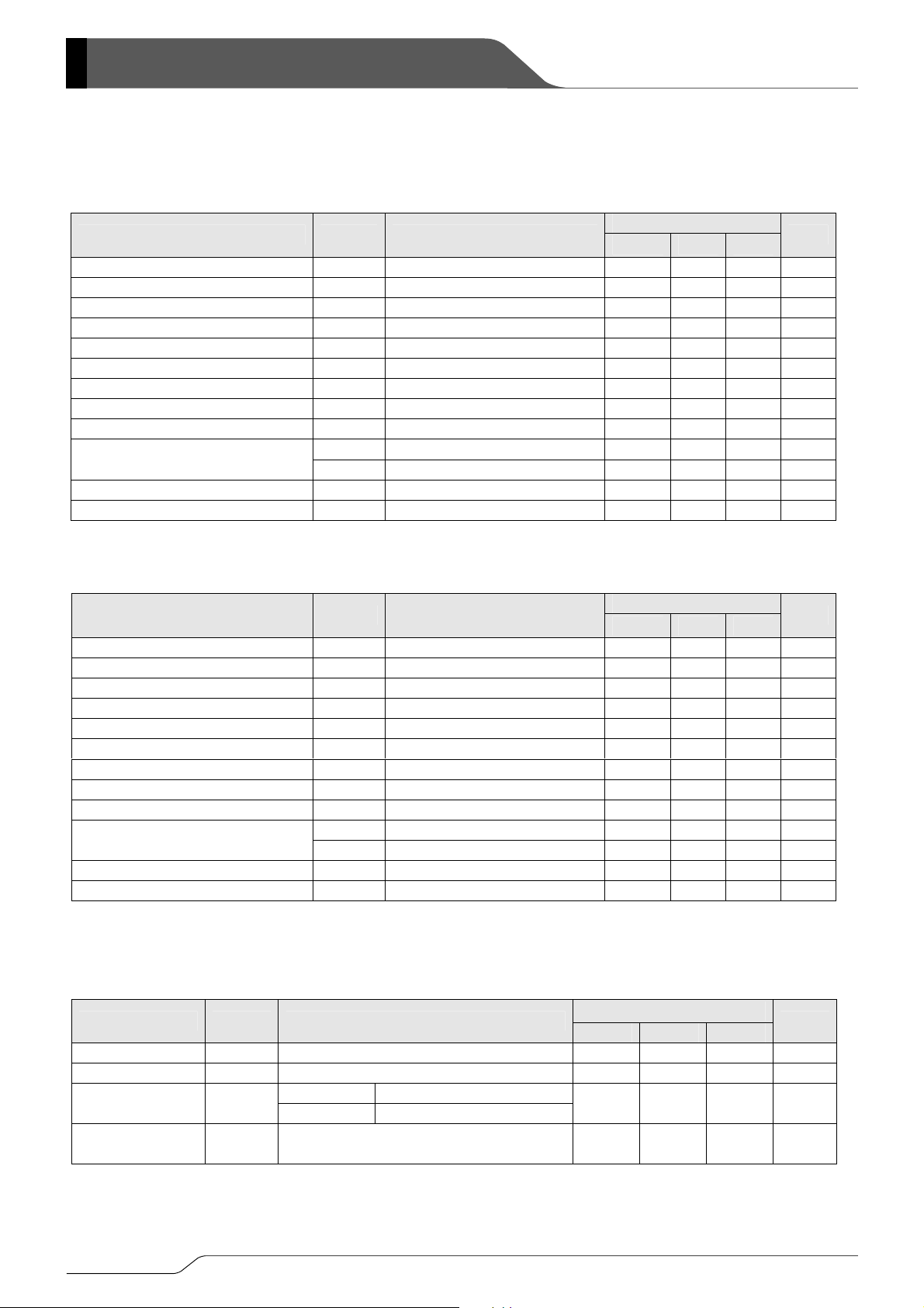
ELECTRICAL CHARACTERISTICS
XC2163C51AMR
FOSC=108MHz~125MHz
PARAMETER SYMBOL CONDITIONS
Operating Voltage VDD 2.97 - 3.63 V
'H' Level Input Voltage VIH /INH pin 2.4 - - V
'L' Level Input Voltage VIL /INH pin - 0.4 V
'H' Level Output Voltage VOH Qo pin, VDD =2.97V, IOH = 8mA 2.2 2.4 - V
'L' Level Output Voltage VOL Qo pin, VDD = 2.97V, IOL = 8mA - 0.3 0.4 V
Supply Current 1 IDD1 /INH = OPEN, CL = 15pF, f = 125MHz - 18 - mA
Supply Current 2 IDD2 /INH = 'L', f = 125MHz - 5 - mA
Input Pull-Up Resistance 1 Rup1 /INH = 'L' 1.0 2.0 4.0
Input Pull-Up Resistance 2 Rup2 /INH = 0.7VDD 35 70 140
Internal Oscillation Capacity
Internal Oscillation Feedback Resistance Rf - 1.5 -
Output Off Leak Current IOZ Qo pin, /INH = 'L' - - 10
XC2163C51BMR
FOSC=93MHz~110MHz
PARAMETER SYMBOL CONDITIONS
Operating Voltage VDD 2.97 - 3.63 V
'H' Level Input Voltage VIH /INH pin 2.4 - - V
'L' Level Input Voltage VIL /INH pin - - 0.4 V
'H' Level Output Voltage VOH Qo pin, VDD = 2.97V, IOH = 8mA 2.2 2.4 - V
'L' Level Output Voltage VOL Qo pin, VDD = 2.97V, IOL = 8mA - 0.3 0.4 V
Supply Current 1 IDD1 /INH = OPEN, CL = 15pF, f = 110MHz - 15 - mA
Supply Current 2 IDD2 /INH = 'L', f = 110MHz - 5 - mA
Input Pull-Up Resistance 1 Rup1 /INH = 'L' 1.0 2.0 4.0
Input Pull-Up Resistance 2 Rup2 /INH = 0.7VDD 35 70 140
Internal Oscillation Capacity
Internal Oscillation Feedback Resistance Rf - 1.7 -
Output Off Leak Current IOZ Qo pin, /INH = 'L' - - 10
SWITCHING CHARACTERISTICS
XC2163C51AMR/XC2163C51BMR
PARAMETER SYMBOL CONDITIONS
Output Rise Time tr
Output Fall Time tf
Output Duty Cycle DUTY
Output Disable
Delay Time
tplz C
Cg R&D Value - 5.5 - pF
Cd R&D Value - 5.5 - pF
(Unless otherwise stated, V
Cg R&D Value - 6.5 - pF
Cd R&D Value - 6.5 - pF
C
L=15pF, 0.1VDD→0.9VDD
C
L=15pF, 0.9VDD→0.1VDD
C51A 0.5VDD, CL=15pF, f=125MHz
C51B 0.5V
DD, CL=15pF, f=110MHz
L=15pF - - 100 ns
(Unless otherwise stated, V
STANDARD VALUE
MIN. TYP. MAX.
DD=3.3V, No load, Ta=25℃)
STANDARD VALUE
MIN. TYP. MAX.
CMOS DUTY:V
STANDARD VALUE
MIN. TYP. MAX.
- 1.5 - ns
- 1.5 - ns
45 - 55 %
DD=3.3V , Ta=25℃)
UNITS
MΩ
kΩ
kΩ
μA
Note) R&G value
UNITS
MΩ
kΩ
kΩ
μA
DD=3.3V , Ta=25℃
UNITS
4/9
■
■
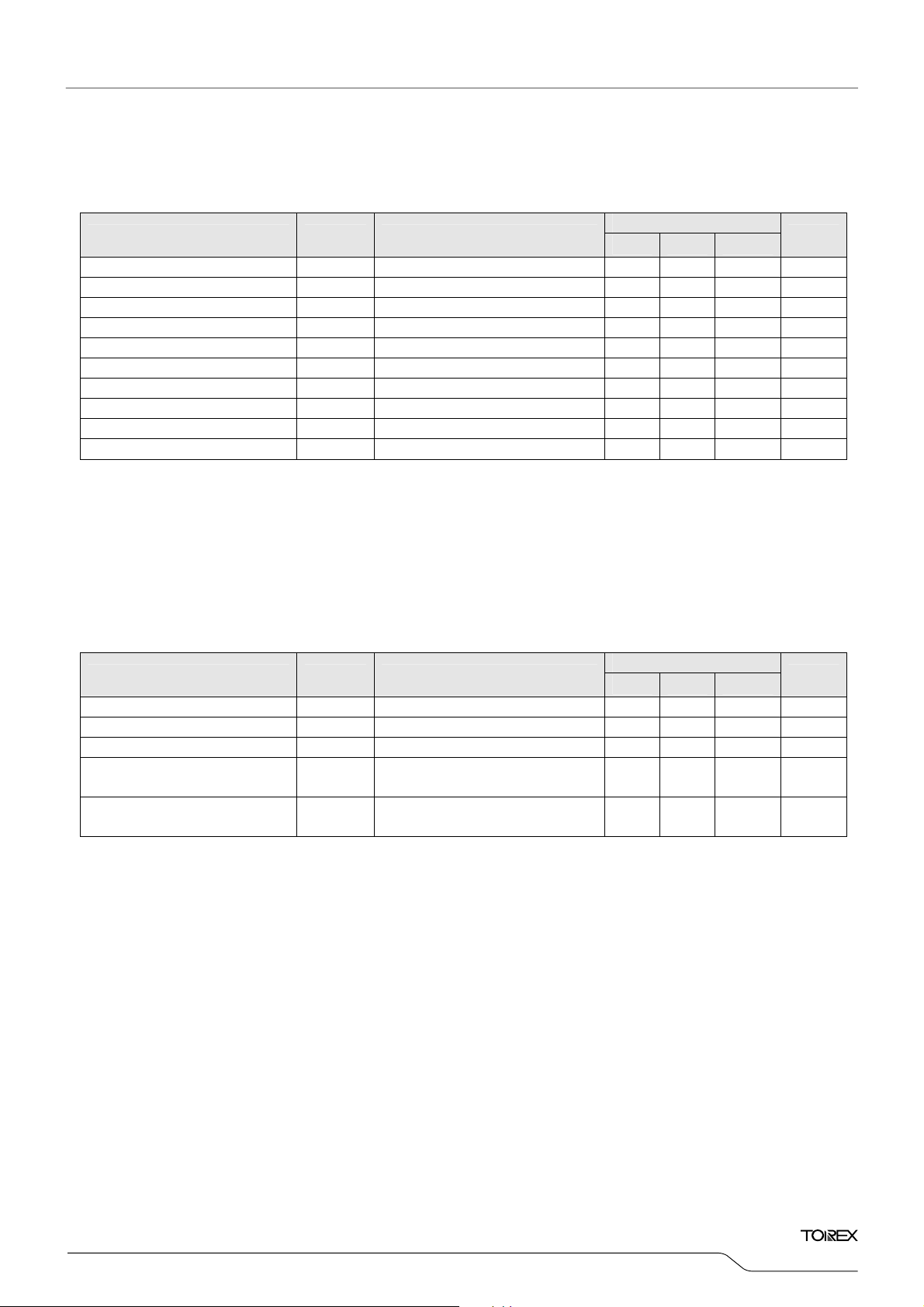
ELECTRICAL CHARACTERISTICS (Continued)
XC2163C51ZMR
FOSC = 108MHz to 125MHz; Rf = 1.6kΩ, Cg = Cd = 10pF external
PARAMETER SYMBOL CONDITIONS
Operating Voltage VDD 4.5 - 5.5 V
'H' Level Input Voltage VIH /INH pin 2.4 - - V
'L' Level Input Voltage VIL /INH pin - - 0.4 V
'H' Level Output Voltage VOH Qo pin, VDD = 4.5V, IOH = -16mA 3.9 4.2 - V
'L' Level Output Voltage VOL Qo pin, VDD = 4.5V, IOL = 16mA - 0.3 0.4 V
Supply Current 1 IDD1 /INH = OPEN, CL = 15pF, f = 120MHz - 31 - mA
Supply Current 2 IDD2 /INH = 'L', f = 120MHz - 14 - mA
Input Pull-Up Resistance 1 Rup1 /INH = 'L' 0.5 1.0 2.0
Input Pull-Up Resistance 2 Rup2 /INH = 0.7VDD 25 50 100
Output Off Leak Current IOZ Qo pin, /INH = 'L' - - 10
SWITCHING CHARACTERISTICS
XC2163C51ZMR
PARAMETER SYMBOL CONDITIONS
Output Rise Time tr
Output Fall Time tf
Output Duty Cycle DUTY 0.5VDD, CL=15pF, f=120MHz 45 - 55 %
Output Disable
Delay Time
Output Enable
Delay Time
tplz C
tpzl C
C
L=15pF, 0.1VDD→0.9VDD
C
L=15pF, 0.9VDD→0.1VDD
L=15pF - - 100 ns
L=15pF - - 100 ns
XC2163
Series
(Unless otherwise stated, V
STANDARD VALUE
MIN. TYP. MAX.
CMOS DUTY : V
STANDARD VALUE
MIN. TYP. MAX.
- 1.5 - ns
- 1.5 - ns
The contents can be changed without advance notice.
DD=5.0V , Ta=25℃)
UNITS
MΩ
kΩ
μA
DD=5.0V , Ta=25℃
UNITS
5/9
■
■
XC2163 Series
ELECTRICAL CHARACTERISTICS (Continued)
XC2163C51ZMR
FOSC= 108MHz to 125MHz : Rf = 3.9kΩ, Cg = Cd = 4pF external
PARAMETER SYMBOL CONDITIONS
Operating Voltage VDD 2.97 - 3.63 V
'H' Level Input Voltage VIH /INH pin 2.4 - - V
'L' Level Input Voltage VIL /INH pin - - 0.4 V
'H' Level Output Voltage VOH Qo pin, VDD = 2.97V, IOH = -8mA 2.2 2.4 - V
'L' Level Output Voltage VOL Qo pin, VDD = 2.97V, IOL = 8mA - 0.3 0.4 V
Supply Current 1 IDD1 /INH = OPEN, CL = 15pF, f = 120MHz - 15 - mA
Supply Current 2 IDD2 /INH = 'L', f = 100MHz - 4 - mA
Input Pull-Up Resistance 1 Rup1 /INH = 'L' 2.0 4.0 6.0
Input Pull-Up Resistance 2 Rup2 /INH = 0.7VDD 70 140 250
Output Off Leak Current IOZ Qo pin, /INH = 'L' - - 10
SWITCHING CHARACTERISTICS
XC2163C51ZMR
PARAMETER SYMBOL CONDITIONS
Output Rise Time tr CL=15pF, 0.1VDD ~ 0.9VDD - 1.5 - ns
Output Fall Time tf CL=15pF, 0.9VDD ~ 0.1VDD - 1.5 - ns
Output Duty Cycle DUTY 0.5VDD, CL=15pF, f=120MHz 45 - 55 %
Output Disable
Delay Time
Output Enable
Delay Time
tplz C
tpzl C
L=15pF - - 100 ns
L=15pF - - 100 ns
(Unless otherwise stated, V
STANDARD VALUE
MIN. TYP. MAX.
CMOS DUTY : V
STANDARD VALUE
MIN. TYP. MAX.
The contents can be changed without advance notice.
DD=3.3V , Ta=25℃)
UNITS
MΩ
kΩ
μA
DD=3.3V , Ta=25℃
UNITS
6/9
■
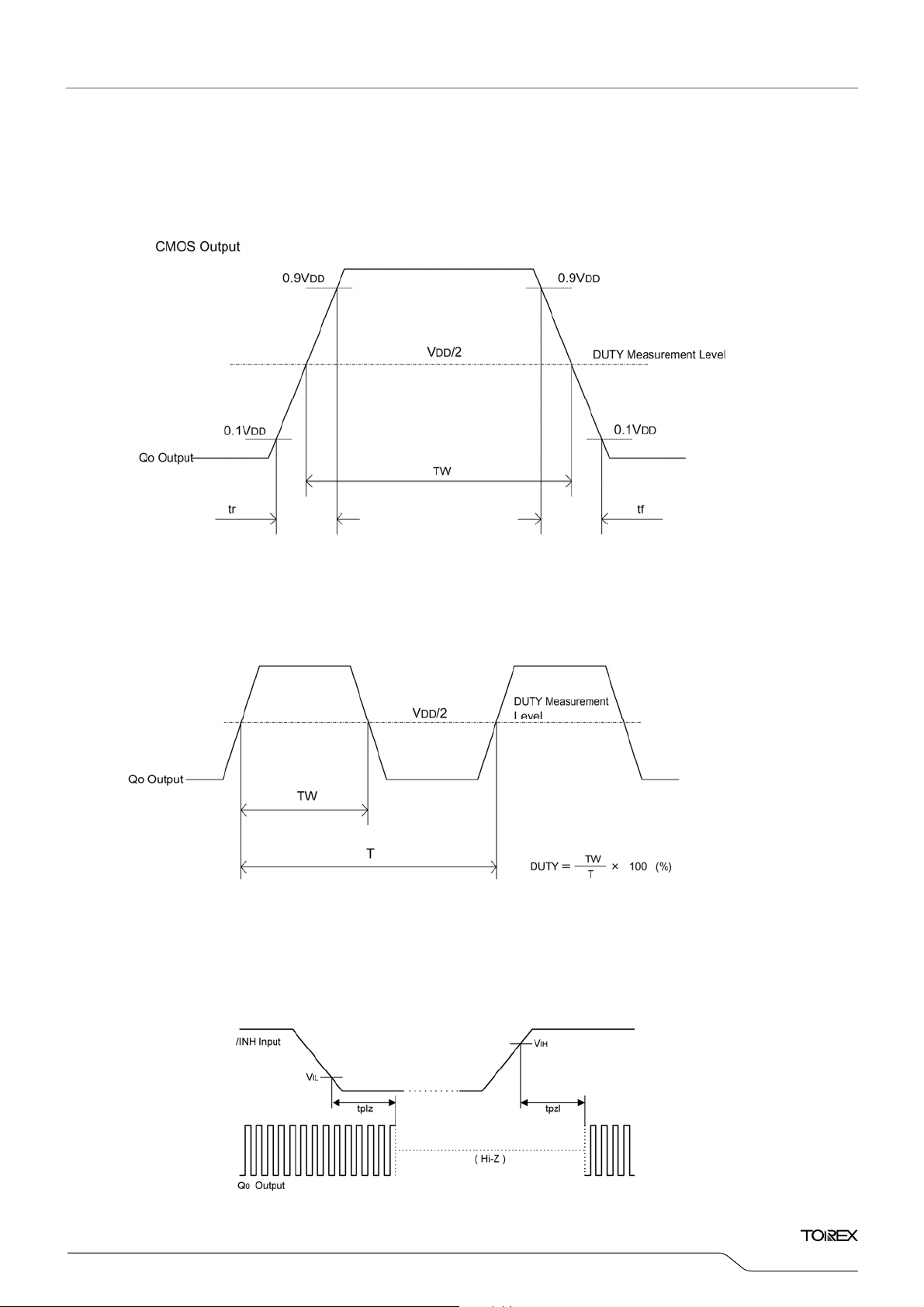
SWITCHING CHARACTERISTICS MEASUREMENT WAVEFORMS
(1) Switching Time
(2) Output Waveform Symmetry
(3) Output Disable Delay Time, Output Enable Delay Time
NH Pin Input Waveform tr = tf = less than 10ns
*) /I
XC2163
Series
7/9

■
■
XC2163 Series
PACKAGING INFORMATION
●SOT-26
MARKING RULE
SOT-26
(TOP VIEW)
①Represents product series
MARK
6
②Represents divider ratio
MARK RATIO MARK RATIO
C fo/1 E fo/4
D fo/2 F fo/8
③Represents frequency & Rf,
Cg & Cd values
MARK
Frequency (MHz)
5.0V 3.3V
A - 108~125
B - 93~110
C 108~125 80~95
D 95~110 72~83
E 80~97 65~75
F 68~83 57~67
H 55~70 K 45~57 L 40~48 Z External
④Represents assembly lot number
(Based on internal standards)
8/9
XC2163
Series
1. The products and product specifications contained he rein are subject to change without
notice to improve performance characteristics. Consult us, or our representatives
before use, to confirm that the information in this datasheet is up to date.
2. We assume no responsibility for any infringement of patents, patent rights, or other
rights arising from the use of any information and circuitry in this datasheet.
3. Please ensure suitable shipping controls (including fail-safe designs and aging
protection) are in force for equipment employing products listed in this datasheet.
4. The products in this datasheet are not developed, designed, or approved for use with
such equipment whose failure of malfunction can be reasonably expected to directly
endanger the life of, or cause significant injury to, the user.
(e.g. Atomic energy; aerospace; transport; combustion and associated safety
equipment thereof.)
5. Please use the products listed in this datasheet within the specified ranges.
Should you wish to use the products under conditions exceeding the specifications,
please consult us or our representatives.
6. We assume no responsibility for damage or loss due to abnormal use.
7. All rights reserved. No part of this datasheet may be copied or reproduced without the
prior permission of TOREX SEMICONDUCTOR LTD.
9/9
 Loading...