


■
■
A
■
■
■
XC2141 Series
ETR1401_001a
ICs for use with Crystal Oscillators
GENERAL DESCRIPTIO N
The XC2141 series are a group of high frequency, CMOS low power crystal oscillators with on-chip divider circuitry that
operate from a supply voltage of 3.5V.
PPLICATIONS
●Crystal oscillator modules
●Communication equipment
●Microcomputers
●Clock units in motor control
●System clocks on boards
●Timers
●Palmtops
PIN CONFIGURATION
INH, Q0 PIN FUNCTION
/INH Q0
"H" Output
open Output
"L" High Impedance (oscillation stopped)
"H" = High level
"L" = Low level
SOT-26
(TOP VIEW)
FEATURES
Oscillation Frequency : 20MHz ~ 58MHz
Divider Ratio : f0/1
Output : 3-State
Operating Voltage Range : 3.5V ±10%
Small Quiescent Current : 10mA (F
Stand-By Funct
CMOS : Low Power Consumption
Ultra Small Package : SOT-26 (150mW)
Environmentally Friendly : EU RoHS Compliant, Pb Free
OSC=53MHz)
■PIN ASSIGNMENT
PIN
NUMBER
1 /INH Control *
2 XT Oscillator Connection (Input)
3 VSS GND
4 Q0 Output
5 VDD Power Supply
6 /XT Oscillator Connection (Output)
* Control pin has pull-up resistor built-in.
PIN NAME FUNCTION
1/6
■
■
r
XC2141 Series
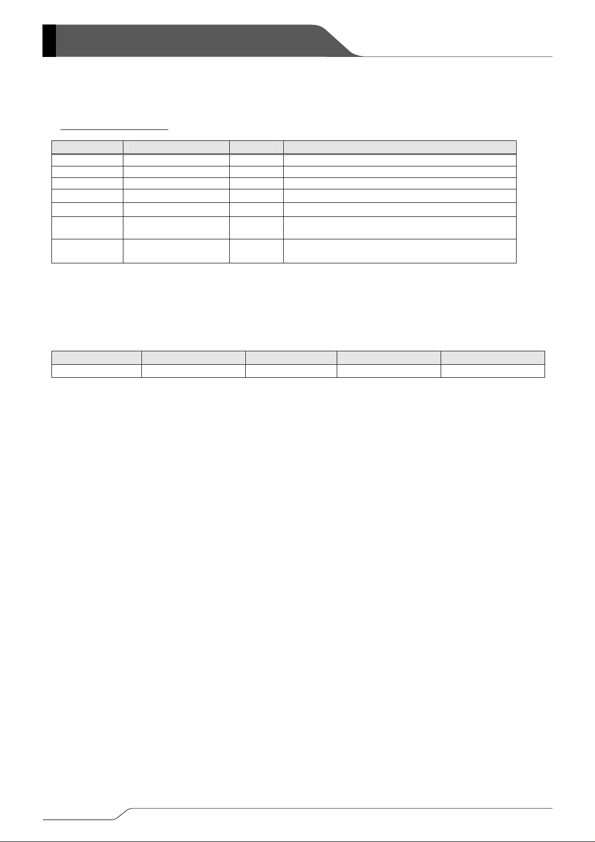
PRODUCT CLASSIFICATION
●Ordering Information
XC21①②③④⑤⑥⑦⑧‑⑨
DESIGNATOR DESCRIPTION SYMBOL DESCRIPTION
① Supply Voltage 4 : 3.5V
② Product Series 1 : Large output capability, fundamental & overtone
③ Duty Level C : CMOS (VDD/2)
④ Fixed Number 2 : Fixed
⑤ Divider Ratio 1 : f0/1
⑥
Fundamental / Overtone
⑦⑧-⑨
(*1)
The “-G” suffix indicates that the products are Halogen and Antimony free as well as being fully RoHS compliant.
(*2)
The device orientation is fixed in its embossed tape pocket. For reverse orientation, please contact your local Torex sales office o
representative. (Standard orientation: ⑦R-⑨, Reverse orientation: ⑦L-⑨)
STANDARD PARTS
PART NUMBER DUTY LEVEL DIVIDER Rf Cg & Cd
XC2141C21A CMOS (VDD/2) f0/1 External External
Cg & Cd: Add a 2pF capacitor between VDD & XT and/or VDD & XT/. As the parasitic capacitance, Cg and Cd's capacitance is equivalent of
2pF.
(*1)
Rf, Cg, Dc
Packages
Taping Type
(*2)
A : No Rf, Cg, Cd = 2pF
MR-G : SOT-26
2/6

■
■
A
■
BLOCK DIAGRAM
BSOLUTE MAXIMUM RATINGS
XC2141
Series
PARAMETER SYMBOL CONDITIONS UNITS
Supply Voltage VDD VSS - 0.3 ~ VSS + 7.0 V
Input Voltage VIN VSS - 0.3 ~ VDD + 0.3 V
Power Dissipation Pd 150 mW
Operating Temperature Range Topr -30 ~ +75
Storage Temperature Range Tstg -55 ~ +125
ELECTRICAL CHARACTERISTICS
XC2141C21AMR (Overtone) f0/1
VDD=3.5V, FOSC=53MHz, Rf=7.5kΩ, No Load, Ta = 25℃
PARAMETER SYMBOL CONDITIONS MIN. TYP. MAX. UNITS
Operating Supply Voltage VDD 3.15 3.50 3.85 V
Oscillation Start-Up Time TST
Input Voltage 'High' VIH 2.4
Input Voltage 'Low' VIL
Output Current 'High' IOH VOH = 3.15V
Output Current 'Low' IOL VOL = 0.35V
Supply Current 1 IDD1 / INH = OPEN, Q0 = OPEN
Supply Current 2 IDD2 / INH = "L"
Input Pull-Up Resistance RUP / INH = 3.15V 50
Output Disable Leak Current IOZ / INH = "L"
−
− −
−
−
− −
− −
− −
5.00
− −
- 8
12
−
℃
℃
−
0.4 V
−
−
10 mA
520
200
10
ms
V
mA
mA
μA
kΩ
μA
3/6

■
XC2141 Series
SWITCHING CHARACTERISTICS
CMOS Duty, VDD=3.5V, Load = 15pF, Ta = 25℃
PARAMETER SYMBOL CONDITIONS MIN. TYP. MAX. UNITS
Output Rise Time TTLH 0.1VDD 0.9VDD - - 9 ns
Output Fall Time TTHL 0.9VDD 0.1VDD - - 8 ns
Duty Cycle 1 DUTY 1 at VDD/2, f0/1 Output 40 - 60 %
4/6

■
■
PACKAGING INFORMATION
●SOT-26
MARKING RULE
XC2141
Series
①Represents divider ratio
MARK RATIO
E f0/1
②Represents duty level
MARK DUTY LEVEL
2 CMOS (VDD/2)
③Represents 'A' which equals 'No Rf, Cg, Cd = 2pF'
④Represents assembly lot number
(based on internal standards)
5/6

XC2141 Series
1. The products and product specifications contained he rein are subject to change without
notice to improve performance characteristics. Consult us, or our representatives
before use, to confirm that the information in this datasheet is up to date.
2. We assume no responsibility for any infringement of patents, patent rights, or other
rights arising from the use of any information and circuitry in this datasheet.
3. Please ensure suitable shipping controls (including fail-safe designs and aging
protection) are in force for equipment employing products listed in this datasheet.
4. The products in this datasheet are not developed, designed, or approved for use with
such equipment whose failure of malfunction can be reasonably expected to directly
endanger the life of, or cause significant injury to, the user.
(e.g. Atomic energy; aerospace; transport; combustion and associated safety
equipment thereof.)
5. Please use the products listed in this datasheet within the specified ranges.
Should you wish to use the products under conditions exceeding the specifications,
please consult us or our representatives.
6. We assume no responsibility for damage or loss due to abnormal use.
7. All rights reserved. No part of this datasheet may be copied or reproduced without the
prior permission of TOREX SEMICONDUCTOR LTD.
6/6
 Loading...