

A
XBP06V4E4GR-G
ETR2903-005
Transient Voltage Suppressor (TVS)
■GENERAL DESCRIPTIO N ■APPLICATIONS
Four elements in USP-4 package (Anode Common)
High ESD
■
BSOLUTE MAXIMUM RATINGS
Ta=25℃
PARAMETER SYMBOL RATINGS UNITS
Peak Pulse Power
Power Dissipation Pd
(*1)
Ppk 70 W
120
1000
(*2)
mW
Junction Temperature Tj 150 ℃
Storage Temperature Tstg -55~+150 ℃
ESD Durability
Contact Discharge
(*1): tp=8/20μs
(*2): This is a reference data taken by using the test board.
(*3): Test Condition IEC61000-4-2 Standard
(*4): Criterion: No damage to device elements
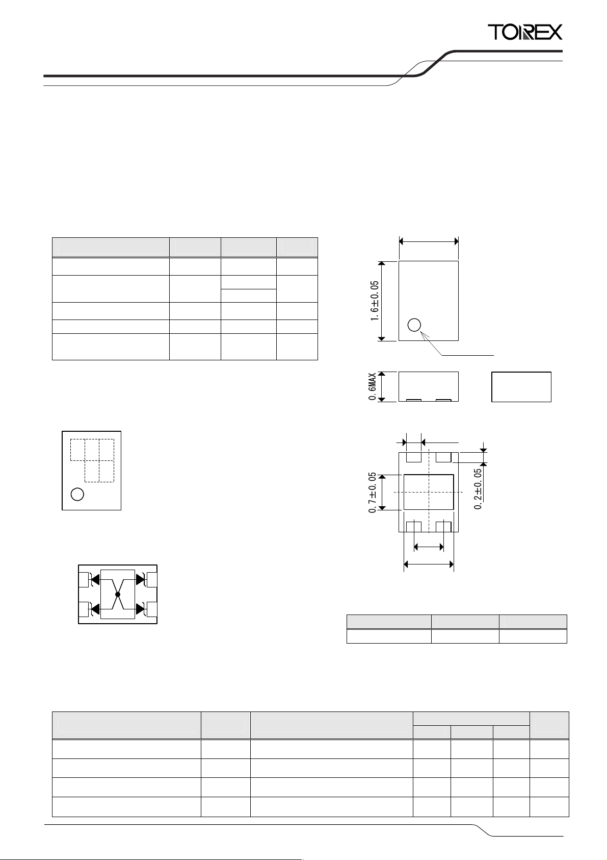
■MARKING RULE
①
■PIN CONFIGURATION
2
1
■ ELECTRICAL CHARACTERISTICS
(*3)(*4)
②③
⑤
④
BOTTOM VIEW
Vpp 30 kV
①②③:BP2(Product Number)
④⑤:Lot Number
3
4
1. Cathode
2. Cathode
3. Cathode
4. Cathode
TAB. Anode
PARAMETER SYMBOL TEST CONDITION
Breakdown Voltage VBR IR =5mA 6.4 6.8 7.2 V
ESD protection
■PACKAGING INFORMATION
■PRODUCT NAME
PRODUCT NAME PACKAGE ORDER UNIT
XBP06V4E4GR-G
*
The “-G” suffix indicates that the products are Halogen and Antimony free
as well as being fully RoHS compliant.
1.2±0.05
1pin INDENT
0.3±0.05
(0.6)
1.0±0.05
*
USP-4 3,000/Reel
LIMITS
MIN. TYP. MAX.
Ta=25℃
UNITS
Leakage Current IRM VRM=5V - - 1.0 μA
Forward Voltage VF IF=10mA - - 1.25 V
Inter-Terminal Capacity Ct VR=0V, f=1MHz - 40 - pF
1/4

XBP06V4E4GR-G
■TYPICAL PERFORMANCE CHARACTERISTICS
(1) Reverse Current vs. Breakdown Voltage (2) Reverse Current vs. Reverse Voltage
100
10
(mA)
R
1
75℃
25℃
1
0.1
(uA)
R
Ta=125℃ 25℃75℃
0.01
BR
Ta=125℃
(V)
0.001
Reverse Current I
0.0001
0123456
Reverse Voltage V
R
(V)
0.1
Reverse Current I
0.01
-25℃
0.001
5.0 5.5 6.0 6.5 7.0 7.5 8.0
Breakdown Voltage V
(3) Breakdown Voltage vs. Operating Temperature (4) Reverse Current vs. Operating Temperature
8.0
10
7.5
(V)
BR
7.0
I
=5mA
1
(uA)
R
-25℃
6.5
0.1
6.0
0.01
Breakdown Voltage V
5.5
5.0
-50 0 50 100 150
Operating Temperature Ta (℃)
Reverse Current I
0.001
-50 0 50 100 150
Operating Temperature Ta (℃)
(5) Inter-Terminal Capacity vs. Reverse Voltage (6) Forward Current vs. Forward Voltage
100
90
80
70
f=1MHz
100
10
(mA)
F
Ta=125℃ 75℃
60
50
1
40
30
20
Inter-Terminal Capacity Ct (pF)
10
0
0123456
Ta=25℃
0.1
Forward Current I
0.01
0 0.2 0.4 0.6 0.8 1 1.2
V
=5.25V
5V
3V
25℃
-25℃
2/4
Reverse Voltage V
R
(V)
Forward Voltage V
F
(V)

p
(
)
■PACKAGING INFORMATION
● USP-4 Power Dissipation
Power dissipation data for the USP-4 is shown in this page.
The value of power dissipation varies with the mount board conditions.
Please use this data as one of reference data taken in the described
condition.
1. Measurement Condition (Reference data)
Condition: Mount on a board
Ambient: Natural convection
Soldering: Lead (Pb) free
Board: Dimensions 40 x 40 mm (1600 mm
Material: Glass Epoxy (FR-4)
Thickness: 1.6 mm
Through-hole: 4 x 0.8 Diameter
Copper (Cu) traces occupy 50% of the board area
in top and back faces.
Package heat-sink is tied to the copper traces.
2
in one side)
2. Power Dissipation vs. Ambient temperature
Board Mount (Tj max = 150℃)
Ambient Temperature (℃)
Power Dissipation Pd (mW)
Evaluation Board (Unit: mm)
Thermal Resistance (℃/W)
XBP06V4E4GR-G
25 1000
150 0
125.00
1200
mW
1000
800
600
ation: Pd
400
Pd-Ta特性グラフ
Pd vs. Ta
200
許容損失Pd(mW)
Power Dissi
0
25 50 75 100 125 150
Ambient Temperature: Ta (℃)
周囲温度Ta(℃)
3/4

XBP06V4E4GR-G
1. The products and product specifications contained he rein are subject to change without
notice to improve performance characteristics. Consult us, or our representatives
before use, to confirm that the information in this datasheet is up to date.
2. We assume no responsibility for any infringement of patents, patent rights, or other
rights arising from the use of any information and circuitry in this datasheet.
3. Please ensure suitable shipping controls (including fail-safe designs and aging
protection) are in force for equipment employing products listed in this datasheet.
4. The products in this datasheet are not developed, designed, or approved for use with
such equipment whose failure of malfunction can be reasonably expected to directly
endanger the life of, or cause significant injury to, the user.
(e.g. Atomic energy; aerospace; transport; combustion and associated safety
equipment thereof.)
5. Please use the products listed in this datasheet within the specified ranges.
Should you wish to use the products under conditions exceeding the specifications,
please consult us or our representatives.
6. We assume no responsibility for damage or loss due to abnormal use.
7. All rights reserved. No part of this datasheet may be copied or reproduced without the
prior permission of TOREX SEMICONDUCTOR LTD.
4/4
 Loading...