

TOREX XB1117 User Manual
■
■
A
■
■
A
XB1117 Series
ETR0315_005a
1A Low Dropout Positive Voltage Regulator
GENERAL DESCRIPTIO N
The XB1117 series is 1A Bi-polar transistor LDO voltage regulator. Output volt age of the XB1117P series is fixed to 1.8V, 2.5V,
3.3V, and 5.0V. The XB1117K series output voltage is adjustable by the external resistors. Pleas e refer to the absolute
maximum ratings for the difference between the rated input voltage of the XB1117P50 (V
K12B. With the dropout voltage 1.2V (TYP.), output current can be generated up to 1A. The built-in overcurrent circuit and
thermal protection circuit start to operate when either one of output put current reaches the current limit level or ju nction
temperature reaches the temperature limit. The XB1117 series provide stable line and load regulation by using an input
capacitor and an output capacitor (10μF, tantalum). Package is available in SOT-223.
PPLICATIONS
●Highly efficient linear regulators
●5V ~ 3.3V DC / DC converter
●Battery charger
●Local power supply inside equipment
●Battery powered equipment
FEATURES
Maximum Output Current : 1A
Output Voltages : 1.8V, 2.5V, 3.3V, 5.0V, ADJ
Output Voltage Accuracy : ±1%
Low Dropout Voltage : 1.2V @ IOUT=1A
Line Regulation (TYP.) : 0.04% (ADJ)
Load Regulation (TYP.) : 0.1% (ADJ)
djust Pin Current : Less than 120μA (ADJ)
Protection Circuit :
Package : SOT-223
Environmentally Friendly : EU RoHS Compliant, Pb Free
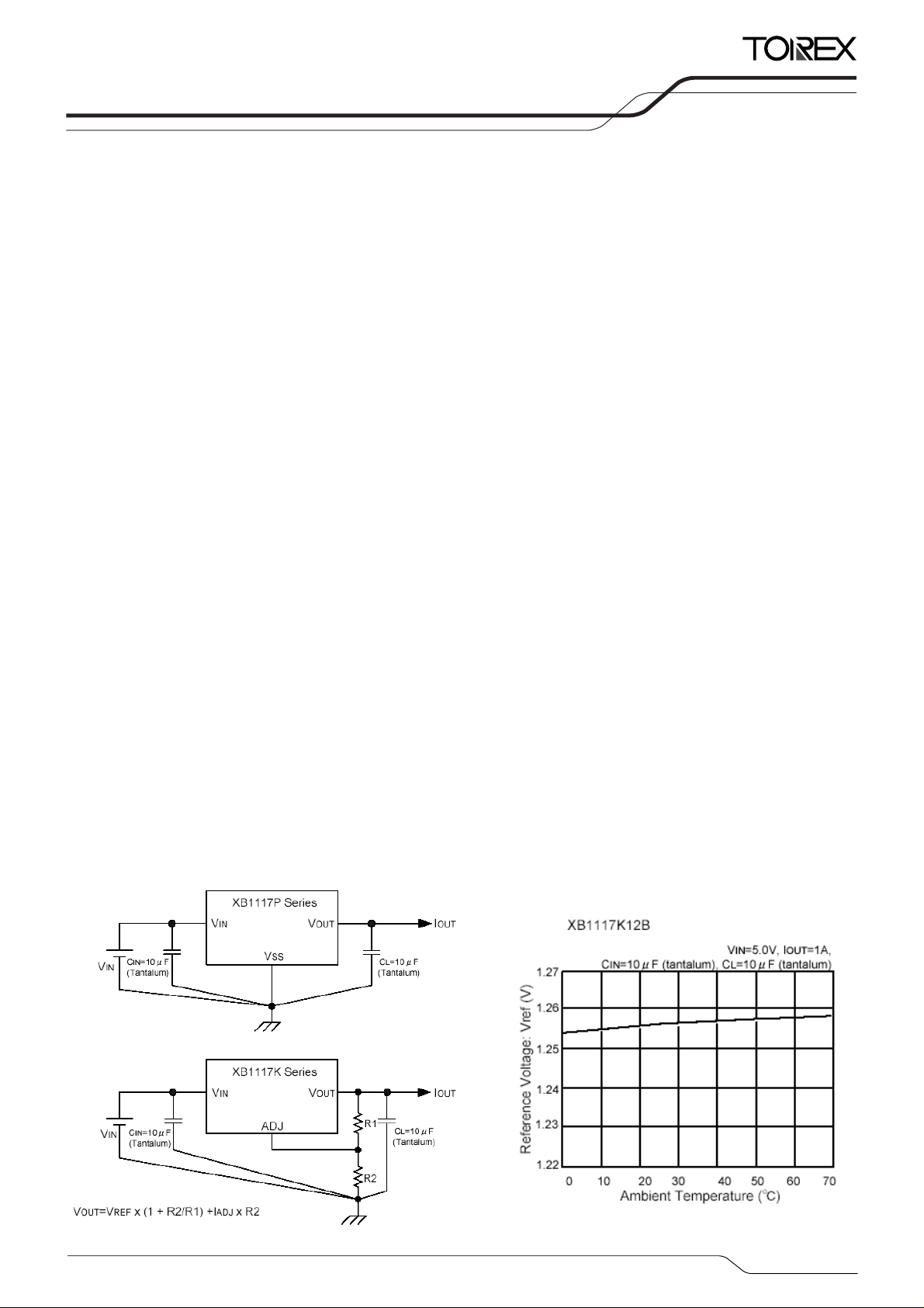
TYPICAL APPLICATION CIRCUIT
■TYPICAL PERFORMANCE
CHARACTERISTICS
●Reference Voltage vs. Ambient Temperature
OUT=5.0V) and XB1117P18, 25, 31,
Over-current pr ot ection
Thermal protecti o n
1/12
■
■
■
XB1117 Series
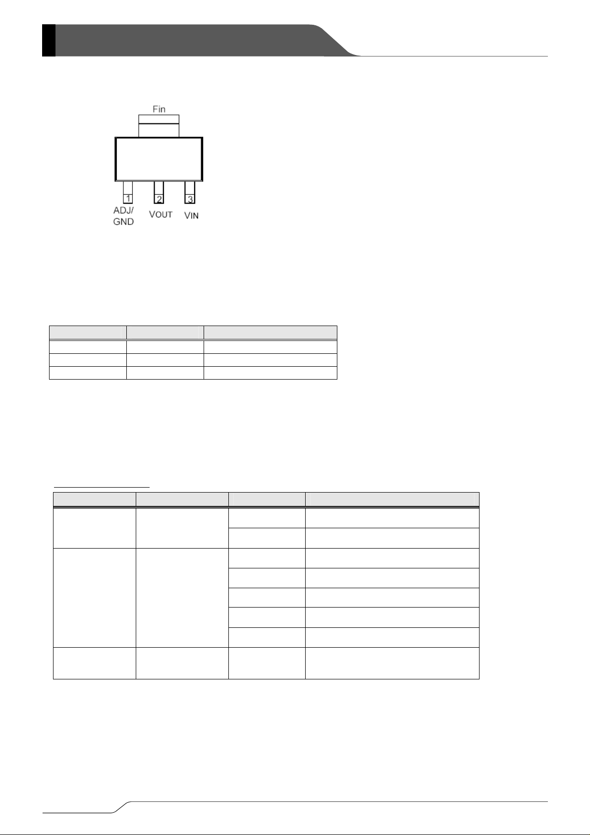
PIN CONFIGURATION
PIN ASSIGNMENT
PIN NUMBER PIN NAME FUNCTIONS
1 ADJ/GND ADJ/Ground
2 VOUT Output
3 VIN Input
* The electrical potential of the package fin is the same as the VOUT pin.
PRODUCT CLASSIFICATION
●Ordering Information
XB1117①②③④⑤⑥-⑦
DESIGNATOR DESCRIPTION SYMBOL
①
②③④
⑤⑥-⑦
(*1)
The “-G” suffix indicates that the products are Halogen and Antimony free as well as being fully RoHS compliant.
(*2)
The device orientation is fixed in its embossed tape pocket. For reverse orientation, please contact your local Tore x
sales office or representative. (Standard orientation: ⑤R-⑦, Reverse orientation: ⑤L-⑦)
SOT-223
(TOP VIEW)
(*1)
Type of Regulators
Output Voltage
& Accuracy
Packages
Taping Type
(*2)
DESCRIPTION
P Fixed VOUT type
K Adjustable V
181
251
331
501
12B
FR-G SOT-223
Fixed V
Fixed V
Fixed V
Fixed V
Adjustable V
OUT type
OUT 1.80V (±1%)
OUT 2.50V (±1%)
OUT 3.30V (±1%)
OUT 5.00V (±1%)
OUT 1.25V (±1%)
2/12
■
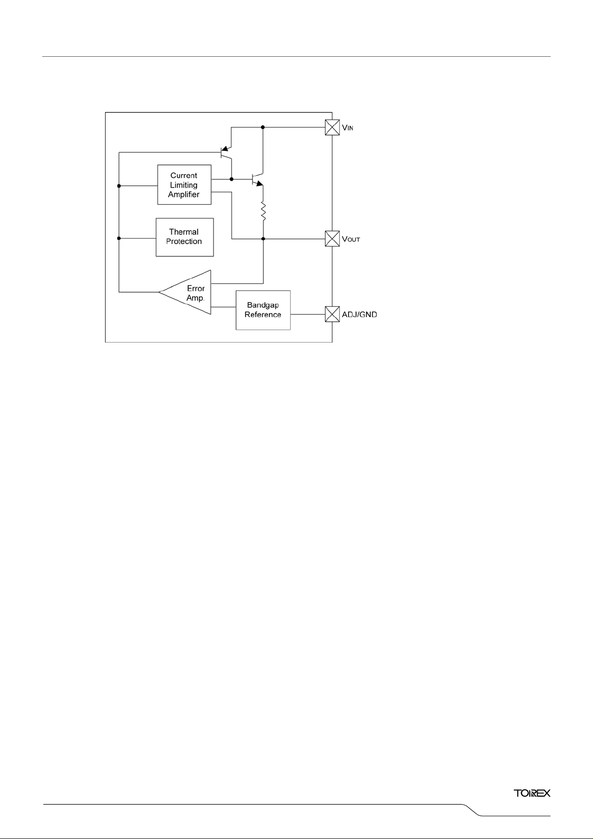
BLOCK DIAGRAM
XB1117
Series
3/12
■
A
■
XB1117 Series
BSOLUTE MAXIMUM RATINGS
XB1117P501
PARAMETER SYMBOL RATINGS UNITS
Input Voltage VIN 10.0 V
Thermal Resistance
(Junction to Case)
Thermal Resistance
(Junction to Ambient)
Power Dissipation
(ΔT=100℃)
C
θJ
θJ
A
PD 625 mW
Operating Temperature Range Topr
Operating Junction Temperature Range Tj
Storage Temperature Range Tstg
Lead Temperature Tlead 260
*Stress above the listed absolute maximum rating may cause permanent damage to the device.
** The rated values of the XB1117P18 / 25 / 30 (V
of the XB1117P50 (V
OUT=5.0V).
OUT=1.8V, 2.5V and 3.0V) and XB1117K type are different from that
15
160
0 ~+70
0 ~+125
- 65 ~+150
ELECTRICAL CHARACTERISTICS
XB1117P501
℃/W
℃
Ta=25℃
PARAMETER SYMBOL CONDITIONS MIN. TYP. MAX. UNITS
Output Voltage VOUT
Line Regulation
Load Regulation
ΔV
ΔV
OUT1
OUT2
Dropout Voltage Vdif
Current Limit ILIM
Supply Current ISS
Temperature
Coefficient
TC
Temperature Stability TS
*Over Temp. = Over Temperature(0〜+70℃)
VIN=7.0V
I
OUT=0A
7.0V≦VIN≦9.0V
OUT=0A
I
V
IN=7.0V
OUT≦1.0A
0A≦I
OUT=±1%
ΔV
0A≦I
OUT≦1.0A
7.0V≦V
IN≦10.0V
VIN=7.0V
0A≦I
OUT≦1.0A
7.0V≦V
0A≦I
IN≦10.0V
OUT≦1.0A
VIN=7.0V
I
OUT=100mA
4.950 5.000 5.050
*Over Temp. 4.900 5.000 5.100
V
*Over Temp. - 1 6
- 5.0 15.2
mV
*Over Temp. - 10.1 20.2
- 1.2 1.4
*Over Temp. - 1.3 -
V
*Over Temp. 1.0 1.5 - A
*Over Temp. - 6 13 mA
- 50 -
*Over Temp. - 0.5 -
ppm/℃
%
4/12
 Loading...