


TOPLINKST TECHNOLOGY COMPANY LIMITED
UNIT 04,7F,BRIGHT WAY TOWER, NO,33 MONG KOK ROAD, KOWLOON, Hong Kong
IEEE 802.11 a/b/g/n
300Mbps WiFi Module
Product Specifications
Model: TOP-S5
Version: 1.1
2015-12-15
Information in this document is subject to change without prior notice. Page 1 of 13
1. Introduction
The TOP-S5 is a WLAN module supporting IEEE 802.11a/b/g/n standards with 7-pin or 4-pin
connector supporting USB2.0 interface. This is a small form factor and low cost compact WLAN module
designed for the wireless connectivity. This module operates in 2.4GHz and 5GHz dual band frequency ,
it applies a highly integrated MAC/BBP and RF/PA/LNA single chip RT5572 with 300Mbps PHY rate
supporting. It fully complies with IEEE802.11n draft 3.0 and IEEE802.11a/b/g feature.
2. Features
20MHz/40MHz bandwidth, support 2T2R mode in 2.4GHz and 5GHz .
802.11a: 6, 9, 12, 24, 36, 48, 54Mbps; 802.11b: 1, 2, 5.5, 11Mbps; 802.11g: 6, 9, 12, 24, 36, 48,
54Mbps ; 802.11n: Support PHY rate up to 300Mbps.
Support Soft-AP; QoS-WMM, WMM-PS; WiFi Direct;
WPS pin, LED indicates WiFi link & activity;
Multiple BSSID support; Power management.
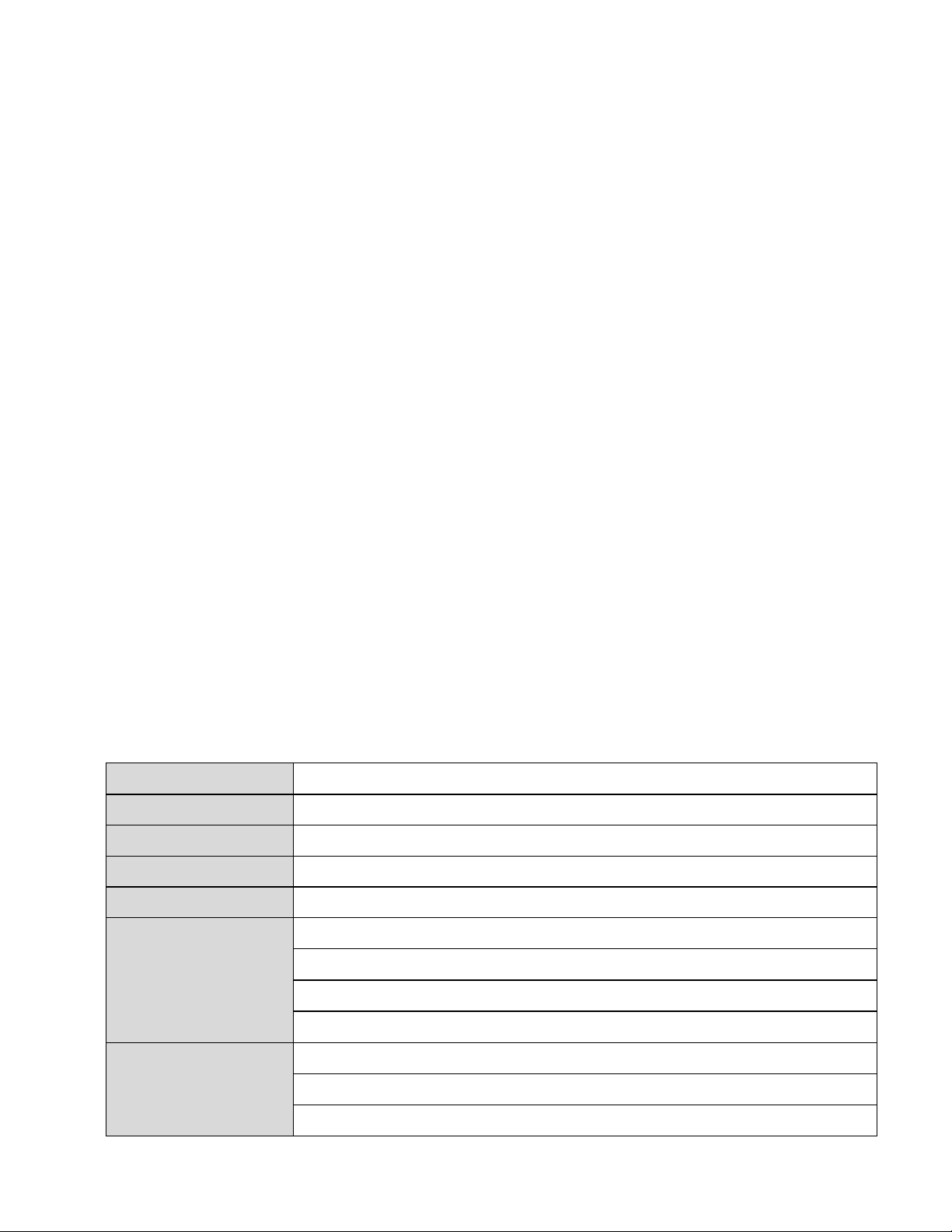
3. Product Information
3.1 Specification (Typical Value):
Main Chipset
Operation Frequency
Protocols
Antennas
Security
Typical Transmit
Power
(Antenna feed point)
Ralink RT5572N
2412~2483.5MHz,4.915~5.825GHz (
802.11b: CCK, QPSK, BPSK, 802.11a/g/n: OFDM
Two outputs to two dual band external antennas
WEP 64/128, WPA/WPA2/WAPI, TKIP/AES; WPS/WPS2:PIN,PBC
802.11b (CCK) 11Mbps: 17+/-1dBm
802.11g (OFDM) 54Mbps: 15+/-1dBm
802.11a (OFDM) 54Mbps: 11+/-1.5dBm
802.11n (HT20@MCS7), 13+/-1dBm; (HT40@MCS7),12+/-1dBm
Different country adopts different frequency)
802.11b: -88+/-1dBm; 802.11g: -73+/-1dBm
Receive Sensitivity
(Antenna feed point)
802.11n (HT20), -71+/-1dB m; 802.11n (HT40), -68+/-1dBm
802.11a: -70+/-1dBm
Information in this document is subject to change without prior notice. Page 2 of 13
Operating
Voltage/current
5.0VDC ± 5% ; <350mA @802.11n,HT40 ; or 3.3VDV± 5% <500mA, @802.11n,HT40
5.0VDC ± 5% ; <450mA @802.11a,HT40 ; or 3.3VDV± 5% <630mA, @802.11a,HT40
Host interface
Interface
Dimensions/Weight
USB 2.0
7-pin or 4-pin, 2.0mm , or 4-pin 2.54 mm pitch pin header
48x18mm / 3.6g
3.2 Block Diagram
Figure 1: System Block Diagram of 7 pin TOP-S5 5.0V WLAN Module
3.3V/1.5V 5V/3.3V
RT5572
USB
Interface
VCC(5.0V)
DM(DATA-)
DP(DATA+)
GND
TX CONTROL
EXTERNAL LED
WPS CONTROL
USB
Interface
Baseband
MAC/
Packet
Buffer/
Encrption
Engine
RF
Transmitter
RF
Receiver
40MHz XTAL
LNA
PA
2.4G/5GHz
Duplexer
2.4G/5GHz
Duplexer
Antenna
Dual Band
External antennas
2.412~2.4835GHz
4.915~5.825 GHz
Antenna
Figure 2: System Block Diagram of 7 pin TOP-S5 3.3V WLAN Module
3.3V/1.5V
RT5572
USB
Interface
VCC(3.3V)
DM(DATA-)
DP(DATA+)
GND
TX CONTROL
EXTERNAL LED
WPS CONTROL
USB
Interface
Baseband
MAC/
Packet
Buffer/
Encrption
Engine
RF
Transmitter
RF
Receiver
40MHz XTAL
LNA
PA
2.4G/5GHz
Duplexer
2.4G/5GHz
Duplexer
Antenna
Dual Band
External antennas
2.412~2.4835GHz
4.915~5.825 GHz
Antenna
Information in this document is subject to change without prior notice. Page 3 of 13
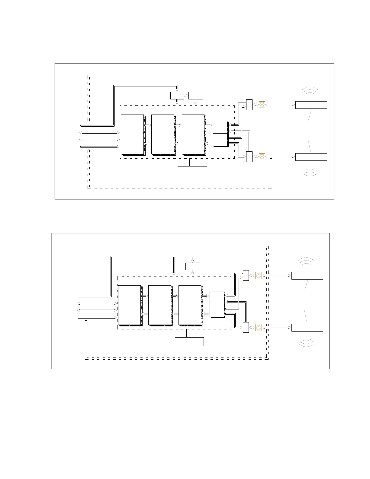
Figure 3: System Block Diagram of 4 pin TOP-S5 5.0V WLAN Module
2.4G/5GHz
3.3V/1.5V 5V/3.3V
RT5572
Duplexer
Antenna
USB
Interface
VCC(5.0V)
DM(DATA-)
DP(DATA+)
GND
USB
Interface
Baseband
MAC/
Packet
Buffer/
Encrption
Engine
RF
Transmitter
RF
Receiver
40MHz XTAL
LNA
PA
Figure 4: System Block Diagram of 4 pin TOP-S5 3.3V WLAN Module
2.4G/5GHz
Duplexer
2.4G/5GHz
Duplexer
USB
Interfac e
VCC(3.3V)
DM(DATA-)
DP(DATA+)
GND
USB
Interface
RT5572
Baseband
MAC/
Packet
Buffer/
Encrption
Engine
3.3V/1.5 V
RF
Transmitter
RF
Receiver
40MHz XTAL
LNA
PA
2.4G/5GHz
Duplexer
Dual Band
External antennas
2.412~2.4835GHz
4.915~5.825 GHz
Antenna
Antenna
Dual Band
External antennas
2.412~2.4835GHz
4.915~5.825 GHz
Antenna
Information in this document is subject to change without prior notice. Page 4 of 13
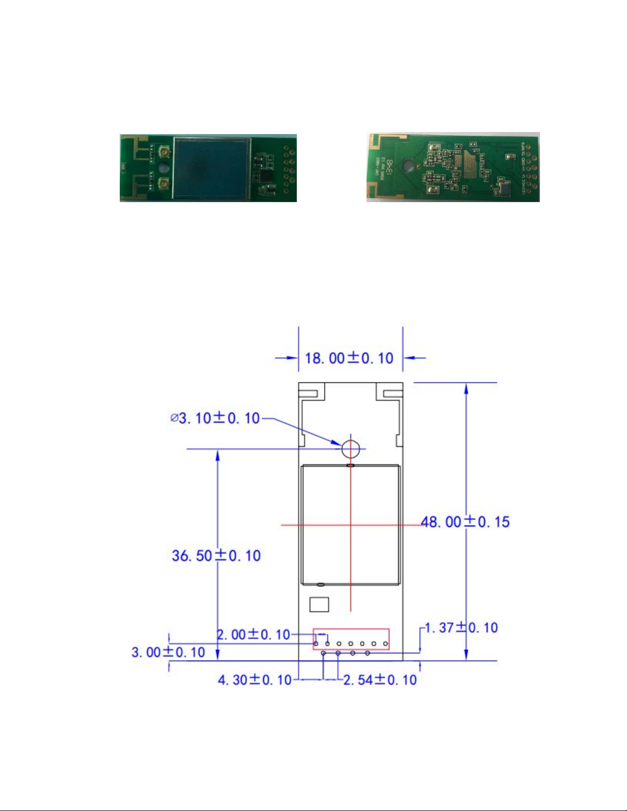
3.3 Mechanical Information
3.3.1 OUTLINE and Connection Interface (Pictures are for reference only)
Figure 5: 5.0VDC power input module.
Information in this document is subject to change without prior notice. Page 5 of 13

RF connector at bottom
Figure 6: General Dimensions
RF connector at top
Figure 7: General Dimensions
Information in this document is subject to change without prior notice. Page 6 of 13

3.3.1.1 4-pin 2.54 mm pitch pin header.
a). Model: TOP-S5, 4M02
Figure 8:Bottom side 4–Pin 2.54mm pitch pin header interface.
3.3.1.2 4-pin 2.0 mm pitch pin header
a). Model: TOP-S5, 4M02
Information in this document is subject to change without prior notice. Page 7 of 13

Figure 10: Bottom side 4–Pin 2.0mm pitch pin header interface.
3.3.1.3 7-pin 2.0 mm pitch pin header and RF connector at top side
a). Model: TOP-S5, 4M02
Information in this document is subject to change without prior notice. Page 8 of 13

Figure 12: Top side 7–Pin 2.0mm pitch pin header interface.
Tips:
For details model number, please refer to the ordering information.
Information in this document is subject to change without prior notice. Page 9 of 13

Pin Definition:
Pin-out 7-pin 2.0mm pitch pin header 4-pin 2.0 or 2.54mm pitch pin header
1
2
3
4
5
6
7 WPS control
LED* (Wireless TX status) N/A
VCC (3.3 VDC or 5.0VDC) VCC (3.3 VDC or 5.0VDC)
U- (USB data+) U- (USB data+)
U+ (USB data-) U+ (USB data-)
GND (Ground) GND (Ground)
RF/TX ON/OFF control N/A
N/A
Figure 16: The onboard circuit configuration refer to LED, WPS, TX pinout.
Notes:
TX or WPS pin is internally pulled up with an onboard 4.7K ohm resistor to 3.3VDC .It is low level
(can be connected to ground) activated.
LED outputs 3.3V blink signal, the LED operation current is limited via the 330 ohm resistor.
If the onboard and external LEDs must be used simultaneously, proper LEDs’ operation current
must be considered, If necessary, the internal onboard LED can be removed while ordering.
Information in this document is subject to change without prior notice. Page 10 of 13

I
3.4 R
F
P
t
t
a
o
O
c
o
n
X
s
m
a
0
u
n
p
e
o
h
o
o
i
m
u
a
P
P
o
r
o
2
o
DAAAA
e
or
r
g
If the I RF outpu
output C
EX RF con
via an I-PE
nnection I
ection is se
MHF rece
formation
lected, a 50
tacle (RF c
ohm extern
nnector). (
l antenna c
art No.: 20
nnects to th
79-001E-01
module
).
Figur
17:The pr
file of the I-
EX connect
Figure 18:
3.5 Sof
Oper
Linux
Wind
Mac
Andro
nformation
ware and
tion Syste
2.4/2.6
ws XP/Vist
id 4.0
S X 10.4~1
in this do
ystem Inf
/7/8
.8
ument is s
rmation
CPU Suppl
ARM, MIPS
X86 Platfor
N/A
N/A
bject to c
Typical RF
e
II
ange witho
utput type
t prior no
rive
vailable
vailable
vailable
vailable
tice.
Pa
e
11 of 13

3.6 Ordering information
Since there are many different types of pin header might be used, such as: straight pin; 90 degree
bend pin; long pin; short pin…, please mention the detail requirement of the pin header when
ordering. It can be mentioned by part number or by descriptions.
4 Agency Approval
CAUTION:
Agency Operative standards Certificate ID
FCC Part15 C OET65 ZLJTOP-S5
EN60950 EN301489
CE
EN300328 EN62479
Pre-scan undergoing
√
RoHS 2011/65/EC
Information in this document is subject to change without prior notice. Page 12 of 13

5 Environment pointer
Special Instructions:
Since the 5.0GHz operating current is High, in order to ensure that products -10 º C to +50 º C working
properly, must be added the heat sink;
If the customer wants to have a better product performance, it is necessary to replace the heat sink thermal
performance better (The thicker the larger the area the better the thermal performance).
Item category Range
Temperature Operating Temperature -10ºC to +50ºC
Storage Temperature -20ºC to +80ºC
Humidity Operating Humidity Conditions
Non-Operating Humidity Conditions
(including warehouse)
The range of 20% to 80%
(non-condensing) .
The range of 20% to 80%
6 Disclaimer
THESE MATERIALS AND INFORMATION ARE PROVIDED “AS IS” WITHOUT WARRANTY OF ANY
KIND, EITHER EXPRESS OR IMPLIED , INCLUDING BUT NOT LIMITED TO, THE IMPLIED
WARRANTIES OF MERCHANTABILITY, FITNESS FOR A PARTICULAR PURPOSE OR
NON-INFRINGEMENT.
We use reasonable efforts to include accurate and up-to-date information on this document; it does not,
however, make any representations as to its accuracy or completeness of the information, text, graphics,
links or other items contained within these materials. You use this document to bear the risk of their own.
Ogemray,as its suppliers, and other parties involved in creating and delivering this Document’s contents
shall not be liable for any special, indirect, incidental, or consequential damages, including without limitation,
lost revenues or profits.
To comply with FCC RF exposure limits, it is recommended that for the wireless adapter installed in a host
computer , the low gain integrated antennas for this device should be located at a minimum separation
distance from the body of all persons as specified according to the FCC modular grant conditions.
Information in this document is subject to change without prior notice. Page 13 of 13

FCC Statement
Federal Communication Commission Interference Statement
This equipment has been tested and found to comply with the limits for a Class B digital device, pursuant to Part 15 of the
FCC Rules. These limits are designed to provide reasonable protection against harmful interference in a residential
installation. This equipment generates, uses and can radiate radio frequency energy and, if not installed and used in accordance
with the instructions, may cause harmful interference to radio communications. However, there is no guarantee that interference
will not occur in a particular installation. If this equipment does cause harmful interference to radio or television reception,
which can be determined by turning the equipme nt of f and on, the user is encouraged to try to correct the interference by one
of the following measures:
- Reorient or relocate the receiving antenna.
- Increase the separation between the equipment and receiver.
- Connect the equipment into an outlet on a circuit different from that to which the receiver is connected.
- Consult the dealer or an experienced radio/TV technician for help.
FCC Caution:
Any changes or modificati ons not expressly approved by the party responsible f or c ompliance could void the user's authority
to operate this equipment.
This device complies with Part 15 of the FCC Rules. Operation is subject to the following two conditions:
(1) This device may not cause harmful interference, and
(2) This device must accept any interference received, including inte rference that may cause undesired operati o n.
The TOP-S5 module is for OEM integrations only. The end-user product will be professionally installed in such a manner
that only the authorized antennas are used Any changes or modifications NOT explicitly APPROVED by TOPLINKST could
cause the module to cease to comply with FCC rules part 15, and thus void the user's authority to operate the equipment.
FCC Radiation Exposure Statement:
This equipment complies with FCC radiation exposure limits set forth for an uncontrolled environment. This transmitter
module must not be co-located or operating in conjunction with any oth er antenna or transmitter.
The wireless adapter is not designed for use with high-gain directional antennas. Use of such antennas with these products
in a manner other than as described in the following section titled, "Antenna Use" is illegal
Antenna Use
This device is used printed antenna, the max antenna gain is 2.0dBi
IMPORTANT NOTE:
In the event that these conditions can not be met (for example certain laptop configur atio ns or co-location with another transmitter),
then the FCC authorization is no longer c o nsidered valid and the FCC ID can not be used on the final product. I n the se circumstances,
the OEM integrator will be responsible for re-evaluating the end product (including the transmitter) and obtaining a
separate FCC authorizatio n.
End Product Labeling
The final end product must be labeled in a visible area with the following: “Contains FCC ID:
Manual Information to the End User
The OEM integrator has to be aware not to provide information to the end user regarding
how to install or remove this RF module in the user’s manual of the end product which
integrates this module.
This device is restricted indoor environment only.
ZLJTOP-S5”.

Notes:
Important
After integrating this modular approved transmitter according to these instructions in this
following points have to be
manual,
considered:
- The end-product incl. this modular approved transmitter must comply with the FCC
host
manufacturer/integrator
is required to show compliance with 15B (§15.107 + 15.109)
module is installed and operating. In addition, the module should be transmitting and
should confirm that the module’s intentional emissions (15 C) are still
out-of-band emission). Verify that there are no additional unintentional
permitted in 15B or emissions compliant with the transmitter rule. Any
emissions are unintentional which means that the host is not
compliant.
compliant
emissions
additional
regulations. The
while
the
evaluation
(fundamental and
other than what is
non-compliant
- Additional antennas may be used with this modular approved transmitter, provided they are
same type, have equal or less gain and have identical in- and outband characteristics as the
ones. Other antenna types or antennas with higher gain require appropriate equipment
authorization.
from
certified
- Due to its output power the integration is strictly limited into mobile/fixed categorized host
and the user manual of the host device has to include appropriate RF exposure
information/warning.
devices
- Any modifications made to the module will void the Grant of Certification, this module is limited
OEM installation only and must not be sold to end-users, end-user has no manual instructions
remove or install the device, only software or operating procedure shall be placed in the
operating manual of final
products.
- This modular approved transmitter is approved for stand-alone configurations only. For
simultaneous transmission with additional transmitters follow the FCC Multi-transmitter policy.
end-user
the
to
to
 Loading...