

TOKOM KV1560NT Datasheet
KV1560NT
VARIABLE CAPACITANCE DIODE
FEATURES
■ Very Wide Operating Voltage Range (1 to 8 V)
■ Excellent Linearity (CV Curve)
■ Large Capacitance Ratio (A = 17 minimum)
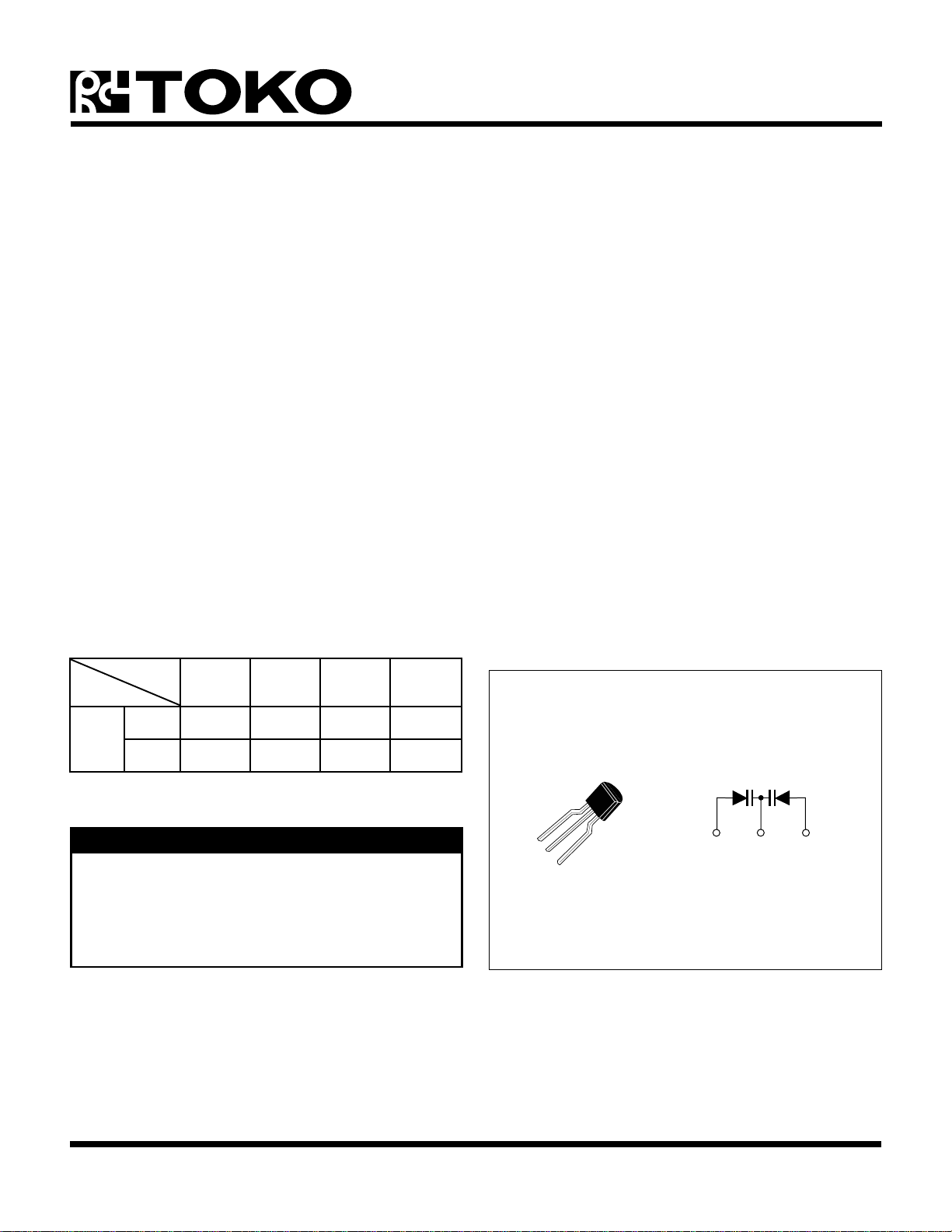
■ Two Diodes in a 3 Lead Through-Hole Discrete
Package (TO92-3)
■ Very Small Capacitance Deviation at Tape/Reel
DESCRIPTION
The KV1560NT variable capacitance diode is well-suited
for use in all types of VFO and VCO, as well as radio
cassettes, stereos, and car radios.
The KV1560NT has a high degree of matching
characteristics.
The KV1560NT is housed in a TO92-3 package.
CLASSIFICATION
(Unit: pF)
APPLICATIONS
■ AM Radio
■ Voltage Controlled Oscillator
RANK
C
MIN 428.00 446.00 464.00 482.00
C
1
MAX 452.00 470.00 488.00 506.00
1234
ORDERING INFORMATION
KV1560NT
Note: The KV1560NT is supplied on folded paper tape (25 pieces per fold),
1500 pcs per box.
KV1560NT
150
123
August 1999 TOKO, Inc. Page 1

KV1560NT
ABSOLUTE MAXIMUM RATINGS
Reverse Voltage....................................................... 16 V
Forward Current .................................................... 50 mA
Power Dissipation .............................................. 100 mW
ELECTRICAL CHARACTERISTICS
Test conditions: T
SYMBOL PARAMETER TEST CONDITIONS MIN TYP MAX UNITS
= 25 °C
A
Storage Temperature Range ................... -55 to +150 °C
Operating Temperature Range ...................-55 to +85 °C
Lead Soldering Temperature (10 s) ......................235 °C
V
REV
I
REV
C
1
C
8
∆C1.0
∆C4.5
∆C8.0
Q Quality Factor V
A Capacitance Ratio C
Note 1: Diode Capacitance measured with HP 4279A or equivalent instruments (at OSC level 20 mVrms, ± 5 mVrms).
Note 2: ∆C = X 100 *D1, D2: Please refer to the Pin Layout shown below.
Reverse Voltage I
Reverse Current V
Diode Capacitance 1 V
Diode Capacitance 8 V
Capacitance Tolerance
(Note 2)
Cmax (D1, D2) - Cmin (D1, D2)
Cmin (D1, D2)
= 10 µA16V
REV
= 10.0 V 100 nA
REV
= 1.0 V, f = 1 MHz 428.00 506.00 pF
REV
= 8.0 V, f = 1 MHz 20.00 27.50 pF
REV
V
= 1.0 V, f = 1 MHz 1.0 %
REV
V
= 4.5 V, f = 1 MHz 2.0 %
REV
V
= 8.0 V, f = 1 MHz 2.0 %
REV
= 1.0 V, f = 1MHz 200
REV
/ C
1
8
Symbol Anode Pin
Cathode
17.00
Pin
Diode 1 D
Diode 2 D
1
2
12
32
Page 2 August 1999 TOKO, Inc.
 Loading...