TOKO TK73200MCL Datasheet

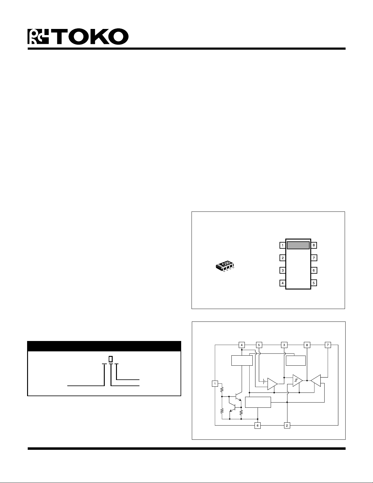
TK73200
C
PULSE
CONTROL
GND
BASE
NOISE
BYPASS
V
ADJ
I
PK
V
IN
ADJUSTABLE LOW DROPOUT REGULATOR
FEATURES
■ Up to 5 A Output Current Capability with External
PNP Transistor
■ Internal Short Circuit Protection
■ Excellent Load Regulation
■ CMOS/TTL-Compatible On/Off Switch
■ Internal Reverse Bias Current Protection Switch
■ Internal Thermal Shutdown
■ Wide Adjustable Output Voltage Range
(2.0 V to 12.0 V)
■ Continuous and Pulsed Current Modes
DESCRIPTION
The TK73200 is a controller IC for an adjustable low
dropout voltage regulator. The TK73200 and the external
PNP power transistor provide adjustable output voltages
from 2 to 12 V and output current from 100 mA to 5 A. By
utilizing an external PNP power transistor, low dropout
voltage at high current can be readily achieved. The
internal electronic switch can be controlled by TTL or
CMOS logic levels. The device is in the “on” state when the
control pin is pulled to a high logic level. A pin for a bypass
capacitor, which connects to the internal circuitry, is
provided to lower the overall output noise level.
APPLICATIONS
■ Battery Powered Systems
■ Cellular/Cordless Telephones
■ Radio Control Systems
■ Wireless Communications Systems
■ Portable Instrumentations
■ Portable Computers
■ Personal Digital Assistants
■ Local Area Network (LAN) Receivers
■ Power Recovery for Microprocessors
TK73200
The current limit characteristics can be configured as
continuous (constant current) or pulsed (cycling). An
internal thermal shutdown circuit limits the junction
temperatures to below 150 °C.
BLOCK DIAGRAM
I
IN
PK C
PULSE
V
BASE
V
ORDERING INFORMATION
TK73200M L
Tape/Reel Code
Package Code
TAPE/REEL CODE
L: Tape Left
TEMP. RANGE
C: -30 to 80 °C
June 1999 TOKO, Inc. Page 1
Temp. Code
PACKAGE CODE
M: SOT23L-8
CONTROL
ON/OFF
CIRCUIT
BANDGAP
REFERENCE
GND
THERMAL
SENSOR
NOISE BYPASS
ADJ

TK73200
ABSOLUTE MAXIMUM RATINGS (NOTE 5)
Supply Voltage Range ............................................ 19 V
Power Dissipation (Note 1) ................................ 600 mW
Reverse Bias Voltage Range ..................................... 6 V
Noise Bypass Pin Terminal Voltage Range ............... 5 V
Control Pin Terminal Voltage Range........................ 14 V
Storage Temperature Range ................... -55 to +150 °C
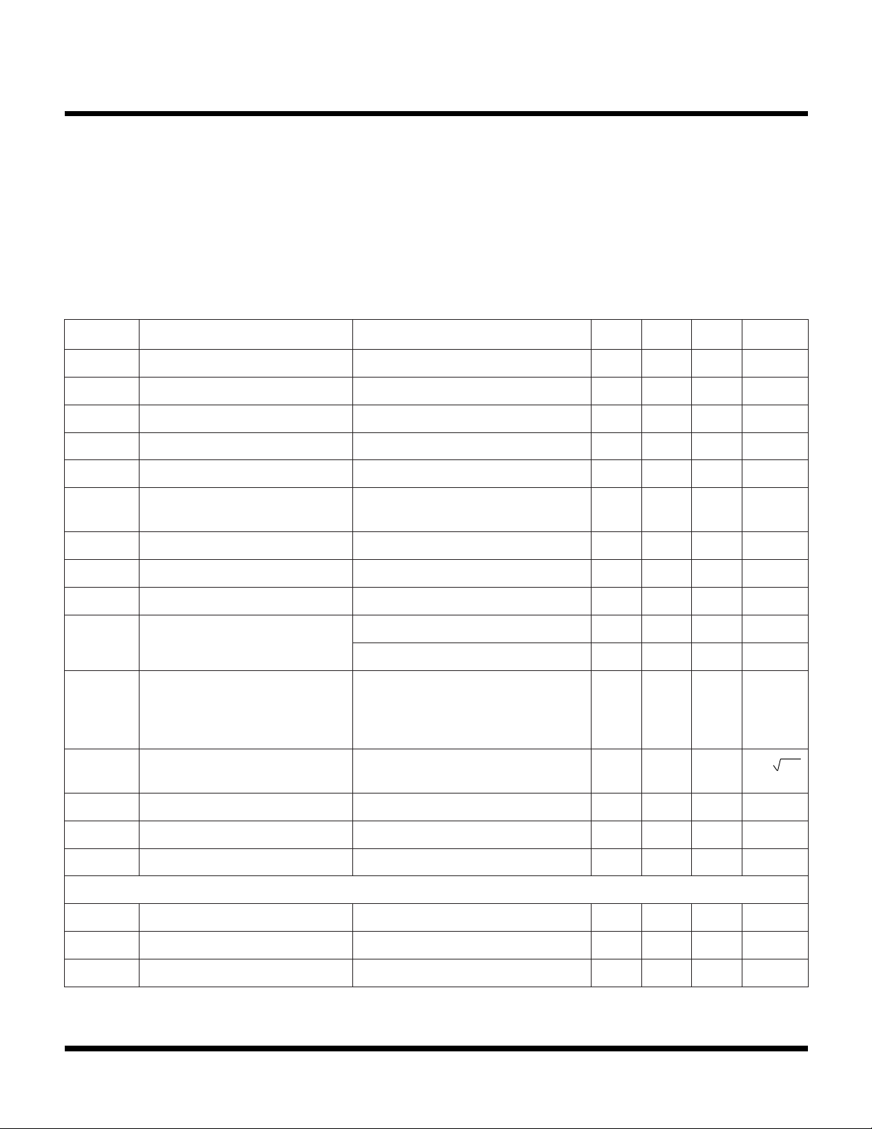
TK73200 ELECTRICAL CHARACTERISTICS
Test conditions: VIN = V
LOBMYSRETEMARAPSNOITIDNOCTSETNIMPYTXAMSTINU
OUT(TYP)
+ 1 V, TA = 25 °C, unless otherwise specified.
Operating Temperature Range ...................-30 to +80 °C
Extended Temperature Range................... -40 to +85 °C
Operating Voltage Range............................ 1.8 to 14.0 V
Junction Temperature ........................................... 150 °C
Lead Soldering Temperature (10 s) ...................... 235 °C
I
Q
I
YBTS
I
TUO
V
PORD
V
TUO
geReniLnoitalugeReniL
I
)L(ESAB
I
)H(ESAB
V
ESNES
RRnoitcejeRelppiR
V
ON
tnerruCtnecseiuQI
tnerruCybdnatSV
TUO
NI
IgnidulcxE,Am0=
TNOC
052063Aµ
FFOtuptuO,V8=1.0Aµ
tnerruCtuptuOtnednepeDrotsisnarTlanretxEA/NA
egatloVtuoporDtnednepeDrotsisnarTlanretxEA/NV
egatloVtuptuOsrotsiseRlanretxEybteS221V
V=
V
NI
V
)PYT(TUO
)PYT(TUO
otV1+
)2etoN(V6+
0.302Vm
geRdaoLnoitalugeRdaoLtnednepeDrotsisnarTlanretxE01Vm
WOLtnerruCesaBV8.1 ≤ VNI≤ V451Am
HGIHtnerruCesaBV1.4 ≤ VNI≤ V2104Am
edoMtimiLtnerruCsuounitnoC08001021Vm
egatloVtceteDtimiLtnerruC
edoMtimiLtnerruCesluP0709011Vm
C,zH004=f
L
C
N
I
TUO
V,Fµ1.0=
NI
V,Am03=
,Fµ01=
V=
)PYT(TUO
ELPPIR
,V5.1=
,smrVm001=
75Bd
)3etoN(
esioNtuptuO
)3etoN(
,zHk03otzH004=FPB,zHk1=f
31.0zH/Vµ
I
∆V
V
/∆T
C
ESLUP
egatloVecnerefeR 22.152.182.1V
ESLUP
TUO
fer
tnerruClanimreTniP)4etoN(515254Aµ
tneiciffeoCerutarepmeT 02C°/mpp
SNOITACIFICEPSLANIMRETLORTNOC
I
TNOC
V
V
)NO(TNOC
)FFO(TNOC
tnerruClortnoCV
TNOC
)NO(egatloVlortnoCNOtuptuO8.1V
)FFO(egatloVlortnoCFFOtuptuO6.0V
NOtuptuO,V8.1=5.602Aµ
Page 2 June 1999 TOKO, Inc.

TK73200
TK73200 ELECTRICAL CHARACTERISTICS (STANDARD DEVICES) CONT.
Note 1: Power dissipation is 600 mW when mounted as recommended. Derate at 4.8 mW/°C for operation above 25 °C.
Note 2: Refer to: “Definition of Terms.”
Note 3: Ripple rejection and noise voltage are affected by the value and characteristics of the capacitor used.
Note 4: This pin is used for Pulse Current Limit Mode. When selecting Continuous Current Limit Mode, this pin is connected to GND.
Note 5: The voltage applied to any pin must be greater than -0.4 V.
Gen. Note: Parameters with min. or max. values are 100% tested at TA = 25 °C.
June 1999 TOKO, Inc. Page 3

TK73200
V
(
0
V/
DIV)
V
(10
V/
DIV)
V
(
V/
DIV)
I
(
A)
V
(
V)
I
(
A)
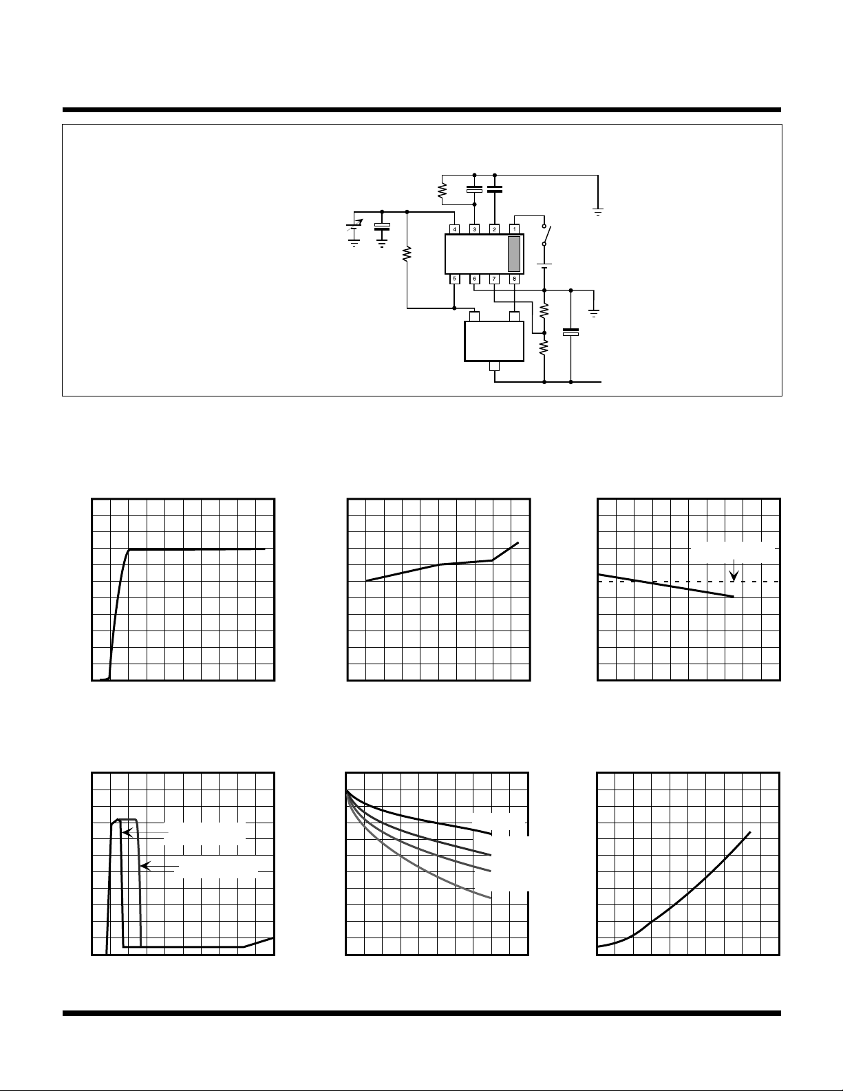
Note:Transistor: 2SB1115
TEST CIRCUIT
CPC
N
R
P
V
IN
CN = 0.1 µF
CP = 0.1 µF
C
IN
R
IPK
TK73200
CONT
CIN = 1 µF
CL = 4.7 µF
RP = 330 k
Continuous Current Limit Mode:
I
(mA) = 100 mV / R
SET
Pulse Current Limit Mode:
I
(mA) = 90 mV / R
SET
IPK
IPK
(Ω)
(Ω)
EMITTER
EXTERNAL
TRANSISTOR
COLLECTOR
BASE
R
1
C
L
R
2
V
OUT
TYPICAL PERFORMANCE CHARACTERISTICS
TA = 25 °C, external transistor is 2SB1115(NEC), unless otherwise specified.
V
= 1.25 ( 1 + R2 / R1)
OUT
20 kΩ ≤ R1 ≤ 68 kΩ
2.0 V ≤ V
OUT
≤12 V
VOUT
LINE REGULATION 1
m
5
OUT
0 10 20
VIN (V)
QUIESCENT CURRENT
INPUT VOLTAGE
5
4
3
m
Q
V
OUT
V
OUT
= 3.0 V
2
= 5.0 V
VS.
LINE REGULATION 2
m
OUT
0 10 20
VIN (V)
DROPOUT VOLTAGE
OUTPUT CURRENT AND
EXTERNAL TRANSISTORS
0
-100
m
-200
DROP
-300
VS.
2SB799
2SB1115
2SB1114
2SB1302
LOAD REGULATION
V
5 m
OUT
OUT
0 500 1000
I
(mA)
OUT
GROUND CURRENT
OUTPUT CURRENT
5
4
m
3
GND
2
TYPICAL
VS.
1
0
0 10 20
VIN (V)
-400
0 500 1000
I
(mA)
OUT
1
0
0 500 1000
I
(mA)
OUT
Page 4 June 1999 TOKO, Inc.
 Loading...