TOKO TK71750SCL, TK71748SCL, TK71749SCL, TK71747SCL, TK71746SCL Datasheet
...
October 2001 TOKO, Inc. Page 1
TK717xxS
n Very Good Stability (CL = 0.22 mF is Stable For
Any Type Capacitor withV
OUT
³ 1.8 V)
n Built-in Shunt Circuit of Output to GND. The Stored
Energy of the Output Capacitor is Discharged
Quickly
n Wide Operating Voltage Range (1.8 V ~ 14 V)
n Very Low Dropout Voltage (V
DROP
= 103 mV at
100 mA)
n Peak Output Current is 370 mA (0.3 V DROP Point)
n Very Low Quiescent Current (I
Q
= 72 uA at I
OUT
= 0 mA)
n Good Ripple Rejection Ratio (80 dB at 1 kHz)
n High Precision Output Voltage (± 1.5 % or ± 50 mV)
n Suitable for Very Low Noise Applications
n Built-in Active High On/Off Control (0.1 mA Max
Standby Current)
n Built-in Short Circuit Protection
n Built-in Thermal Shutdown
n Very Small Surface Mount Package (SOT23-5)
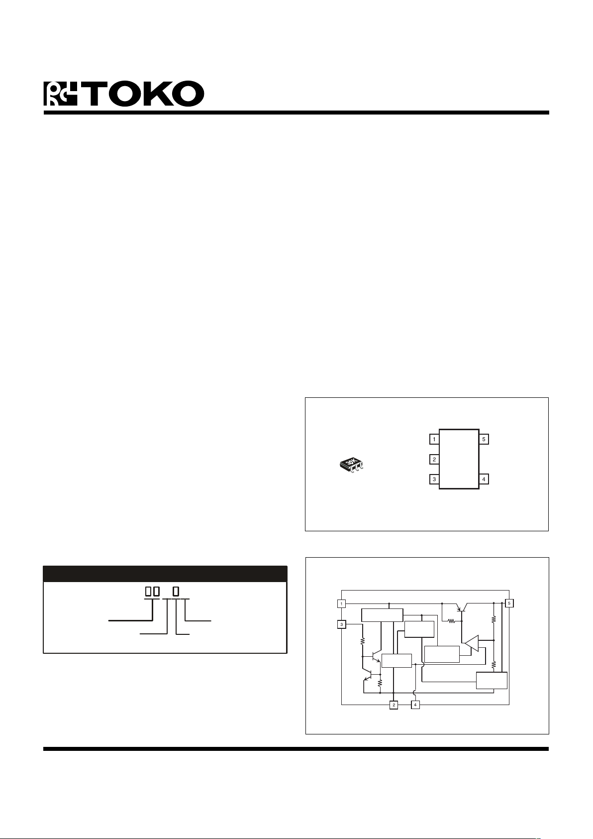
BLOCK DIAGRAM
TK717xxS
LOW DROPOUT VOLTAGE REGULATOR
FEATURES
APPLICATIONS
n Battery Powered Systems
n Measurement Systems
n Mobile Communications Systems
n Cordless Phone, PHS, GSM, CDMA
n Industrial Equipment
n Personal Computers, Barcode Readers
DESCRIPTION
TK717xxS is a low dropout linear regulator with a built-in
electronic switch. The internal switch can be controlled by
TTL or CMOS logic levels. The device is in the ON state
when the control pin is pulled to a logic high level. In the OFF
state, the output impedance becomes very low, quickly
discharging the output capacitor. An external capacitor can
be connected to the noise bypass pin to lower the output
noise level to 30 ~ 50 mV
RMS
. An internal PNP pass transistor
is included to achieve a low dropout voltage of 103 mV at
100 mA load current. The TK717xx has an exceptionally
low quiescent current of 72 mA at no load and 0.8 mA with
a 50 mA load. The standby current is typically 100 pA. The
circuit features very good stability. The ripple rejection is 90
dB at 400 Hz and 80 dB at 1 kHz. Stable operation is
achieved with an output capacitor as low as 0.22 mF; a
capacitor of any type may be used. (However, the larger the
output capacitor is, the better the overall characteristics will
be.)
The TK717xxS is available in a very small SOT23-5 surface
mount package.
CONTROL
GND
V
IN
+
-
BANDGAP
REFERENCE
THERMAL &
OVER CURRENT
PROTECTION
NOISE
BYPASS
CONTROL CIRCUIT
CONSTANT
CURRENT
SOURCE
V
OUT
AUTO
DISCHARGE
CIRCUIT
GND
V
IN
NOISE
BYPASS
V
OUT
CONTROL
TK717 S L
Voltage Code
ORDERING INFORMATION
Package Code
PACKAGE CODE
S: SOT23-5
VOLTAGE CODE
24 =2.4 V
25 =2.5 V
26 =2.6 V
27 =2.7 V
28 =2.8 V
29 =2.9 V
30 =3.0 V
31 =3.1 V
32 =3.2 V
33 = 3.3 V
34 = 3.4 V
35 = 3.5 V
36 = 3.6 V
37 = 3.7 V
38 = 3.8 V
39 = 3.9 V
40 = 4.0 V
41 = 4.1 V
15 = 1.5 V
16 = 1.6 V
17 = 1.7 V
18 = 1.8 V
19 = 1.9 V
20 = 2.0 V
21 = 2.1 V
22 = 2.2 V
23 = 2.3 V
42 = 4.2 V
43 = 4.3 V
44 = 4.4 V
45 = 4.5 V
46 = 4.6 V
47 = 4.7 V
48 = 4.8 V
49 = 4.9 V
50 = 5.0 V
Operating Temp. Range
Tape/Reel Code
OPERATING TEMP. RANGE
C: -30 ~ 80°C
TAPE/REEL CODE
L: Tape Left
0
1
S

Page 2 October 2001 TOKO, Inc.
TK717xxS
ABSOLUTE MAXIMUM RATINGS
Supply Voltage............................................... -0.4 to16 V
Power Dissipation (Note 1) ................................. 500 mW
Reverse Bias Voltage ..................................... -0.4 to 6 V
Operating Voltage Range ............................... 1.8 to 14 V
Storage Temperature Range .....................-55 to +150 °C
Operating Temperature Range..................... -30 to +80 °C
Noise Bypass Pin Voltage .............................. -0.4 to 5 V
Control Pin Voltage ....................................... -0.4 to 16 V
Short Circuit Current............................................ 410 mA
TK717xxSCL ELECTRICAL CHARACTERISTICS
Test conditions: TA = 25 °C, unless otherwise specified.
LOBMYSRETEMARAPSNOITIDNOCTSETNIMPYTXAMSTINU
V
TUO
egatloVtuptuO 1elbaTeeS
geReniLnoitalugeReniL
VNIV=
)PYT(TUO
VotV1+
)PYT(TUO
,V6+ D V5=V
3.05 Vm
geRdaoLnoitalugeRdaoL
I<Am5
TUO
2etoN,Am001<842Vm
I<Am5
TUO
2etoN,Am002<7216Vm
V
PORD
egatloVtuoporD
)5etoN(
I
TUO
Am05=56031Vm
I
TUO
Am001=301002Vm
I
TUO
V4.2(Am002= £ V
TUO
)361003Vm
I
TUO
V1.2(Am081= £ V
TUO
)V4.2<361003Vm
I
)XAM(TUO
tnerruCtuptuOmumixaMVnehW
TUO
2etoN,V3.0nwoD082073Am
V8.1 £ V
NI
£ eulaVecnerefeR,V1.2052Am
I
Q
tnerruCtnecseiuQI
TUO
IgnidulcxEAm0=
TNOC
27011
mA
I
YBTS
tnerruCybdnatSV
CC
V,V8=
TNOC
£ edoMffO,V51.00.01.0
mA
I
DNG
tnerruCniPDNGI
TUO
Am05=8.05.1Am
I
sid
tnerruCegrahcsiDV
VER
)02717(edoMffO,V2=3192Am
V
VER
)03717(edoMffO,V3=3283Am
V
VER
)04717(edoMffO,V4=5214Am
V
VER
)05717(edoMffO,V5=7244Am

October 2001 TOKO, Inc. Page 3
TK717xxS
LOBMYSRETEMARAPSNOITIDNOCTSETNIMPYTXAMSTINU
)4dna3etoNeeS(SNOITACIFICEPSLANIMRETLORTNOC
I
TNOC
tnerruClortnoCV
TUO
etatSnOV8.1=68.05.2Aµ
V
)NO(TNOC
NOegatloVlortnoCedoMnO6.1V
V
)FFO(TNOC
FFOegatloVlortnoCedoMffO6.0V
V
FER
lanimreTssapyBesioN
egatloV
62.1V
DV
TUO
/DT
tneiciffeoCerutarepmeT C°/mpp52=pyTeulaVecnerefeR
V
ON
esioNtuptuO02.0eulaVecnerefeR m /V Ö zHk1talacipyTzH
TK717xxSCL ELECTRICAL CHARACTERISTICS (CONT.)
Test conditions: TA = 25 °C, unless otherwise specified.
Note 1: Power dissipation is 150 mW in free air. Power dissipation is 500 mW when mounted as recommended. Derate at 4.0 mW/°C for operation
above 25°C.
Note 2: This value depends on the output voltage. This is a reference value for a 3 V output device.
Note 3: The input current decreases to the pA level by connecting the control terminal to GND.
Note 4: The pull-down resistor is not built-in.
Note 5: The minimum operating voltage for VIN can be 1.8 V. Also, the minimum voltage required for VIN is VIN = V
DROP
+ V
OUT
. As a result, operating
at V
OUT
£ 2.0 V at the mimimum input operating voltage is not preferred.
General Note: The operation of -30 °C to 80 °C is guaranteed by design (verified by sample inspection).
General Note: Exceeding the “Absolute Maximum Rating “may damage the device.
General Note: Output noise is 0.20 mV/ ÖHz typical at 1 kHz: BW 400 to 30 kHz and 30 ~ 60 m Vrms.
General Note: Connecting a capacitor to the noise by pass pin will decrease the output noise voltage.

Page 4 October 2001 TOKO, Inc.
TK717xxS
TUPTUO
EGATLOV
EGATLOV
EDOCV
TUO
NIMV
TUO
XAM
TSET
EGATLOV
TUPTUO
EGATLOV
EGATLOV
EDOCV
TUO
NIM
V
TUO
XAM
TSET
EGATLOV
V5.151V054.1V055.1V5.2V3.333V052.3V053.3V3.4
V6.161V055.1V056.1V6.2V4.343V943.3V154.3V4.4
V7.171V056.1V057.1V7.2V5.353V744.3V355.3V5.4
V8.181V057.1V058.1V8.2V6.363V645.3V456.3V6.4
V9.191V058.1V059.1V9.2V7.373V446.3V657.3V7.4
V0.202V059.1V050.2V0.3V8.383V347.3V758.3V8.4
V1.212V050.2V051.2V1.3V9.393V148.3V959.3V9.4
V2.222V051.2V052.2V2.3V0.404V049.3V060.4V0.5
V3.232V052.2V053.2V3.3V1.414V830.4V261.4V1.5
V4.242V053.2V054.2V4.3V2.424V731.4V362.4V2.5
V5.252V054.2V055.2V5.3V3.434V532.4V563.4V3.5
V6.262V055.2V056.2V6.3V4.444V433.4V664.4V4.5
V7.272V056.2V057.2V7.3V5.454V234.4V865.4V5.5
V8.282V057.2V058.2V8.3V6.464V135.4V966.4V6.5
V9.292V058.2V059.2V9.3V7.474V926.4V177.4V7.5
V0.303V059.2V050.3V0.4V8.484V827.4V278.4V8.5
V1.313V050.3V051.3V1.4V9.494V628.4V479.4V9.5
V2.323V051.3V052.3V2.4V0.505V529.4V570.5V0.6
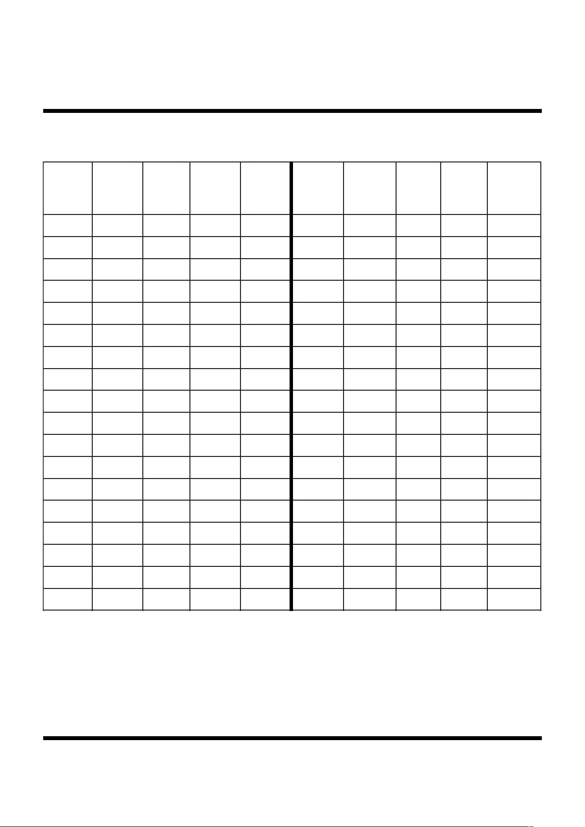
TK717xxSCL ELECTRICAL CHARACTERISTICS TABLE 1
Test Conditions: VIN = V
OUT(TYP)
+ 1 V, I
OUT
= 5 mA, TA = 25 °C, unless otherwise specified.
The output voltage table indicates the standard value when manufactured.
 Loading...