TK70403
20P
1.03 V REGULATOR WITH ON/OFF SWITCH
FEATURES
■ Low Input Voltage Operation (Single Battery Cell)
■ Internal PNP Transistor
■ Internal Shutdown Control (Off Current, 0.1 µA max)
■ Low Dropout Voltage [30 mV (typ.) at 2 mA]
■ Miniature Package (SOT-26)
■ Very Low Noise
DESCRIPTION
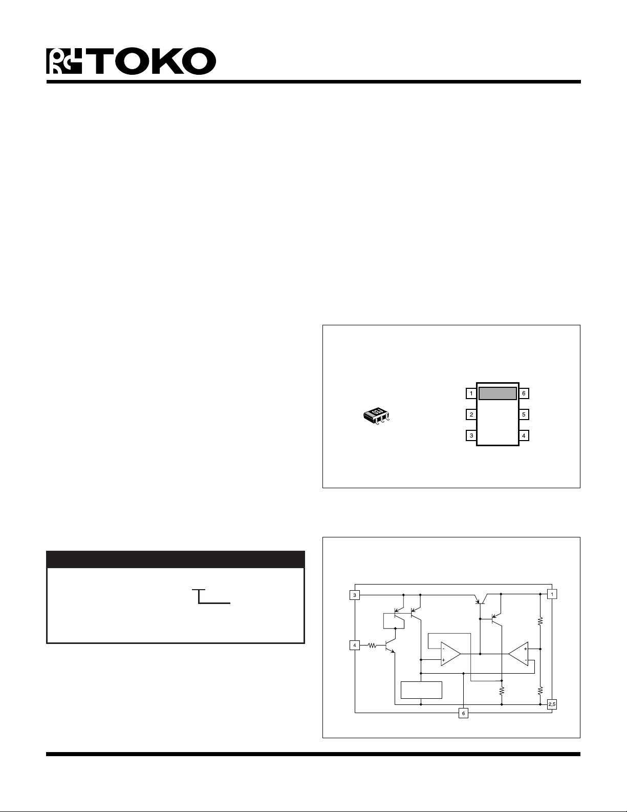
TK70403 is a low dropout, linear regulator with a built-in
electronic switch. A pin for a bypass capacitor is provided,
which connects to the internal circuitry to lower the overall
output noise level.
An internal PNP pass-transistor is used in order to achieve
low dropout voltage (typically 30 mV at 2 mA load current).
This makes it possible to maintain a stable output voltage
as the battery voltage decreases, extending the useful
battery life.
APPLICATIONS
■ Pagers
■ Personal Communication Equipment
■ Portable Consumer Equipment
■ Radio Control Systems
■ Single Battery Cell Systems
TK70403
V
OUT
GND
V
IN
NOISE
BYPASS
GND
CONTROL
The TK70403 is available in a miniature SOT-26 surface
mount package.
ORDERING INFORMATION
TK70403MTB
Tape/Reel Code
TAPE/REEL CODE
TB: Tape Left
V
CONTROL
BLOCK DIAGRAM
IN
BANDGAP
REFERENCE
NOISE
BYPASS
V
GND
OUT
January 1999 TOKO, Inc. Page 1

TK70403
ABSOLUTE MAXIMUM RATINGS
Supply Voltage ........................................................... 6 V
Power Dissipation (Note 1) ................................ 350 mW
Junction Temperature ........................................... 150 °C
Storage Temperature Range ................... -55 to +150 °C
TK70403 ELECTRICAL CHARACTERISTICS
Test Conditions: VIN = 1.4 V, TA = 25 °C, R
LOBMYSRETEMARAPSNOITIDNOCTSETNIMPYTXAMSTINU
= 820 KΩ, unless otherwise specified.
CONT
Operating Temperature Range ...................-10 to +60 °C
Operating Voltage Range.............................. 0.9 to 5.0 V
Lead Soldering Temperature (10 s) ...................... 235 °C
I
YBTS
V
TUO
V
PORD
I
TUO
I
Q
geReniLnoitalugeReniLV
geRdaoLnoitalugeRdaoLI
/∆T
∆V
TUO
V
fer
I
TNOC
V
V
Note 1: Power dissipation is 350 mW when mounted as recommended. Derate at 2.8 mW/°C for operation above 25 °C.
Note 2: I
Gen Note: Ripple rejection and noise voltage are affected by the value and characteristics of the capacitor used. Example: Ripple rejection is 48
Gen Note: Parameters with min. or max. values are 100% tested at TA = 25 °C.
)NO(TNOC
)FFO(TNOC
when V
OUT
dB at CL = 1 µF, CN = 0.1 µF, I
drops 0.4 V from V
OUT
tnerruCybdnatSV
egatloVtuptuOI
egatloVtuoporDI
NI
TUO
TUO
Am2=89.030.1560.1V
Am2=60.0V
tnerruCtuptuO)2etoN(0105Am
tnerruCtnecseiuQI
tneiciffeoCerutarepmeTI
TUO
NI
TUO
TUO
Am2=52.0C°/Vm
egatloVecnerefeR4.0V
R:SNOITACIFICEPSLANIMRETLORTNOC
TNOC
tnerruClanimreTlortnoCV
K028= ΩΩΩΩΩ
TNOC
)NO(egatloVlortnoCNOtuptuO58.0V
)FFO(egatloVlortnoCFFOtuptuO03.0V
.
OUT(TYP)
= 2 mA, f = 400 Hz.
OUT
FFOtuptuO,V4.1=1.0Aµ
IgnidulcxE,Am0=
TNOC
051Aµ
V7.1ot34.1=02Vm
Am0.5ot1.0=02Vm
NOtuptuO,V0.1=0.1Aµ
Page 2 January 1999 TOKO, Inc.

TK70403
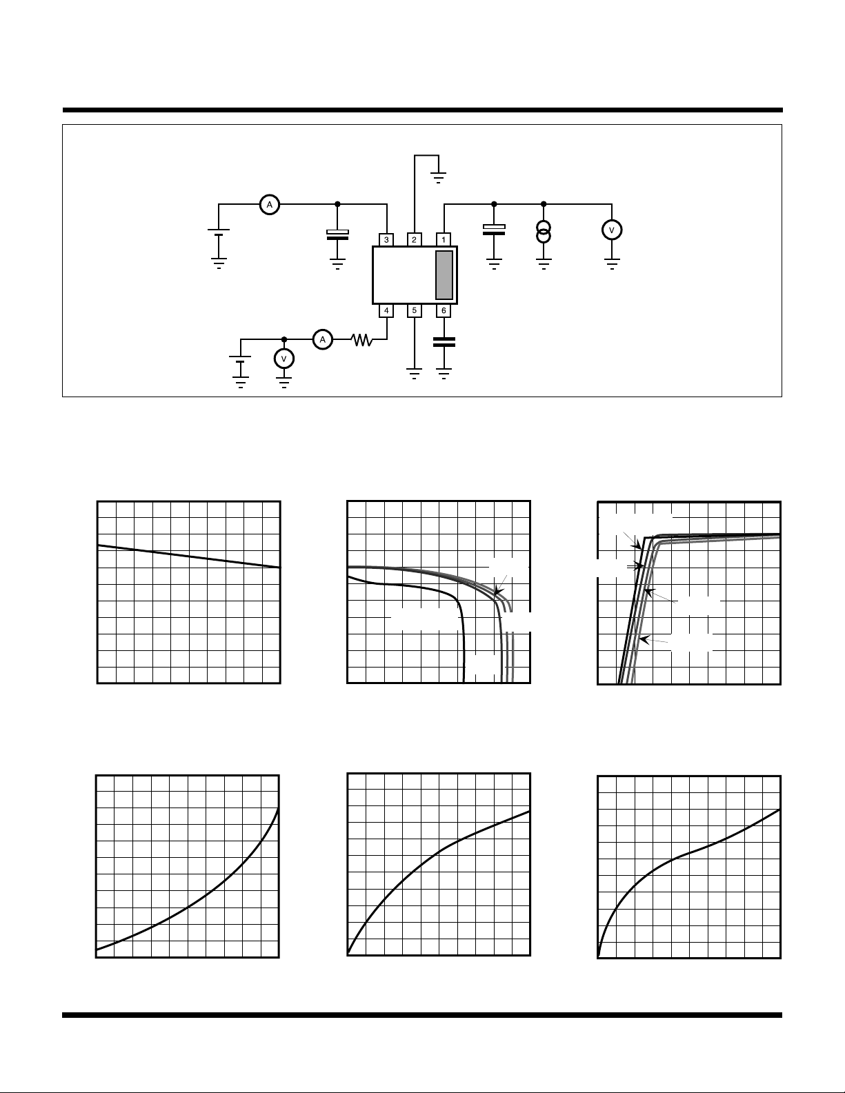
TEST CIRCUIT
I
IN
V
IN
GND
V
OUT
1 µF
V
IN
1 µF
I
OUT
V
OUT
V
CONT
TYPICAL PERFORMANCE CHARACTERISTICS
OUTPUT VOLTAGE VS.
OUTPUT CURRENT
1.05
1.04
(V)
1.03
OUT
V
1.02
1.01
0 5 10
I
(mA)
OUT
I
CONT
CONT
R
CONT
820 kΩ
GND
NOISE
BYPASS
C
N
0.1 µF
TA = 25 °C, unless otherwise specified.
OUTPUT VOLTAGE
OUTPUT CURRENT
1.5
1.2
(V)
0.9
OUT
V
0.6
VIN = 1.1 V
0.3
0
0 50 100
I
(mA)
OUT
VS.
1.4 V
1.6 V
1.2 V
OUTPUT VOLTAGE
INPUT VOLTAGE
1.08
I
= 0 mA
OUT
1.04
2.5 mA
(V)
1.00
OUT
V
0.96
0.92
5.0 mA
7.5 mA
0.8 1.0 1.2 1.4 1.6 1.8
VIN (V)
VS.
GROUND CURRENT VS.
OUTPUT CURRENT
2.5
2.0
1.5
(mA)
GND
I
1.0
0.5
0
0 10 20 30 40 50
I
(mA)
OUT
DROPOUT VOLTAGE
OUTPUT CURRENT
100
80
(mV)
60
DROP
40
V
20
0
0 2 4 6 8 10
I
(mA)
OUT
VS.
DROPOUT VOLTAGE VS.
OUTPUT CURRENT
200
(mV)
100
DROP
V
0
0 10 20 30 40 50
I
(mA)
OUT
January 1999 TOKO, Inc. Page 3
 Loading...