TOKO TK70002MCB Datasheet

TK70002
20P
SINGLE INPUT, TWO OUTPUT SOLID STATE SWITCH
FEATURES
■ Internal PNP Power Transistor
■ Reverse Bias Voltage Protection
■ Very Low Input-Output Voltage Difference
■ Very Low Standby Current
■ Overtemperature Protection
■ Single Input with Two Controlled Outputs
■ Active High On/Off Control
DESCRIPTION
The TK70002 is a monolithic bipolar integrated circuit with
high side current switches of low saturation type. The
supply current, including the control current, is virtually
zero (pA level) when the control pin is “off”. The impedance
on the output side is high and the reverse current does not
flow when the control pin is “off.” These are effective to
decrease the dissipation currents, making the TK70002 a
very efficient device for power management and power
distribution control.
APPLICATIONS
■ Battery Powered Systems
■ Radio Control Systems
■ Automatic Test Equipment (ATE)
■ Power Management
■ Process Control Equipment
■ Power Distribution Control
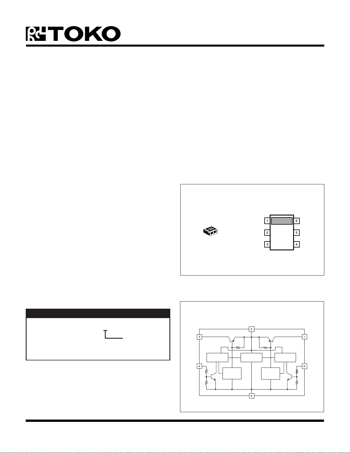
TK70002
OUTPUT 1
INPUT
OUTPUT 2
CONT 1
GND
CONT 2
The TK70002 is available in a miniature SOT-23-6 surface
mount package. When mounted as recommended, this
package is capable of dissipating up to 350mW.
ORDERING INFORMATION
TK70002MCB
Tape/Reel Code
TAPE/REEL CODE
B: Tape Left
OUTPUT 2
CONT 2
BLOCK DIAGRAM
SW
CIRCUIT
BASE
CONTROL
CURRENT
INPUT
THERMAL
PROTECTION
GND
BASE
CONTROL
CURRENT
SW
CIRCUIT
OUTPUT 1
CONT 1
January 1999 TOKO, Inc. Page 1

TK70002
ABSOLUTE MAXIMUM RATINGS
Supply Voltage ......................................................... 14 V
Output Current .................................................... 130 mA
Power Dissipation (Note 1) ................................ 350 mW
Control Terminal Voltage ........................................... 8 V
Reverse Bias Voltage................................................. 8 V
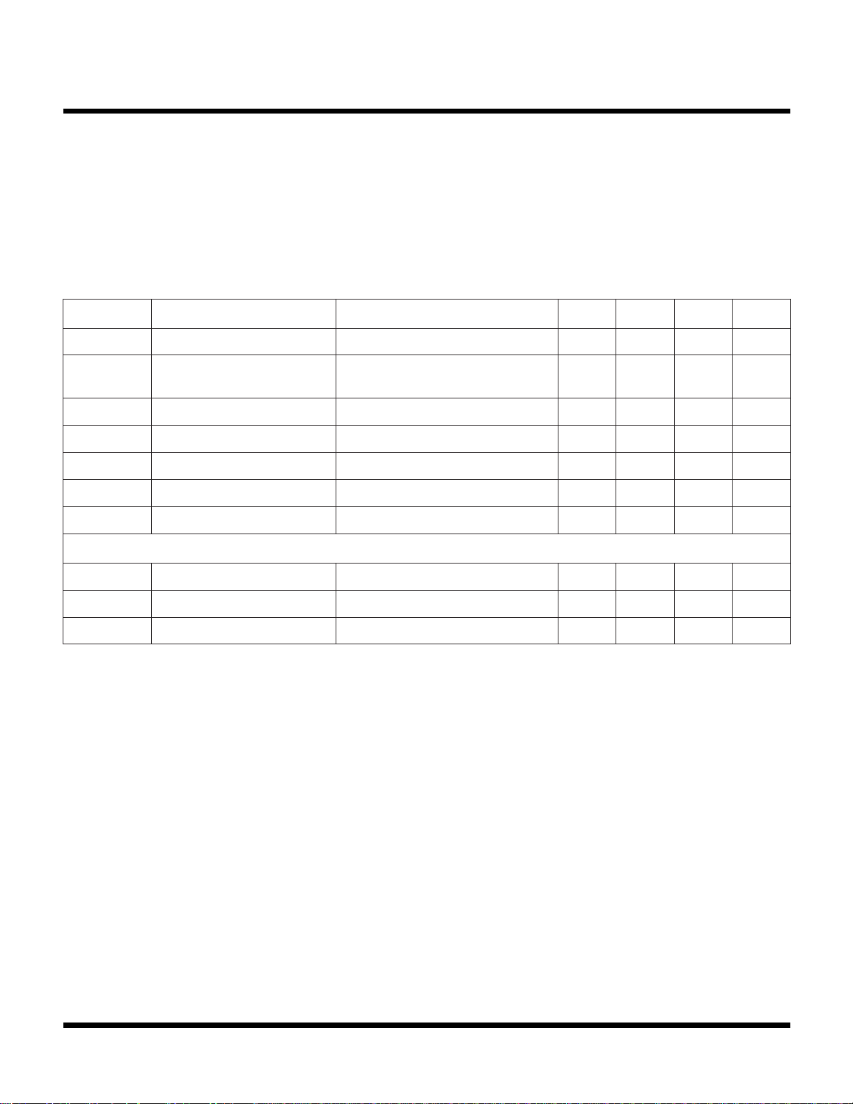
TK70002 ELECTRICAL CHARACTERISTICS
Test conditions: VIN = 2.5 V, T
LOBMYSRETEMARAPSNOITIDNOCTSETNIMPYTXAMSTINU
= 25 °C, unless otherwise specified.
A
Storage Temperature Range ................... -55 to +150 °C
Operating Temperature Range ...................-30 to +80 °C
Operating Voltage Range............................... 1.6 to 12 V
Lead Soldering Temperature (10 s) ..................... 235 °C
I
Q
I
I
I
V
∆V
I
YBTS
TUO
DNG
PORD
D
VER
tnerruCtnecseiuQI
tnerruCybdnatS
tnerruCtuptuOV
)3etoN(tnerruCdnuorGI
egatloVtuoporDI
tnerruCsaiBesreveRV
TUO
V
NI
V
TUO
TUO
slennahCneewteBecnalaBV
NI
V0=
TNOC
PORD
V5.0=07011Am
Am05=5.25.4Am
Am05=81.053.0V
PORD
V,V0=
VER
IedulcxE,Am0=
TNOC
,FFOtuptuO,V8=
I,ecnereffid
TUO
V,V8=
TNOC
52.056.0Am
5.0001An
Am05=152Vm
V0=3.005An
LANIMRETLORTNOCFFO/NO
I
TNOC
V
V
Note 1: Power dissipation is 350 mW when mounted as recommended. Derate at 2.8 mW/°C for operation above 25 °C. Power dissipation is
Note 2: By grounding this terminal, the operation completely stops and the input current decreases to a pA level.
Note 3: Ground current is defined as IIN - I
Gen. Note: Parameters with min. or max. values are 100% tested.
Gen. Note: Exceeding the “Absolute Maximum Ratings” can damage the device.
)NO(TNOC
)FFO(TNOC
150 mW in Free Air. Derate at 1.2 mW/°C for operation above 25 °C.
tnerruClanimreTlortnoCV
TNOC
V6.1=751Aµ
)NO(egatloVlortnoCNOtuptuO2.1V
)FFO(egatloVlortnoC)2etoN(FFOtuptuO3.0V
, excluding control current. Refer to “Definition of Terms.”
OUT
Page 2 January 1999 TOKO, Inc.

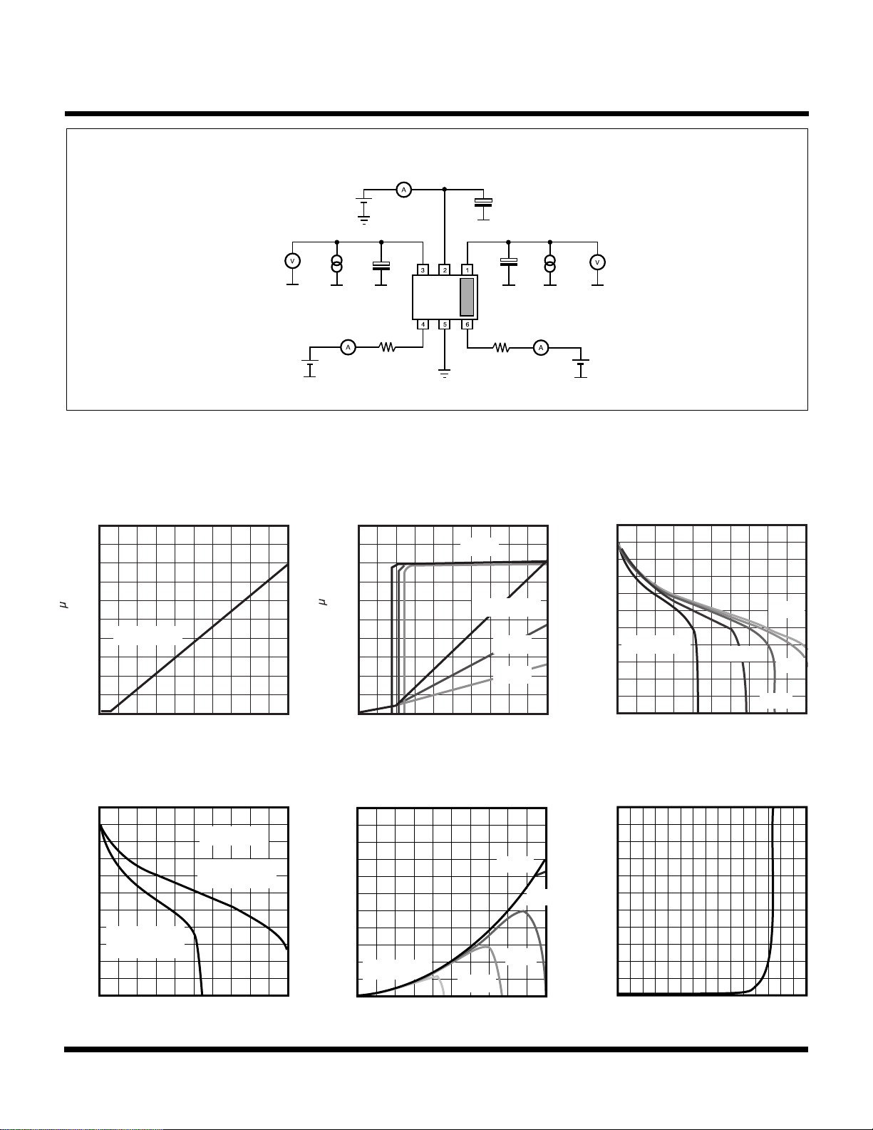
TEST CIRCUIT
V
(
V)
I
(
A)
I
(
A)
INPUT
C
V
OUT 2
V
CONT 2
V
I
I
CONT 2
IN
OUT 2
C
L 2
OUTPUT 2
= 0.1 µF
R
CONT 2
I
IN
OUTPUT 1
C
CONT 1CONT 2
R
IN
0.1 µF
= 0.1 µF
L 1
CONT 1
I
CONT 1
I
OUT 1
V
CONT 1
V
OUT 1
TYPICAL PERFORMANCE CHARACTERISTICS
TK70002
CONTROL CURRENT 1
CONTROL VOLTAGE
100
80
60
( A)
R
= 0
40
CONT
I
CONT
20
0
0 2 4 6 8 10
V
(V)
CONT
DROPOUT VOLTAGE VS.
OUTPUT CURRENT
-100
m
-200
DROP
-300
0
SINGLE
VIN = 2.5 V
PARALLEL
OPERATION
OPERATION
-400
0 100 200
I
(mA)
OUT
VS.
CONTROL CURRENT 2
CONTROL VOLTAGE
V
OUT
40
30
( A)
20
CONT
I
R
10
0
0 1 2 3 4 5
V
(V)
CONT
GROUND CURRENT
OUTPUT CURRENT
10
m
5
GND
VIN = 1.0 V
1.2 V
0
0 50 100
I
(mA)
OUT
CONT
100 k
200 k
VS.
1.8 V
VS.
= 0
1.4 V
1.6 V
DROPOUT VOLTAGE
OUTPUT CURRENT
0
-100
(mV)
-200
DROP
VIN = 1.0 V
-300
V
1.2 V
-400
0 50 100
I
(mA)
OUT
REVERSE CURRENT
REVERSE VOLTAGE
2
n
1
REV
0
0 5 10 15
V
(V)
REV
VS.
1.8V
1.6 V
1.4 V
VS.
January 1999 TOKO, Inc. Page 3
 Loading...