TOKO TK65433MTL, TK65430MTL, TK65425MTL, TK65427MTL, TK65424MTL Datasheet
...
ADVANCED INFORMATION
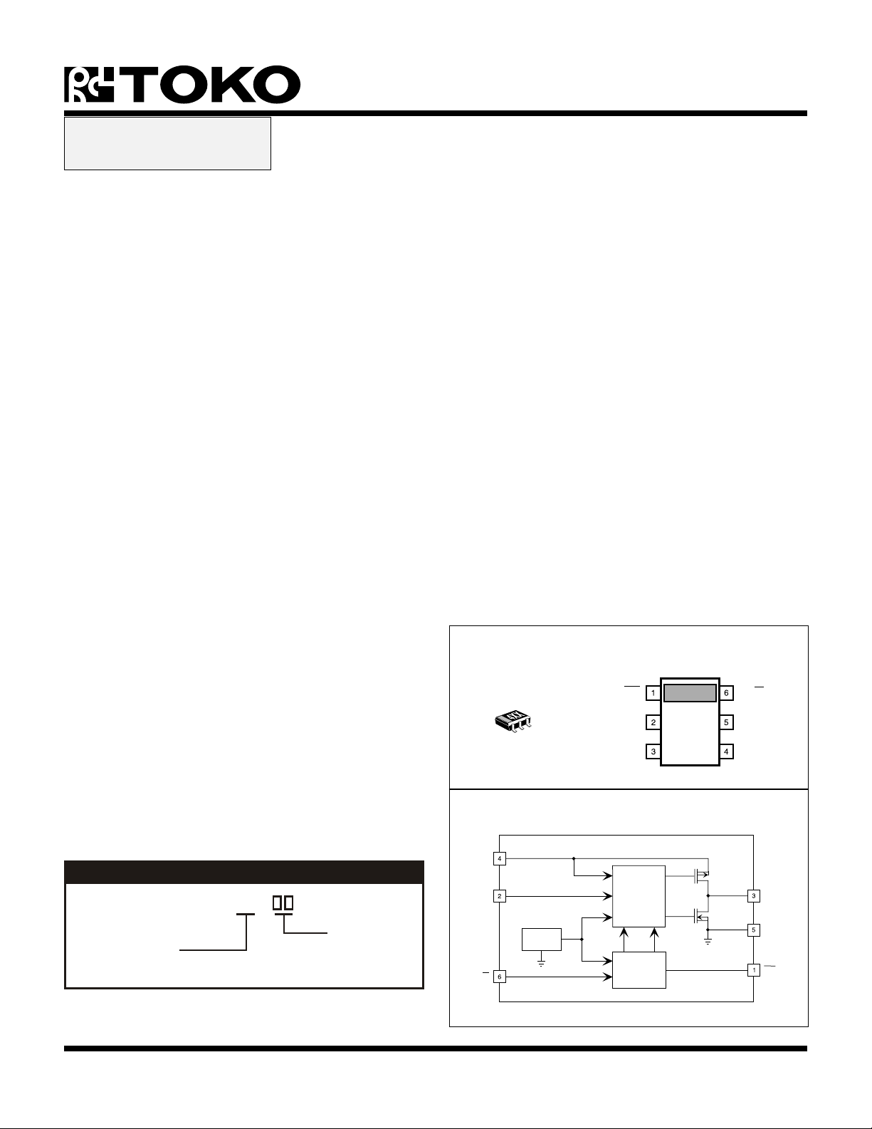
V
OUT
LBO
V
IN
SW
GND
LBI/SB
TK654xx
ADVANCED
STEP-DOWN CONVERTER WITH BATTERY MONITOR
INFORMATION
FEATURES
■ Minimum External Component Count (1 coil, 1 cap)
■ Miniature 6 Pin SOT23L-6 Surface Mount Package
■ Up To 95% Efficient
■ Extremely Low Operating Current (24 µA)
■ Low Quiescent Current (18 µA)
■ Low Ripple
■ Fast Transient Response
■ Linear Dropout Characteristics
■ Short Circuit Protection
■ Regulates Down to 1.8 V
■ Synchronous Rectification
■ Internal Battery Monitor
DESCRIPTION
The TK654xx low power step-down converter is designed
for portable battery systems, capable of operating from a
single Li-ion battery cell or multiple alkaline or rechargeable
(NiCd or NiMH) battery cells (up to 6 V). The TK654xx
provides the power switch, synchronous rectifier, and the
control circuit for a buck step-down converter. Only two
external components are required to complete the stepdown conversion.
APPLICATIONS
■ Battery Powered Systems
■ Cellular Telephones
■ Pagers
■ Personal Communications Equipment
■ Radio Controlled Systems
■ Toys
Driving the SB pin low will disable the TK654xx and drop
the quiescent current on the input supply to approximately
18 µA.
Pulse Current Amplitude control is used to regulate the
voltage at the V
of the TK654xx drops below the regulation threshold, a
current pulse is transferred from the input supply to the
output. The TK654xx utilizes a proprietary control scheme,
where the average amplitude of the current pulse is varied
depending upon the current loads. The proprietary
architecture allows fast transient response and minimal
ripple while maintaining ease-of-use and low component
count.
The TK654xx is available in a miniature 6-pin SOT23L-6
surface mount package.
pin of the IC. When the output voltage
OUT
TK654xxM
The TK654xx provides laser-trimmed output voltages
ranging from 1.8 V to 3.3 V. The low resistance MOSFET
switch and synchronous rectifier allow average currents
up to 200 mA, while maintaining peak efficiencies up to
95%. A low-battery threshold and turn-off threshold can
be individually programmed by the user, utilizing a single
resistor divider connected to the Low Battery Input (LBI)
pin. When the resistively-divided supply voltage on the
LBI pin drops below approximately 1.22 V, the Low Battery
BLOCK DIAGRAM
Output (LBO) pin will become asserted. The dual-function
LBI pin can alternatively be used as a Standby (SB) pin.
V
IN
ORDERING INFORMATION
V
OUT
REF
LBI/SB
Voltage Code
VOLTAGE CODE
18 = 1.8 V
21 = 2.1 V
24 = 2.4 V
25 = 2.5 V
27 = 2.7 V
30 = 3.0 V
33 = 3.3 V
TK654xxM
Tape/Reel Code
TAPE/REEL CODE
TL: Tape Left
September 1999 TOKO, Inc. Page 1
CONTROL
CIRCUIT
BATTERY
MONITOR
SW
GND
LBOOFF
LBO

TK654xx
ADVANCED INFORMATION
ABSOLUTE MAXIMUM RATINGS
All Pins Except GND ............................................... 6.5 V
Power Dissipation (Note 1) ................................ 400 mW
Storage Temperature Range ................... -55 to +150 °C
Operating Temperature Range ...................-20 to +80 °C
Junction Temperature ...........................................150 °C
Lead Soldering Temperature (10 s.) .....................235 °C
TK654xx ELECTRICAL CHARACTERISTICS
Test conditions: VIN = 5 V, I
LOBMYSRETEMARAPSNOITIDNOCTSETNIMPYTXAMSTINU
= 1 mA, T
OUT
= TJ = Full Operating Temperature Range, unless otherwise specified.
A
V
V
∆V
∆V
I
I
V
V
NI
)GER(TUO
)DAOL(TUO
)ENIL(TUO
)TUOV(Q
)NIV(Q
)IBL(HT
)BS(HT
egatloVtupnI26V
TAT=
egatloVtuptuO
J
)2etoN(C°52=%3-V
GER
%3V
%5-%5+V
noitalugeRdaoLI
noitalugeReniLV
VotnitnerruCtnecseiuQ
VotnitnerruCtnecseiuQ
niP
TUO
niPV
NI
dlohserhTtupnIIBLT
dlohserhTybdnatST
NI
V
AT=J
AT=J
DAOL
V=
TUO
)GER(TUO
)3etoN(
V=
TUO
)GER(TUO
C°52=751.122.1282.1V
C°52=751.122.1282.1V
)3etoN(,Am001ot0=54021Vm
)3etoN(,V6ot4=602Vm
Vm05+
0105Aµ
P
Vm05+5156Aµ
3etoN0An
I
)BS(B
I
)XAM(TUO
I
)CS(TUO
I
)VNOC(Q
I
YBTS
FFEycneiciffEretrevnoC
V
PORD
Note 1: Power dissipation is 400 mW when mounted as recommended. Derate at 3.2 mW/°C for operation above 25 °C. Power dissipation is 200
mW in Free Air. Derate at 1.6 mW/°C for operation above 25 °C
Note 2: V
Note 3: When using test circuit.
Note 4: When using test circuit and ramping VIN down.
Note 5: When using test circuit with SB pin resistors removed and tied to VIN. (VIN = 1.8 V)
Note 6: When using test circuit with SB pin resistors removed and tied to VIN. (VIN = 3.3 V)
= 3.3, 3.0, 2.7, 2.5, 2.4, 2.1, 1.8 V.
REG
tnerruCsaiBtupnIBS
V(ta4etoN
)BS(HT
)Vm001-0040270001An
tnerruCtuptuOmumixaM)3etoN(001Am
tnerruCtiucriCtrohS)3etoN(052Am
tnerruCtnecseiuQretrevnoCI)3etoN(
TUO
Am0=4209Aµ
tnerruCybdnatSretrevnoCnepo1niP,V0=nipBS8156Aµ
I
TUO
TAT=
J
I
TUO
TAT=
J
I
TUO
TAT=
egatloVtuoporD
I
TAT=
J
TUO
J
)3etoN(,Am05=
)81456KT(C°52=
)3etoN(,Am05=
)33456KT(C°52=
)5etoN(,Am05=
)6etoN(,Am05=
6819%
0959%
)81456KT(C°52=
)33456KT(C°52=
001591Vm
57541Vm
Page 2
September 1999 TOKO, Inc.
ADVANCED INFORMATION
TK654xx
1.820
1.815
I
Q(CONV)
V
= 5 V
IN
C
3
10 µF
I
OUT
V
OUT
C
10 µF
1
C
10 µF
+
2
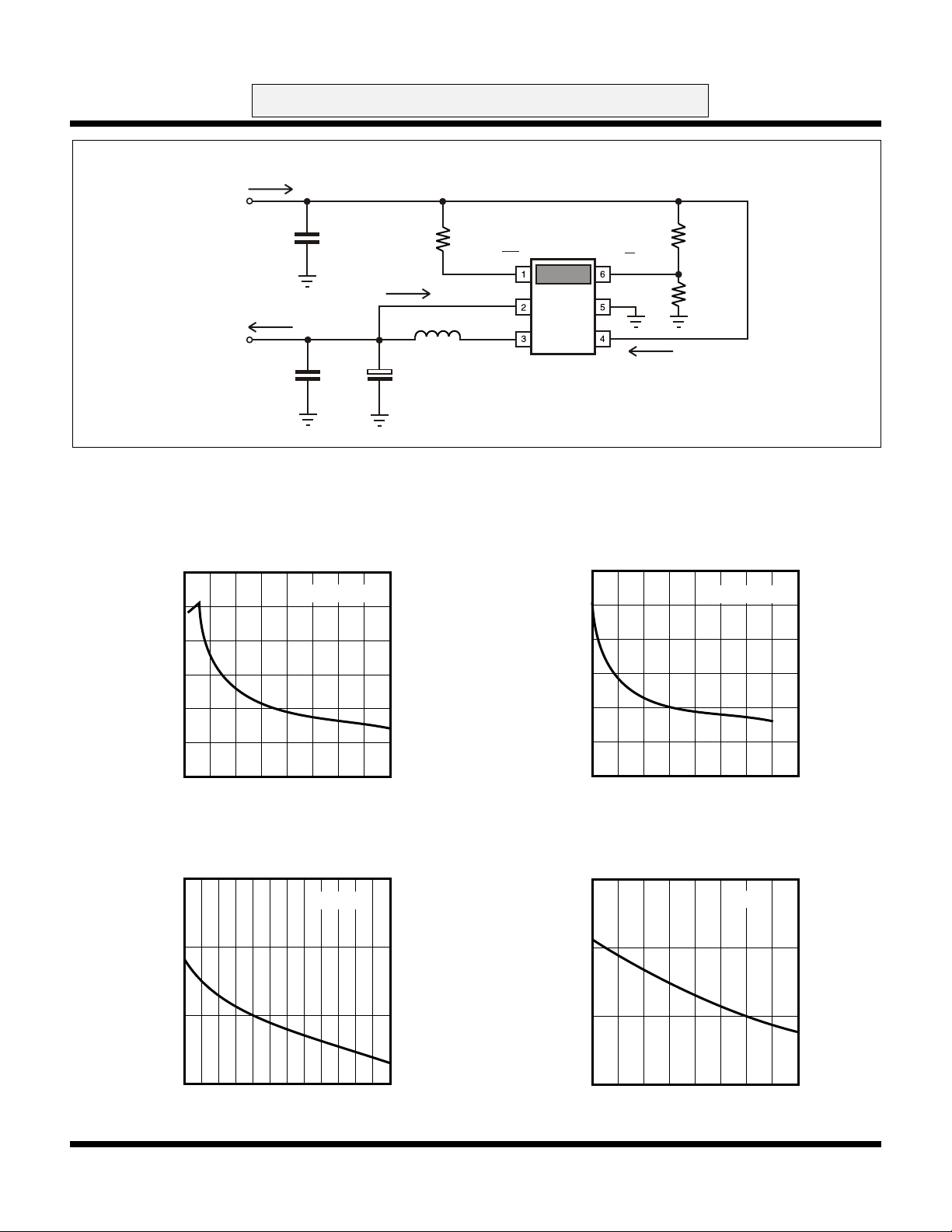
TEST CIRCUIT
R
3
300 K
I
Q(VOUT)
L
1
100 µH
V
LBO
OUT
SW
LBI/SB
GND
V
IN
L
1
C1,C3: Ceramic 10 µF
C2: Tantalum 10 µF
TYPICAL PERFORMANCE CHARACTERISTICS
USING TEST CIRCUIT
TK65418
LINE REGULATION
I
= 1 mA
OUT
3.330
3.325
R
1
634 K
R
2
287 K
I
Q(VIN)
: Toko D10F Coil, PN A814AY-101K
L1:
TK65433
LINE REGULATION
I
= 1 mA
OUT
1.810
(V)
1.805
OUT
V
1.800
1.795
1.790
2.0 2.5 3.0 3.5 4.0 4.5 5.0 5.5 6.0
V
(V)
IN
TK65418
LOAD REGULATION
1.82
VIN = 5 V
1.80
(V)
OUT
V
1.78
1.76
0 20 40 60 80 100 120
I
(mA)
OUT
3.320
(V)
3.315
OUT
V
3.310
3.305
3.300
3.4 3.8 4.2 4.6 5.0 5.4 5.8 6.0
V
(V)
IN
TK65433
3.35
LOAD REGULATION
3.3
(V)
OUT
V
3.25
3.2
0 20 40 60 80 100 120 140 160
I
(mA)
OUT
VIN = 5 V
September 1999 TOKO, Inc. Page 3
TK654xx
ADVANCED INFORMATION
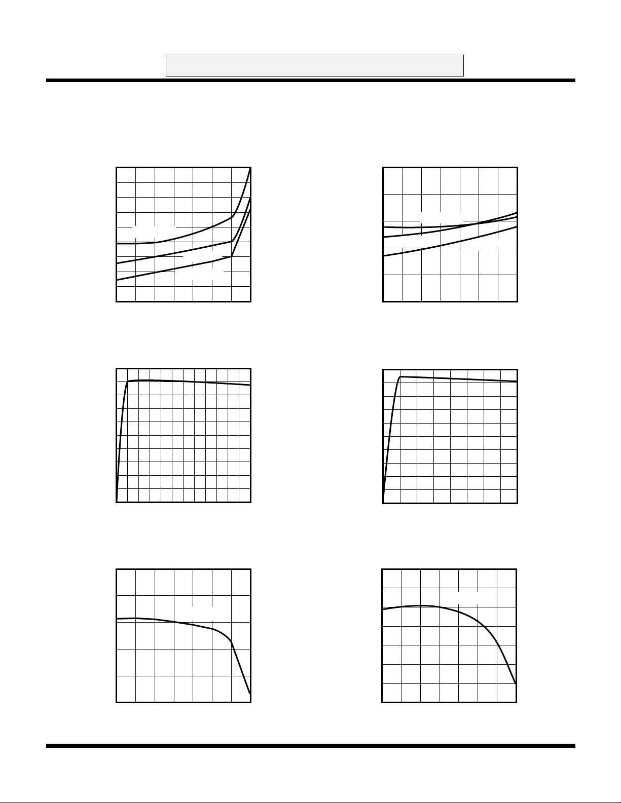
TYPICAL PERFORMANCE CHARACTERISTICS
USING TEST CIRCUIT (CONT.)
LOAD AND TEMPERATURE
TK65418
1.90
REGULATION
1.88
1.86
1.84
(V)
OUT
V
1.82
1.8
1.78
1.76
I
OUT
= 1 mA
I
OUT
I
OUT
= 100 mA
= 50 mA
1.74
1.72
-50 -25 0 25 50 75 100 125
TEMPERATURE (°C)
TK65418
EFFICIENCY vs.
OUTPUT CURRENT
100
90
80
70
60
50
40
30
EFFICIENCY (%)
20
10
0
0 20 40 60 80 100 120
I
(mA)
OUT
LOAD AND TEMPERATURE
TK65433
3.55
REGULATION
3.45
I
= 50 mA
I
OUT
OUT
= 1 mA
(V)
OUT
V
3.35
3.25
3.15
3.05
-50 -25 0 25 50 75 100 125
TEMPERATURE (°C)
TK65433
EFFICIENCY vs.
OUTPUT CURRENT
100
90
80
70
60
50
40
30
EFFICIENCY (%)
20
10
0
0 40 80 120 160
I
(mA)
OUT
I
OUT
= 100 mA
Page 4
EFFICIENCY vs. TEMPERATURE
100
TK65418
95
I
= 50 mA
90
OUT
85
EFFICIENCY (%)
80
75
-50 -25 0 25 50 75 100 125
TEMPERATURE (°C)
EFFICIENCY vs. TEMPERATURE
99
97
95
TK65433
I
OUT
= 50 mA
93
91
EFFICIENCY (%)
89
87
85
-50 -25 0 25 50 75 100 125
TEMPERATURE (°C)
September 1999 TOKO, Inc.
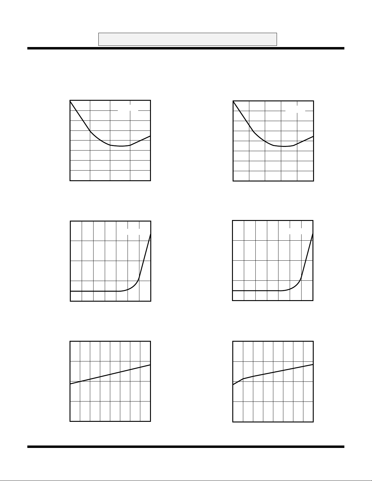
TYPICAL PERFORMANCE CHARACTERISTICS
CONVERTER QUIESCENT
INPUT SUPPLY VOLTAGE
26
25.5
25
24.5
(µA)
24
23.5
Q(CONV)
I
23
22.5
22
2 3 4 5 6
CONVERTER QUIESCENT
200
150
TK65418
CURRENT vs.
VIN (V)
TK65418
CURRENT vs.
TEMPERATURE
ADVANCED INFORMATION
USING TEST CIRCUIT (CONT.)
No Load
No Load
26
25.5
25
24.5
(µA)
24
23.5
Q(CONV)
I
23
22.5
22
3.5 4 4.5 5 5.5 6
200
150
CONVERTER QUIESCENT
INPUT SUPPLY VOLTAGE
CONVERTER QUIESCENT
TK65433
CURRENT vs.
VIN (V)
TK65433
CURRENT vs.
TEMPERATURE
No Load
No Load
TK654xx
(µA)
100
Q(CONV)
I
50
0
-50 -25 0 25 50 75 100 125
TEMPERATURE (°C)
TK65418
STANDBY CURRENT vs.
INPUT SUPPLY VOLTAGE
25
20
(µA)
15
STBY
I
10
5
2 2.5 3 3.5 4 4.5 5 5.5 6
VIN (V)
(µA)
100
Q(CONV)
I
50
0
-50 -25 0 25 50 75 100 125
TEMPERATURE (°C)
STANDBY CURRENT vs.
INPUT SUPPLY VOLTAGE
25
20
(µA)
15
STBY
I
10
5
2 2.5 3 3.5 4 4.5 5 5.5 6
TK65433
VIN (V)
September 1999 TOKO, Inc. Page 5
TK654xx
ADVANCED INFORMATION
TYPICAL PERFORMANCE CHARACTERISTICS (CONT.)
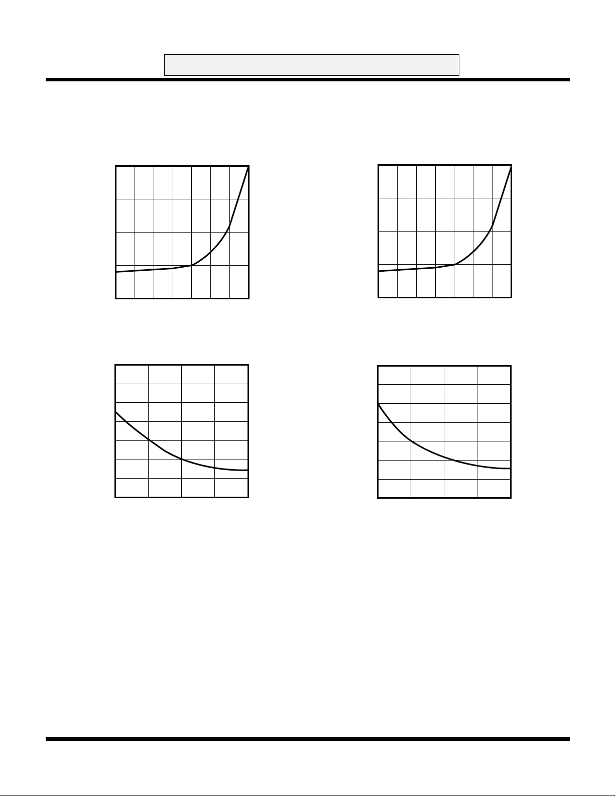
TK65418
STANDBY CURRENT vs.
80
60
(µA)
40
STBY
I
20
0
-50 -25 0 25 50 75 100 125
350
300
250
(mA)
200
TEMPERATURE
TEMPERATURE (°C)
TK65418
MAX OUTPUT CURRENT vs.
INDUCTOR VALUE
STANDBY CURRENT vs.
80
60
(µA)
40
STBY
I
20
0
-50 -25 0 25 50 75 100 125
MAX OUTPUT CURRENT vs.
350
300
250
(mA)
200
TK65433
TEMPERATURE
TEMPERATURE (°C)
TK65433
INDUCTOR VALUE
150
OUT(MAX)
I
100
50
0
60 90 120 150 180
INDUCTOR VALUE (µH)
150
OUT(MAX)
I
100
50
0
60 90 120 150 180
INDUCTOR VALUE (µH)
Page 6
September 1999 TOKO, Inc.
ADVANCED INFORMATION
TYPICAL PERFORMANCE CHARACTERISTICS (CONT.)
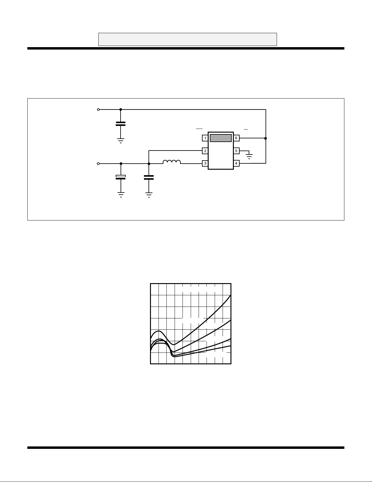
USING RIPPLE TEST CIRCUIT
V
= 5 V
IN
C
3
V
OUT
10 µF
L
1
+
C
2
100 µH
C
1
LBO
OPEN
V
OUT
SW
LBI/SB
GND
V
IN
L1: Toko D10F Coil, PN A814AY-101K
C1 = See Figure Below
C2 = Tantalum 10 µF
C3 = Ceramic 10 µF
TK654xx
PEAK TO PEAK RIPPLE VOLTAGE
RIPPLE vs. OUTPUT CURRENT
70
60
50
40
30
RIPPLE (mV)
20
10
0
0 20 40 60 80 100
C2 = 10 µF Tantalum
C1 = 10 µF
I
OUT
C1 = 20 µF
C1 = 80 µF
(mA)
C1 = 50 µF
September 1999 TOKO, Inc. Page 7
TK654xx
ADVANCED INFORMATION
TYPICAL PERFORMANCE CHARACTERISTICS (CONT.)
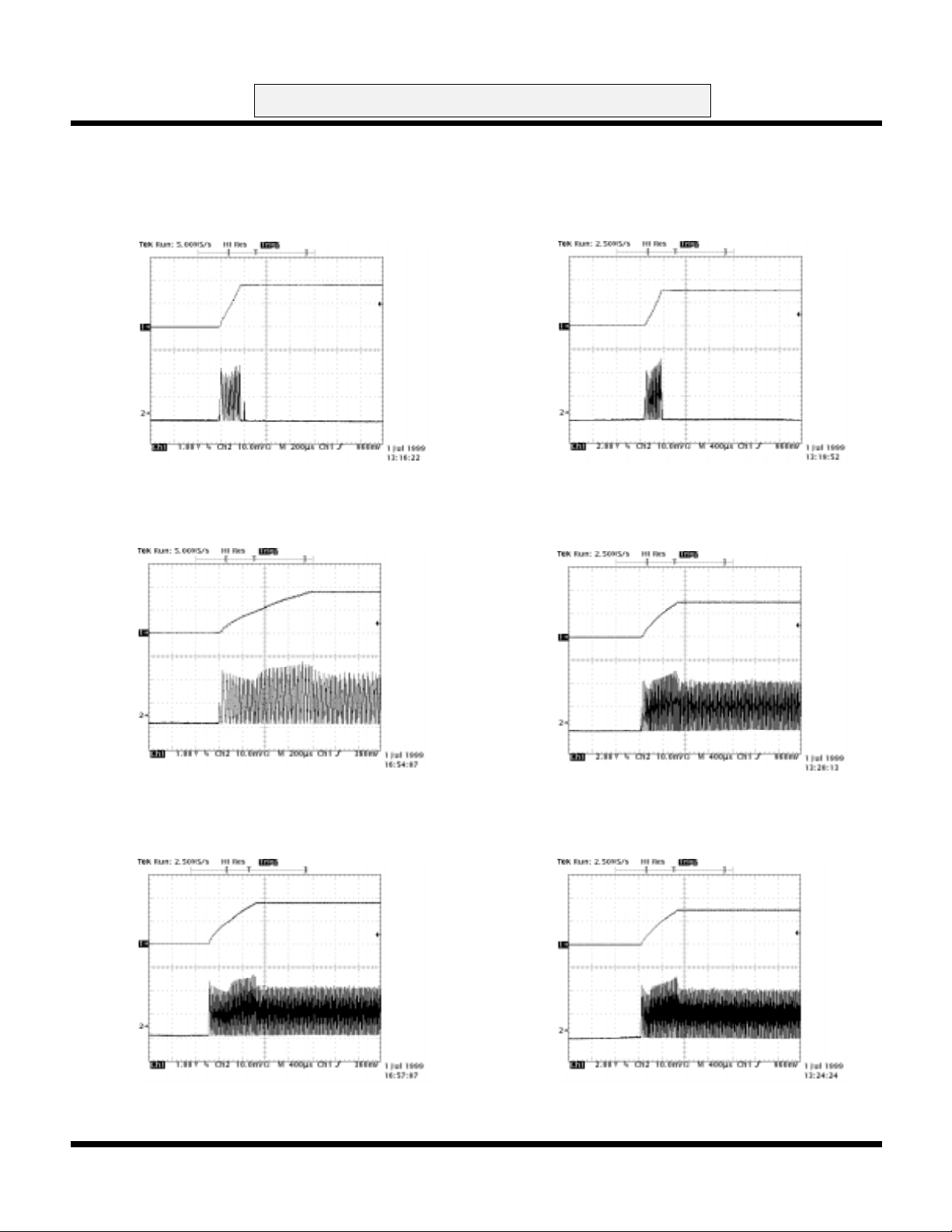
STARTUP TRANSIENT WAVEFORMS
TK65418 - Power Up No Load
TK65418 - Power Up 100mA Load
Output Voltage (1V / div)
Inductor Current (100mA / div)
Output Voltage (1V / div)
1.8V
0.0V
200mA
0mA
1.8V
0.0V
200mA
TK65433 - Power Up No Load
3.3V
Output Voltage (2V / div)
0.0V
200mA
Inductor Current (100mA / div)
0mA
TK65433 - Power Up 100mA Load
3.3V
Output Voltage (2V / div)
0.0V
Inductor Current (100mA / div)
200mA
Page 8
Inductor Current (100mA / div)
TK65418 - Power Up using SB Pin (100mA Load)
Output Voltage (1V / div)
Inductor Current (100mA / div)
0mA
1.8V
0.0V
200mA
0mA
0mA
TK65433 - Power Up using SB Pin (100mA Load)
3.3V
Output Voltage (2V / div)
0.0V
Inductor Current (100mA / div)
200mA
0mA
September 1999 TOKO, Inc.
ADVANCED INFORMATION
TYPICAL PERFORMANCE CHARACTERISTICS (CONT.)
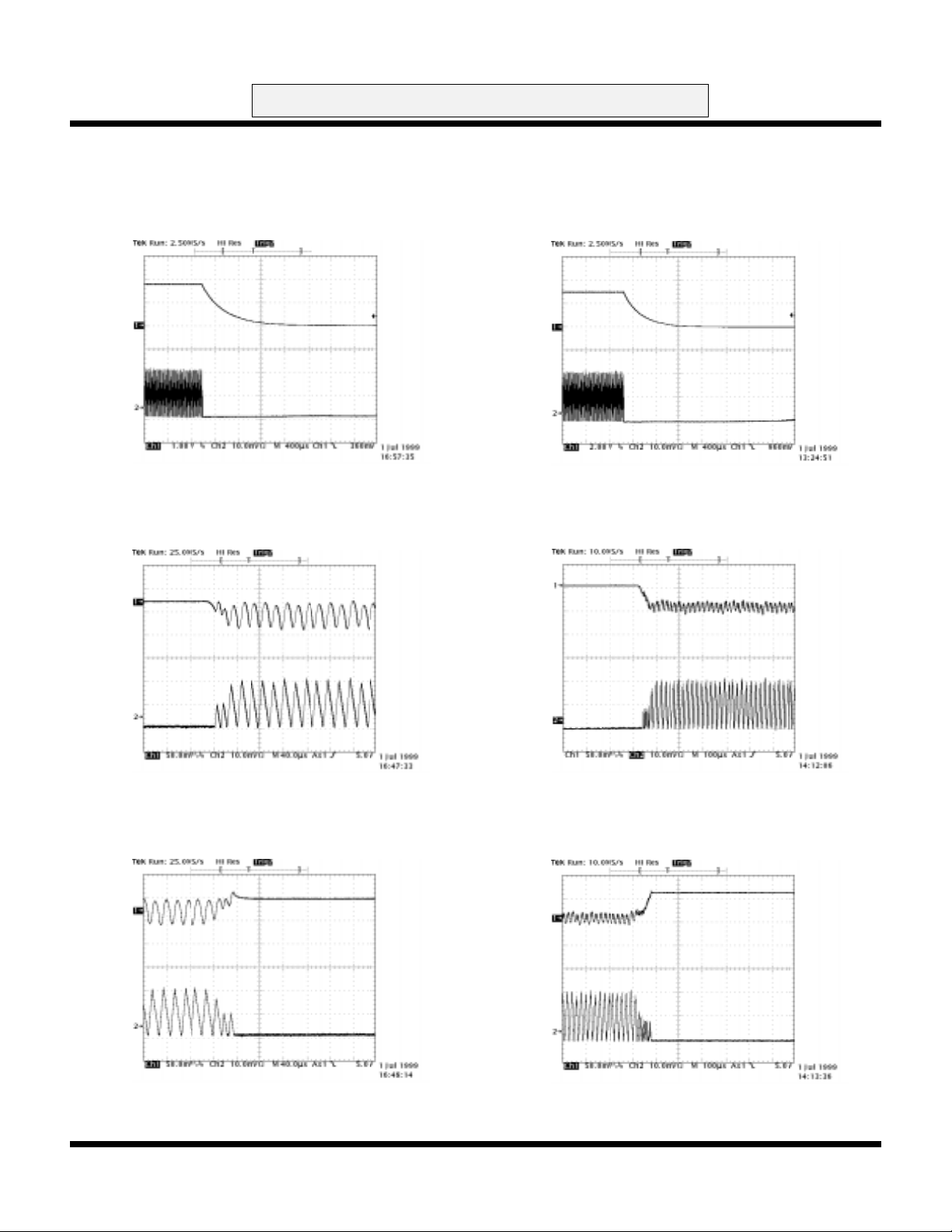
TURN OFF TRANSIENT WAVEFORMS
TK654xx
TK65418 - Power Down using SB Pin (100mA Load)
Output Voltage (1V / div)
Inductor Current (100mA / div)
LOAD TRANSIENT RESPONSE WAVEFORMS
TK65418 - Transient Load (0mA to 100mA Step)
Output Voltage (50mV / div)
Inductor Current (100mA / div)
1.8V
0.0V
200mA
0mA
200mA
TK65433 - Power Down using SB Pin (100mA Load)
3.3V
Output Voltage (2V / div)
0.0V
200mA
Inductor Current (100mA / div)
0mA
TK65433 - Transient Load (0mA to 100mA Step)
Output Voltage (50mV / div)
Inductor Current (100mA / div)
200mA
TK65418 - Transient Load (100mA to 0mA Step)
Output Voltage (50mV / div)
Inductor Current (100mA / div)
0mA
TK65433 - Transient Load (100mA to 0mA Step)
Output Voltage (50mV / div)
200mA
Inductor Current (100mA / div)
0mA
0mA
200mA
0mA
September 1999 TOKO, Inc. Page 9
 Loading...