TOKO TK65224MTL, TK65221MTL, TK65218MTL Datasheet
ADVANCED INFORMATION
V
IN
GND
SW
LOI
V
OUT
CONTROL
CIRCUIT
OSCILLATOR
Vref UVLO
LBI
20P
ADVANCED INFORMATION
TK652xx
STEP-UP VOLTAGE CONVERTER WITH VOLTAGE MONITOR
FEATURES
■ Guaranteed 0.9 V Operation
■ Very Low Quiescent Current
■ Internal Bandgap Reference
■ High Efficiency MOS Switching
■ Low Output Ripple
■ Laser-Trimmed Output Voltage
■ Low Output Voltage Monitor
■ Low Battery Monitor
■ Undervoltage Lockout
■ Regulation by Pulse Burst Modulation (PBM)
DESCRIPTION
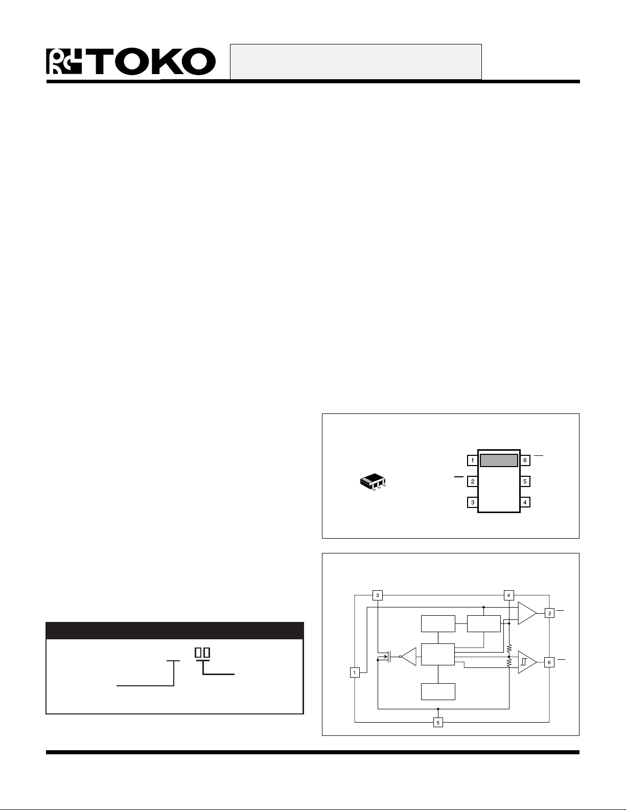
The TK652xx low power step-up DC-DC converter is
designed for portable battery powered systems, capable
of operating from a single battery cell down to 0.9 V. The
TK652xx provides the power switch and the control circuit
for a boost converter. The converter takes a DC input and
boosts it up to a regulated 1.8, 2.1, or 2.4 V.
The output voltage is laser-trimmed. Two internal detectors
monitor the output voltage and battery voltage. The Low
Output Indicator (LOI) generates an active low when the
battery voltage falls below 90 % of the output voltage. The
Low Battery Indicator (LBI) generates an active low when
the battery voltage falls below 1.1 V. These outputs can be
used to notify the microprocessor or power monitor circuit
of a fault condition. An internal Undervoltage Lockout
(UVLO) circuit is utilized to prevent the inductor switch
from remaining in the “on” mode when the battery voltage
is too low to permit normal operation. Pulse Burst
Modulation (PBM) is used to regulate the voltage at the
V
pin of the IC. PBM is the process in which an
OUT
oscillator signal is gated or not gated to the switch drive
each period. The decision is made just before the start of
each cycle and is based on comparing the output voltage
to an internally-generated bandgap reference. The decision
APPLICATIONS
■ Battery Powered Systems
■ Cellular Telephones
■ Pagers
■ Personal Communications Equipment
■ Portable Instrumentation
■ Portable Consumer Equipment
■ Radio Control Systems
is latched, so the duty ratio is not modulated within a cycle.
The average duty ratio is effectively modulated by the
“bursting” and skipping of pulses which can be seen at the
SW pin of the IC. Special care has been taken to achieve
high reliability through the use of Oxide, double Nitride
passivation. The TK652xx is available in a miniature
SOT-23L-6 surface mount package.
Customized levels of accuracy in oscillator frequency and
output voltage are available.
TK652xx
V
IN
LBI
SW
BLOCK DIAGRAM
LOI
GND
V
OUT
ORDERING INFORMATION
Voltage Code
VOLTAGE CODE
18 = 1.8 V
21 = 2.1 V
24 = 2.4 V
January 1999 TOKO, Inc. Page 1
TK652xxM
Tape/Reel Code
TAPE/REEL CODE
TL: Tape Left
TK652xx
ADVANCED INFORMATION
ABSOLUTE MAXIMUM RATINGS
All Pins Except SW and GND .................................... 6 V
SW Pin ....................................................................... 9 V
Power Dissipation (Note 1) ................................ 400 mW
Storage Temperature Range ................... -55 to +150 °C
Operating Temperature Range ...................-20 to +80 °C
Junction Temperature ...........................................150 °C
TK652xx ELECTRICAL CHARACTERISTICS
Over operating temperature range and supply voltage range, unless otherwise specified.
LOBMYSRETEMARAPSNOITIDNOCTSETNIMPYTXAMSTINU
V
NI
f
CSO
V
∆V
∆V
D
V
Note 1: Derate at 0.8 mW/oC for operation above TA = 25 oC ambient temperature, when heat conducting copper foil path is maximized on the printed
)GER(TUO
)DAOL(TUO
)ENIL(TUO
CSO
IBL
circuit board. When this is not possible, a derating factor of 1.6 mW/ °C must be used.
egatloVylppuS09.006.1V
ycneuqerFrotallicsOlanretnIT
VfodlohserhTnoitalugeR
TUO
VfonoitalugeRdaoL
VfonoitalugeReniL
)GER(TUO
)GER(TUO
A
T
A
V
NI
∆V
rotallicsOfooitaRytuDemit-nOT
A
dlohserhTrotacidnIyrettaBwoLT
A
C°52=273869zHk
C°52=%3-V
,V3.1=I
TUO
NI
I,V07.0=
TUO
Am4ot0=005Vm
Am1=
02-002Vm
TUO
%3+V
C°52=448445%
I,C°52=
TUO
Am1=50.101.151.1V
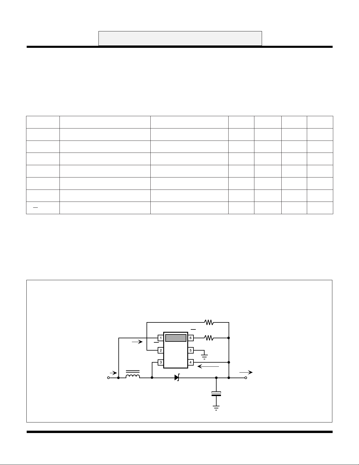
GENERAL CIRCUIT
V
LOI
300 kΩ
300 kΩ
OUTSW
I
I(V
)
OUT
OUT
V
OUT
C
V
IN
I(VIN)
I
B
V
IN
L
LBI GND
D
Page 2 January 1999 TOKO, Inc.
ADVANCED INFORMATION
FINAL TEST CIRCUIT
TK652xx
300 kΩ
LOI
300 kΩ
GND
V
OUTSW
R
OF
15
++
C
U
10 µF
C
10 µF
I
OUT
V
OUT
D
C
N
10 µF
I
B
V
IN
L = 95 µF
Note: Inductor L: Toko A682AE-014 or equivalent
Diode D: LL101
Capacitors CN:CD:CU: Panasonic TE series,
ECS-TOJY106R
V
IN
LBI
C
S
220 pF
R
1 K
D
S
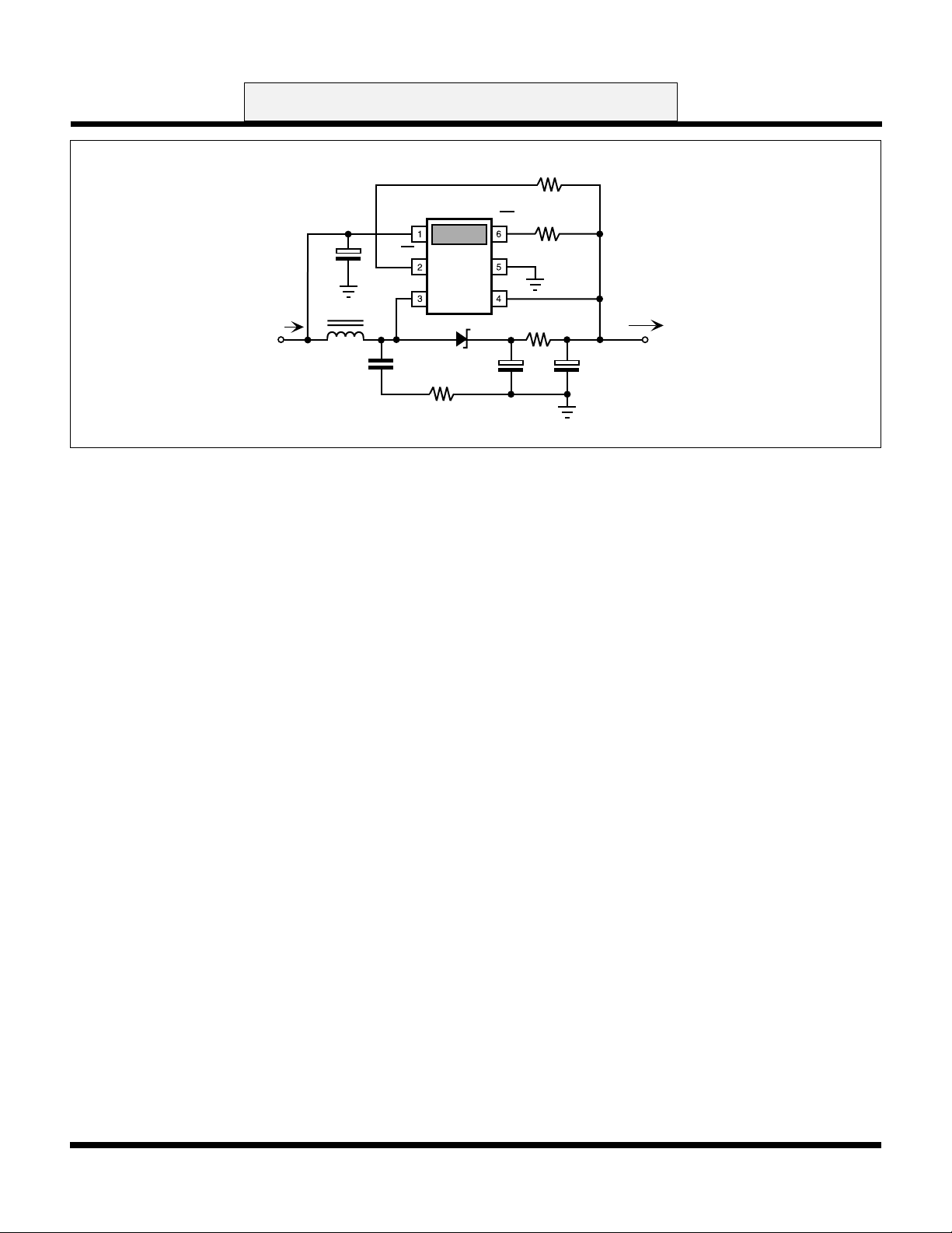
Above is the Final Test Circuit through which each of the production parts must pass. In this test circuit, the part is tested
against the specification limits in the data sheet (the min. and max. values in the Electrical Characteristics) at room
temperature, and is rejected if the tested values are outside the minimum (min.) and maximum (max.) values.
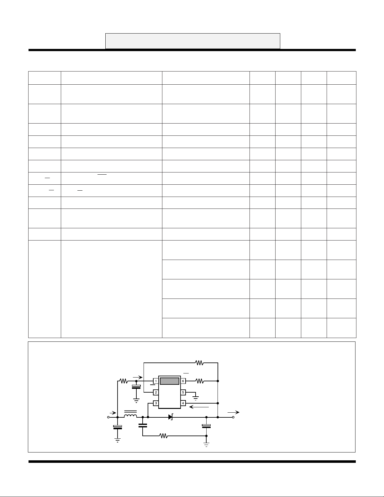
The Bench Test Circuits shown on the following pages are the circuits used most of the time to measure the typical (typ.)
values in the Electrical Characteristics section, and make the Typical Performance graphs.
Note: In measuring the oscillator frequency and the Max I
skipping” mode was achieved.
on the bench, the converter was loaded until “no pulse
OUT
January 1999 TOKO, Inc. Page 3
TK652xx
ADVANCED INFORMATION
TK65218 ELECTRICAL CHARACTERISTICS
Over operating temperature range and supply voltage range, unless otherwise specified.
LOBMYSRETEMARAPSNOITIDNOCTSETNIMPYTXAMSTINU
I
)Q(B
V(INI)VotnitnerruCtnecseiuQ
V(I
)VotnitnerruCtnecseiuQ
TUO
∆f
/∆T
CSO
V
∆V
V
∆V
R
TUO
)GER(TUO
/∆T
)IOL(TUO
)IOL(TUO
)NO(WS
FFE)3,2setoN(ycneiciffEretrevnoC
V
VLU
V
NI
)3etoN(tnerruCyrettaBdaoLoN
T
A
V
niP
NI
niPVNI,V3.1=I
TUO
VfodlohserhTnoitalugeR
TUO
VfoytilibatSerutarepmeT
V
TUO
V
)IOL(TUO
noitisnarTIOLgniruDV
siseretsyHdlohserhTT
niPWSfoecnatsiser-nOV
egatloVtuokcoLegatlovrednUT
NI
T
A
rotallicsOfoytilibatSerutarepmeTV
NI
T
A
V
)GER(TUO
NI
NI
A
TUO
V
NI
A
V
NI
V
NI
,V3.1=I
TUO
C°52=
,V3.1=I
TUO
C°52=
TUO
,V3.1=
,Am0=
,Am4ot0=
0406Aµ
1102Aµ
Am0=2102Aµ
gnippikSesluPoN
1.0C°/%
C°52=647.1008.1548.1V
,V3.1=I
TUO
T,V3.1=
A
Am1=001C°/mpp
C°52=55.126.186.1V
C°52=52Vm
V=
,T
)GER(TUO
A
I,V3.1=
TUO
C°52=0.1mho
,Am6=
lioC37D,Hµ001=L
67%
)4etoN(,C°52=74.097.0V
T,V9.0=
A
T,V1.1=
A
,C°52=
lioCFD3,Hµ59=L
,C°52=
lioCFD3,Hµ59=L
50.7Am
60.31Am
ImumixaM
I
)XAM(TUO
TUO
)3,1setoN(
Inductor L: Toko A682AE-014 or equivalent
Diode D: LL103A or equivalent
Capacitors CN:CO:CB: Panasonic TE series,
ECS-TOJY106R
V
R
N
1 K
I
B
IN
I(VIN)
C
N
10 µF
L = 95 µH
C
B
10 µF
retrevnoCrof
V
NI
T,V3.1=
A
lioCFD3,Hµ59=L
V
NI
T,V9.0=
A
lioC37D,Hµ93=L
V
NI
T,V1.1=
A
lioC37D,Hµ93=L
BENCH TEST CIRCUIT
300 kΩ
V
IN
LBI GND
C
S
220 pF
R
S
1 K
LOI
300 kΩ
V
OUTIND
I(V
)
OUT
D
C
10 µF
O
I
OUT
,C°52=
,C°52=
,C°52=
70.51Am
0.71Am
0.82Am
Note 1: Maximum load current depends on
inductor value and input voltages.
Note 2: Output ripple depends on filter
capacitor values, ESRs and the
inductor value.
Note 3: When using specified Toko inductor
and Schottky diode with VF = 0.45 V
@ 100 mA.
Note 4: Regulation not guaranteed.
V
OUT
Page 4 January 1999 TOKO, Inc.
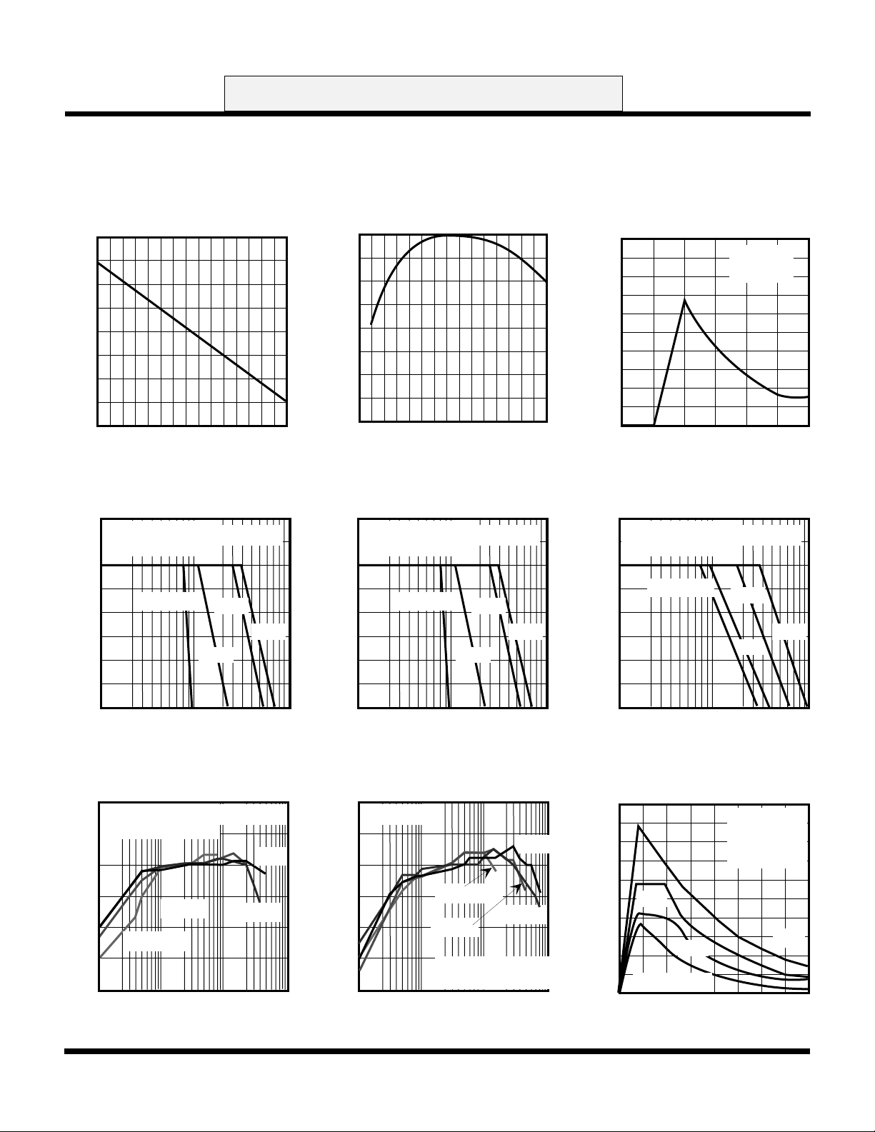
TK65218
V
(V)
V
(V)
V
(V)
ADVANCED INFORMATION
TYPICAL PERFORMANCE CHARACTERISTICS
TK652xx
OSCILLATOR FREQUENCY
TEMPERATURE
91
87
(kHz)
83
OSC
f
79
75
-50 0 50 100
TEMPERATURE (°C)
OUTPUT VOLTAGE
LOAD CURRENT
1.9
L = 95 µH
TOKO P/N: A682AE-014
(3DF SERIES)
TA = 25 °C
1.8
V
1.7
IN
= 0.9 V
1.3 V
OUT
1.6
1.1 V
VS.
VS.
1.6 V
OUTPUT REGULATION VOLTAGE
TEMPERATURE
1.800
1.795
(V)
1.790
OUT(REG)
V
1.785
1.780
-50 0 50 100
TEMPERATURE (°C)
OUTPUT VOLTAGE
LOAD CURRENT
1.9
L = 100 µH
TOKO P/N: 636CY-101M
(D73F SERIES)
TA = 25 °C
1.8
V
1.7
IN
= 0.9 V
1.3 V
OUT
1.6
1.1 V
VS.
1.6 V
VS.
BATTERY CURRENT
INPUT VOLTAGE
200
TA = 25 °C
160
NO LOAD
120
(µA)
B
I
80
40
0
0.1 0.5 1.0 1.5
VIN (V)
OUTPUT VOLTAGE
LOAD CURRENT
1.9
L = 39 µH
TOKO P/N: 636CY-390M
(D73 SERIES)
TA = 25 °C
1.8
V
= 0.9 V
IN
1.3 V
1.7
OUT
1.1 V
1.6
VS.
VS.
1.6 V
1.5
1 10 100
I
(mA)
OUT
EFFICIENCY VS. LOAD CURRENT
80
L = 95 µF
TOKO P/N: A682AE-014
(3DF SERIES) SMALL COIL
75
TA = 25 °C
70
65
EFF (%)
1.1 V
60
VIN = 0.9 V
55
50
0.1 1 10 100
I
(mA)
OUT
1.6 V
1.3 V
1.5
1 10 100
I
(mA)
OUT
EFFICIENCY
85
TA = 25 °C
VS.
LOAD CURRENT
80
75
70
VIN = 0.9 V
EFF (%)
65
60
55
1.1 V
L = 100 µF
TOKO P/N: A636CY-101M
(D73 SERIES) LARGER COIL
0.1 1 10 100
I
(mA)
OUT
1.6 V
1.3 V
1.5
1 10 100
I
(mA)
OUT
MAXIMUM OUTPUT CURRENT
INDUCTOR VALUE
100
NO PULSE
SKIPPING
MODE
TA = 25 °C
(mA)
80
60
1.3
40
OUT(MAX)
I
20
0
1.1 V
VIN = 0.9 V
0 40 80 120 160
INDUCTOR VALUE (µH)
VS.
1.6 V
January 1999 TOKO, Inc. Page 5
TK652xx
ADVANCED INFORMATION
TK65221 ELECTRICAL CHARACTERISTICS
Over operating temperature range and supply voltage range, unless otherwise specified.
LOBMYSRETEMARAPSNOITIDNOCTSETNIMPYTXAMSTINU
I
)Q(B
V(INI)VotnitnerruCtnecseiuQ
V(I
)VotnitnerruCtnecseiuQ
TUO
∆f
/∆T
CSO
V
∆V
V
∆V
R
TUO
)GER(TUO
/∆T
)IOL(TUO
)IOL(TUO
)NO(WS
FFE)3,2setoN(ycneiciffEretrevnoC
V
VLU
V
NI
)3etoN(tnerruCyrettaBdaoLoN
T
A
V
niP
NI
niPVNI,V3.1=I
TUO
VfodlohserhTnoitalugeR
TUO
VfoytilibatSerutarepmeT
V
TUO
V
)IOL(TUO
noitisnarTIOLgniruDV
siseretsyHdlohserhTT
niPWSfoecnatsiser-nOV
egatloVtuokcoLegatlovrednUT
NI
T
A
rotallicsOfoytilibatSerutarepmeTV
NI
T
A
V
)GER(TUO
NI
NI
A
TUO
V
NI
A
V
NI
V
NI
,V3.1=I
TUO
C°52=
,V3.1=I
TUO
C°52=
TUO
,V3.1=
,Am0=
,Am4ot0=
5456Aµ
5.2102Aµ
Am0=5.4132Aµ
gnippikSesluPoN
1.0C°/%
C°52=830.2001.2361.2V
,V3.1=I
TUO
T,V3.1=
A
Am1=001C°/mpp
C°52=38.198.159.1V
C°52=83Vm
V=
,T
)GER(TUO
A
,V3.1=I
TUO
C°52=0.1mho
,Am6=
lioC37D,Hµ001=L
87%
)4etoN(,C°52=84.097.0V
T,V9.0=
A
T,V1.1=
A
,C°52=
lioCFD3,Hµ59=L
,C°52=
lioCFD3,Hµ59=L
40.6Am
50.11Am
ImumixaM
I
)XAM(TUO
TUO
)3,1setoN(
Inductor L: Toko A682AE-014 or equivalent
Diode D: LL103A or equivalent
Capacitors CN:CO:CB: Panasonic TE series,
ECS-TOJY106R
I
B
V
IN
R
N
1 K
C
10 µF
L = 95 µH
C
10 µF
retrevnoCrof
V
NI
V
NI
V
NI
T,V3.1=
A
T,V9.0=
A
T,V1.1=
A
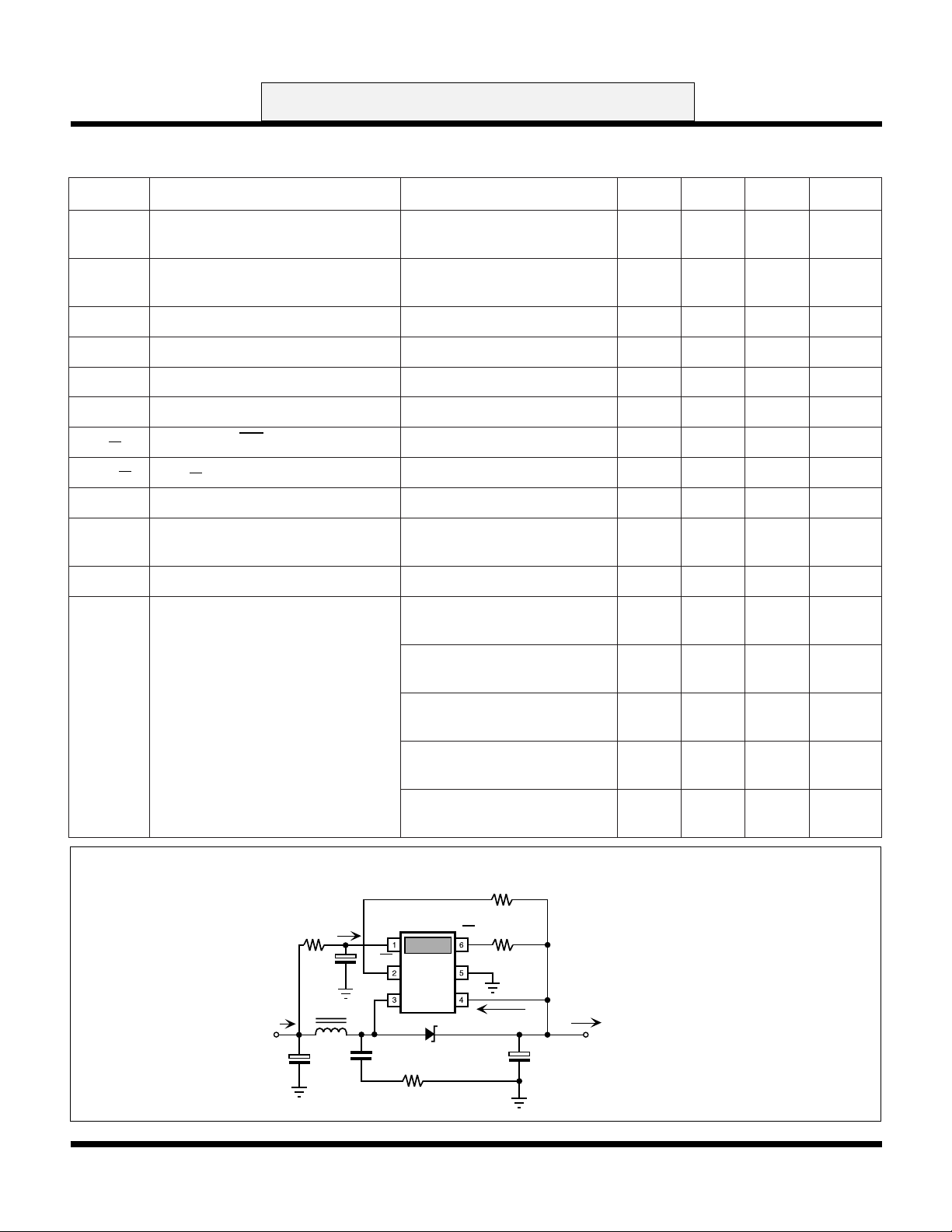
BENCH TEST CIRCUIT
300 kΩ
LOI
300 kΩ
V
OUTIND
I(V
OUT
B
N
I(VIN)
V
IN
LBI GND
C
220 pF
D
S
R
S
1 K
,C°52=
lioCFD3,Hµ59=L
,C°52=
lioC37D,Hµ93=L
,C°52=
lioC37D,Hµ93=L
60.31Am
0.51Am
0.42Am
Note 1: Maximum load current depends on
inductor value and input voltages.
Note 2: Output ripple depends on filter
capacitor values, ESRs and the
inductor value.
Note 3: When using specified Toko inductor
and Schottky diode with VF = 0.45 V
@ 100 mA.
Note 4: Regulation not guaranteed.
I
C
10 µF
OUT
V
OUT
O
)
Page 6 January 1999 TOKO, Inc.
 Loading...